© 2016, IRJET | Impact Factor value: 4.45 | ISO 9001:2008 Certified Journal | Page 1169
Processor Design: An Optimization Approach
Jiger Prakashchandra Acharya
Lecturer(Computer Department),Government Polytechnic-Ahmedabad,Gujarat,India
---***---Abstract -
Processor design is an interesting research areain hardware and electronics field. Processors can be classified as general purpose and/or specific application oriented to design them is a complex task as many components are required to integrate. To minimize the size, cost, weight and power requirement are big challenging issues to handle and at the same time obtained the performance is a great task to achieve. Optimization is a best approach to deal with such issues.
Key Words: Processor, memory, input output, clock,
cycle, hardware design components
1.INTRODUCTION
Processor is a unit which take input from input device process it and generate the output. Processing logic can be of many types depending on the application or the user requirements. General purpose processor has generic logic while application oriented or specific processor have their own logic. The variety of inputs mechanism may be via keyboard, mouse, and controller sensors or via user interface. Output may be in form of commands, signals, to drivers which control the automated or generic process. Memory is an very important part which require to store the processor’s logic or input and/or output data. Processor has no natural sense like human so it’s responsibility of it’s manufacturer or designer to put artificial intelligence in it. Such intelligence can be achieved through developing logic in processor.
Fig -1: Block diagram of Generic Processor
Processor performs various actions depending on such logic and process input data that data may be come from number of ways like direct data feeding through input devices or indirect data feeding which include data from sensors, command signals or in some different form of analog and/or digital signals like pressure, temperature, current, voltage level humidity, voice,image or video signal. Through transducer any non electrical signals can be converted into electrical analog signal and through Analog to Digital signal we have all the input data now in the form of digital signals which can represented by various combination of zero(0) and Ones(1) so we have to deal with 0 and/or 1 only. Various logic can be
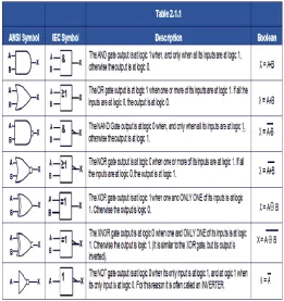
[image:1.595.309.571.249.527.2]achieved through use of single and/or multiple logic gates. Available logical gates are as under
Table -1: Functionality of various Gates
(ref: http://www.learnaboutelectronics.org//Digital/dig21.php)
Typical processor has to optimum use of its all resources which are
1) Bus System 2) Memory unit 3) input /output system 4) Instruction set
2. BUS SYSTEM
© 2016, IRJET | Impact Factor value: 4.45 | ISO 9001:2008 Certified Journal | Page 1170
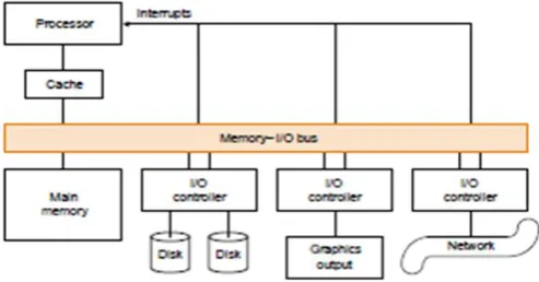
take i/p data for processing and generate the output data. ThePerformance of the processor also depends on the Bus performance. We can also utilize it as common memory bus and/or input/output Bus as shown in figure below.
Fig -2: Interonnection of processor and I/O
2.1Types of Buse
1) processor-memory (short high speed, custom design) is highly desirable
2) backplane must be high speed and standardized so technical advancement, e.g., PCI)
3) I/O (lengthy, different devices, standardized, e.g., SCSI)
Shared communication link (one or more wires)
Difficult to design and has to resolve the following issues:
1) Bus design may be bottleneck for the i/o bound jobs 2) length of the bus may affect the data transfer rate 3) number of devices is also a limiting factor for the communicating with i/o devices so tradeoffs (buffers for higher bandwidth vs. latency) must be done for efficient use 4) support for many different devices are desirable as user can attach any devices
5) cost is always a big factor for the end user.
3. Input /Output SYSTEM
may be affected by following aspects:
1)Access latency is the requirement of time to take any data from memory or i/o devices to processor environment. 2) Throughput which related with the amount of output to given input.
3) Connection of Devices also matter to transfer the data to/from processor to/from i/o or memory.
[image:2.595.312.558.123.266.2]4) Hierarchy of memory also play a major role in the performance of Processor which may be various types of ROMs(Read Only Memories)where no change of data or memory is possible so it also called Hard-wired programming but in PROM(Programmable Read Only Memory) user can alter the content of memory by small programming in EPROM(Erasable Programmable Read Only Memory) where user can have its user space which can be write and/or erase , EEPROM(Electrically Erasable Programmable Read Only Memory) where through electrically erase the PROM.
Table -1: Typical data transfer rate of various I/O and memory devices
There are 3 main mode of data transfer
1) Programmed I/O in which processor check input device buffer for read and output device buffer for write purpose. 2) Interrupt Mode: Processor wait devices to advertise its “Ready” state for read/write purpose either by interrupt signal or by status register.
3)Direct Memory Access(DMA): in which Processor release the control of bus system and DMA controller take charge of bus system and perform data transfer from memory to/from i/o devices directly.
3.1 Polling and Interrupt – driven I/O
In polling processor has to continuously check the status of various input devices for their meaningful new information. Processor has to look up all the times for peripherals response, while in interrupt driven I/O device will inform the processor for the data send/receive process. Various types of interrupts Hardware, software, and programming with exception can be developed. Interrupts can be developed
1) External Interrupts: generated by peripherals i/o devices which are random in nature and not related with programming logic
2) Internal Interrupts generated by Processor when some type of hardware or software error is generated they are related with program execution.
3) Program Interrupt: initiated by external or internal signals in nature in which starting address of ISR (Interrupt Service Routine) is specified by the interrupting hardware devices. Interrupt procedure or cycle generally stores all necessary information to restore the state of Processor after completion of the service routine.
4. Memory Hierarchy
[image:2.595.39.286.155.284.2]© 2016, IRJET | Impact Factor value: 4.45 | ISO 9001:2008 Certified Journal | Page 1171
greatly depend on the Memory backbone so provide adequatestorage with processor is essential this can be done by following ways:
1) Use various types of memories depend on their cost/performance or cost benefit ratio.
2) Automatic space allocation methods in Memory paradigm. 3) Develop virtual memory concept.
4) Design of communication links
Mainly there are two types of task associated with processor 1) Processor bound which require the support of processor to accomplish such task
2) I/o bound which require the main support of input /output peripherals.
4. 1 Characteristic of Memory
1)Location: is the place where the memory component established depending this it is known as internal memory which may be Inside CPU or outside CPU) or external memory which is outside CPU.
2)Hierarchy: based on that Primary memory or secondary memory .Primary memory consist of typesof RAM and ROM while secondary memories include hard disk and also external memories.
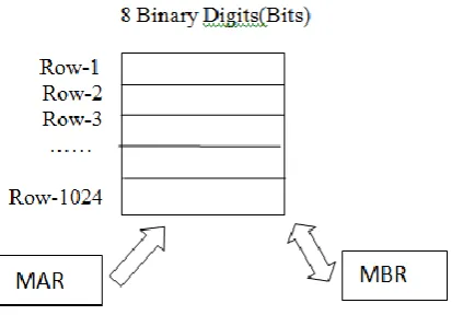
3)Capacity: depending on the how much data it can be stored transfer in byte(8 bits),word(16 bits)or block of data. As shown in figure 1K X 8 memory unit it mean that each line or row of memory contain 8 bits or 1Byte and such 1024 lines are available with memory system.
Fig -3: 1K X *8 memory module with Address and Data register
4. 2 Access types of Memory
Memories also categories depending on how we access them in sequence called sequential access out of sequence called random access. Memory access also related with how we address it which related with addressing modes which are as follows:
1) Immediate Addressing: the interested data is just available with next location to processor called immediate addressing mode.
2) Direct Addressing: the address of interested data is available with Processor called direct addressing mode. 3) Indirect Addressing: the address of interested data address is available with Processor called in-direct addressing mode. 4) Register Addressing: the interested data is stored in internal registers of processor called Register Addressing mode. 5) Index Addressing: the data is stored in the Source Index (SI) and/or Destination Index(DI) it called Index Addressing mode.
6)Implied Addressing: the interested data is available with processor environment and no any external address is required to supplied as data is on-hand with processor.
7) Base Addressing: the interested data can be obtained by the adding the offset address with the base address which is called its physical or actual address.
Base on construction: memory can be classified as optical, magnetic or semi-conductor types of memories.
In Magnetic tap type of memory data bits are stored in magnetized manner on the tape.Magnetic head reader is there to access the data which are there on particular sector, track,or cylinder.magnetic material is widely used in storage media. 2)Optical media: bits are stored on optical media and optical reader is required to read and/or write them.
Fig -4: Graphical view of Hard Disk
Fig -5: Logical View of sector,track on cylinder
[image:3.595.68.280.481.625.2] [image:3.595.309.575.584.694.2]© 2016, IRJET | Impact Factor value: 4.45 | ISO 9001:2008 Certified Journal | Page 1172
To identify the particular data from its sector is called Seektime
Fig -6: Comparision of varioustypes of memories
5. Instruction set
Each processor is required the support of instruction to perform any task. The task which should be performed is stored in instruction in form of bits. Generally Instruction has two parts opcode and operands.OPCODE is the operation code which relate with the which type of task required to perform and OPREANDS is the data on which the operation is required to execute. Instructions can be further classified according to task perform by them
1)Data transfer instruction mainly deal with the transfer of data to/from processor.
2)Arithmatic Instructions mainly perform various arithmetic operations on the data
3)Logical Instruction perform the logical operation on the data bit by bit
4)Shift and rotate instructions: mainly perform shift left ,right and various rotate instructions.
5)Branching instruction :when some condition is required to be checked on some parameters and then further processing is required to be executed at that point branching instructions required.
6)Processor initiated and special instruction: some instructions required to execute for the processor check points such special instructions are not process any data but used to regulate the normal functionality of processor.
Further any instruction of any above mentioned category should have following characteristic:
1) Complete: it must be used for variety of applications
2) Efficient: it must be efficient in terms of memory requirements and hardware realization and generate the optimum code.
3)Regular: expected instruction must be exist and supported by processor.
4)Compatible: Programs written for one processor can be
used on the next or similar versions of it.
5) Instruction set should be SIMPLE easy to implement and SMALLER only essential instructions are required so easy of learning and understanding can be developed.
6) Instruction set must be PRIMITIVE it must support all the basic functionalities.
7) Consistence: Instruction set must be applicable to general rules uniformly.
8) Orthogonality: Instruction set must posses independent non-interfering features.
9) Transparent: Instruction set must not have any visible side effect due to implementation details.
10) Extensibility: Instruction set must be extensible in nature to allow the additional future capabilities.
Each instruction is required to fetch from the input devices then decode by the processor logic and then execution of such instruction can be performed.
Instructions are also categorized depend on the no of operands requirements or based on the size of instruction
1) 1-Byte or Single byte instructions which required only OPCODE
2) 2-Bytes instructions in which 1 Byte for OPCODE and 1Byte for OPREAND
3) 3-Bytes instructions in which 1 Byte for OPCODE and 2 Bytes for OPREAND
6. CONCLUSIONS
Performance of any processor is determined by the its
[image:4.595.37.253.127.290.2]© 2016, IRJET | Impact Factor value: 4.45 | ISO 9001:2008 Certified Journal | Page 1173
that optimization has crucial role to finalize the aboveparameters.
ACKNOWLEDGEMENT
Author heartly thankful and oblige Dr. Arun K.Somani for their informative guidance given in the Short term training held at L.D.College of Engineering Computer Department which enlighten to write such article in this domain.
REFERENCES
[1] Samiappa Sakthikumaran,S.Salivahanan and V.S.Kaanchana Bhaaskaran , June 2011, “16-Bit RISC Processor Design For Convolution Application”,IEEE International Conference on Recent Trends In Information Technology, pp.394-397.
[2] Rohit Sharma, Vivek Kumar Sehgal, Nitin Nitin1, Pranav Bhasker, Ishita Verma , 2009, “Design And Implementation Of 64-Bit RISC Processor Using VHDL”,UKSim : 11th International Conference on Computer Modeling And Simulation, pp. 568 – 573.
[3] Rupali S. Balpande and Rashmi S. Keote.2011, “Design of FPGA based Instruction Fetch & Decode Module of 32-bit RISC (MIPS) Processor, International Conference on Communication Systems and Network Technologies pp. 409 – 413
[4] Sivarama P.Dandamudi ,”A Guide To RISC Processor For Programmers And Engineers”, Springer. [5] Tom Wada, “Small Risc Processor (SPR) design specification v1.0”, 12th Design Contest In OKINAWA, pp. 1-17
[5] Dr.Arun.K.Somani, Anson Marston Distinguished Professor,Department of Electrical and Computer
Engineering,Iowa State University,Ames, IA 50011 course materials on “Fundamental tradeoffs in Computer Design and Organization” GIAN STTP at L.D.College of Enggineing.
BIOGRAPHIES
Jiger Prakashchandra Acharya is

![Crystal structure of 1 [(1 methyl 5 nitro 1H imidazol 2 yl)methyl]pyridinium iodide](data:image/gif;base64,R0lGODlhAQABAIAAAP///wAAACH5BAEAAAAALAAAAAABAAEAAAICRAEAOw==)