International Journal of Emerging Technology and Advanced Engineering
Website: www.ijetae.com (ISSN 2250-2459, ISO 9001:2008 Certified Journal, Volume 5, Issue 3, March 2015)
172
Electrical and Micro-structural Properties of Cadmium
Chalcogenides: A Comparative Study
V. K. Kamble
1, V. B. Pujari
2 1,2Materials Research Laboratory, Dept. of Physics, KBP College, Vashi, Navi Mumbai, M.S, India.
Abstract— By considering the practical importance of Cadmium chalcogenide, CdX (X = S, Se, Te), thin films of these materials were deposited onto the glass micro slides by a chemical bath deposition technique. These as deposited samples were thin, uniform, adherent and diffusely reflecting. These thin films were characterized to understand the electrical conduction mechanism involved in these films at ambient and higher temperatures. The thermo-electric power measurements were also made to know the type of conduction mechanisms involved therein. The possible conduction mechanism has been discussed which indicate that the electric transport properties of cadmium chalcogenides is mainly governed by the intergrain barrier potential scattering. These as-deposited thin film samples were further characterized and analyzed by low angle X-ray diffraction technique and scanning electron microscopy for their structures and surface morphological information respectively, which reveals the polycrystalline nature of these cadmium chalcogenide thin films.
Keywords— CdX (S, Se, Te), structural, microscopic and electrical properties.
I. INTRODUCTION
Thin chalcogen films of II-VI, IV-VI, and II-IV-VI families have already been emerged as the potential candidates of high performance and low production cost. High absorption coefficients and nearly matching band gaps are the root causes of their popularity. Cadmium chalcogenides, CdX (X= S, Se, Te) occupy a challenging place among nanoscale semiconductors of the different chemical nature due to popularity in both experimental studies and applications [1-2]. The synthesis of binary metal chalcogenides of group II-VI semiconductors in a nanoparticle form has been a rapidly growing area of research due to their important non-linear optical properties, luminescent properties, quantum-size effect etc [3-4]. They have been proved their ability as the efficient absorbers and their applications in thin film photovoltaic and optoelectronic devices in general [5-6]. In particular, Cadmium sulphide has many applications such as field effect transistors, light emitting diodes; photo catalysis and window layer [7-8]. Cadmium selenide has applications in solar cells, photo-electrochemical cells, gamma-ray detectors and thin film transistors etc [9].
Furthermore, Cadmium telluride is a strong contender for useful for a large scale thin film devices technology such as in solar cells, IR and gamma-ray detectors, field effect transistors, switching devices and Schottky barriers etc [10-11]. In recent years, there has been growing interest in developing techniques for preparing semiconductor nanoparticles and thin films because the properties in nano form differ significantly from those of their bulk counter parts [12]. Therefore, efforts are made to study the electrical transport properties viz. electrical conductivity at ambient and higher temperatures and thermo-electric power measurements and their structure, crystallinity and surface morphology of these cadmium chalcogenide thin films.
II. EXPERIMENTAL DETAILS
Cadmium chalcogenide, CdX (X = S, Se, Te) thin films were deposited onto glass micro slides by chemical bath deposition technique. For deposition of these films, equimolar solutions of appropriate precursors (AR grade) were taken in a stoichiometric proportion. Triethanolamine was used as a complexing agent and pH of the reaction mixture was adjusted to 10.5 by adding the adequate quantity of sodium hydroxide. Glass micro slides / substrates were then mounted vertically on a specially designed substrate holder and kept rotated at constant speed, which offers a continuous and uniform mechanical churning of the reaction mixture. To obtain quality samples, deposition temperature, time for deposition and speed of substrate rotation were optimized and were found to be 60oC, 90 min. and 70 2 rpm respectively. The film compositions were then analyzed and computed by an EDS technique.
International Journal of Emerging Technology and Advanced Engineering
Website: www.ijetae.com (ISSN 2250-2459, ISO 9001:2008 Certified Journal, Volume 5, Issue 3, March 2015)
173
The thermo-emfs were measured with a HP- 6½ digit multimeter. The temperature gradient was recorded with an Agronic 113, 4½ digit dc micro-voltmeter. Silver paint was applied at the ends of these films for ohmic contact purpose.
The X-ray diffractograms were obtained for these films to get the structural / crystallographic information pertaining to interplaner distance and lattice parameters etc. Philips PW-3710 X-ray diffractometer was used for this purpose. The range of the scanning angles (2) was varied from 20 to 80o. Further, the surface morphology of these samples was observed through a scanning electron microscope (SEM), Cameca SU-30 (France).
III. RESULTS AND DISCUSSION
Cadmium chalcogenide thin films were deposited by Chemical Bath Deposition Technique, which is a simple, scalable and convenient for large area deposition. The as-deposited films were thin, uniform, mechanically hard and diffusely reflecting in nature. Thickness of these films was determined with an interference technique discussed elsewhere. The compositional analysis of these samples was carried out with the help of EDS technique.
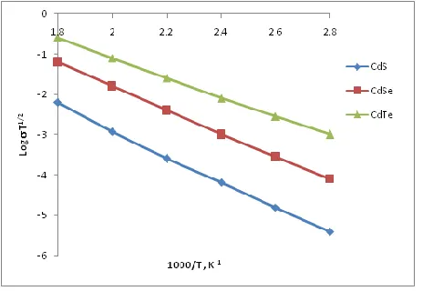
The ambient temperature dc electrical conductivities of these as-deposited cadmium chalcogenide thin film structures were measured in 300-600 K temperature range and their temperature dependence can be fitted to the Arrhenius relation as,
[image:2.612.329.561.112.283.2] = 0 Exp (- Ea/ KT ) … (1) Where Ea is the activation energy of an electrical conduction process and the other terms have their usual meanings. The plots of Log versus inverse of absolute temperature (Fig. 1) for these thin films were analyzed to determine the modes of conduction mechanism and the electron activation energies in both the high and low temperature regions. It has been seen that the conductivity has increased with increase in temperature. The electron activation energies in both high and low temperature regions were computed and cited in Table I.
Fig. 1 Variation in electrical conductivity with working temperature.
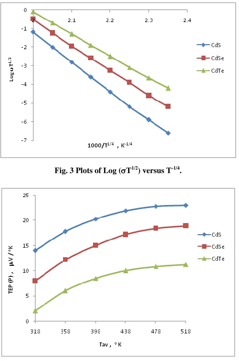
The variation in electrical conductivity with temperature showed two distinct conduction regions corresponding to two different conduction mechanisms and activation energies. The analysis of these conduction mechanisms in two different regions is therefore of much importance. Fig. 2 showed such an analysis wherein the high temperature region is characterized by a grain-boundary scattering limited conduction mechanism and Fig. 3 showed hopping conduction mechanism which is a characteristic of conduction in low temperature region [13-15].
[image:2.612.330.562.426.586.2]International Journal of Emerging Technology and Advanced Engineering
Website: www.ijetae.com (ISSN 2250-2459, ISO 9001:2008 Certified Journal, Volume 5, Issue 3, March 2015)
174
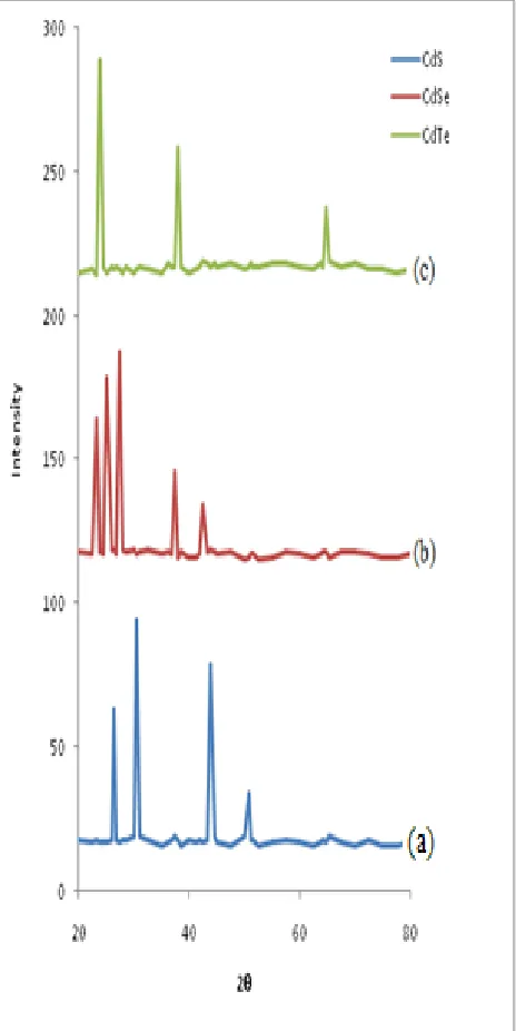
[image:3.612.50.289.210.570.2]The thermo-emf character of these chalcogenides was studied and analyzed by establishing the temperature gradient and measuring the resulting voltages across the ends of these thin film samples. The thermally generated voltage was measured in the temperature range 300-500 K and is as shown in Fig. 4.
Fig. 3 Plots of Log (T1/2) versus T-1/4.
Fig. 4 Temperature dependence of thermo-electric power.
The thermo-electric voltage generated was found to be negative for all these chalcogenides, indicating n-type conduction. It has been further observed that the variation in thermo-emf was approximately linear at low temperatures, but exhibit non-linear behavior at higher temperatures, obeying the power law dependence of temperature. This suggests that these materials are of non-degenerate type, and for such semiconductors, the thermo- electric power is weak. The thermo-electric power is expressed as,
P = - K /e [ (r + 5/2) + ln (2{2 m*d KT)3/2 / nh3})]… (2)
Where A = r + 5/2 is a thermo-electric factor that depends on various scattering mechanisms, m*d is the density of states effective mass, ‘n’ is the carrier density and other parameters have their usual meanings. The thermo-electric power (P) and the carrier concentration (n) are related as,
P = 200 (19.4 – log n) … (3)
The carrier mobility () were then determined by using a standard relation,
= / n e … (4)
The values of R.T. dc conductivity, carrier density and mobility for these chalcogenides are cited in Table II. It has been seen that the carrier density and mobility are the functions of the temperature. The variation in carrier mobility is significant as compared to the carrier density, which is suggestive of scattering mechanism is governed by the crystalline barrier potential [15]. The inter-crystalline barrier potentials (B) were therefore computed and cited in the Table I.
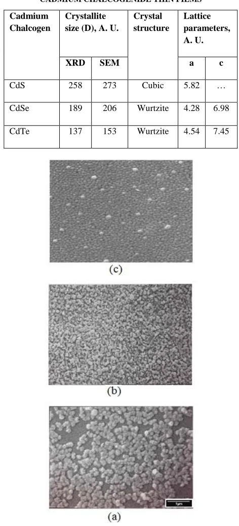
The X-ray diffractograms (XRD-patterns) of these thin films were obtained within the scanning angle (2) range 20 to 80o and are shown in Fig. 5.
These films were observed to be polycrystalline in nature. The pure cadmium sulphide (CdS) thin film exhibits cubic zinc-blend structure with spherical crystallites. The prominent peaks for CdS observed were (111), (200), (220) and (311) corresponding to (2) values of 26.3o, 30.5o, 43.9o and 50.8o respectively. The lattice parameter, ‘a’ was found to be 5.87 A.U. Furthermore, cadmium selenide (CdSe) and cadmium telluride (CdTe), both the thin films exhibit wurtzite structures. The lattice parameters, ‘a’ and ‘c’ for both CdSe and CdTe were calculated and are cited in Table 2. The prominent peaks for CdSe observed were (100), (002), (101), (110) and (202) corresponding to (2) values of 23.2o, 25.1o, 27.8o, 37.5o and 42.8o respectively and those for CdTe were (002), (110) and (211) corresponding to (2) values of 23.8o, 37.9o and 64.7o respectively. The observed prominent peaks, their intensities and lattice parameters for all these thin films were found in good agreement with their JCPD values. An average crystallite sizes (D’s) for all these thin films were also determined by Scherer’s relation,
International Journal of Emerging Technology and Advanced Engineering
Website: www.ijetae.com (ISSN 2250-2459, ISO 9001:2008 Certified Journal, Volume 5, Issue 3, March 2015)
175
[image:4.612.310.573.155.526.2]Where, k = 0.94 is a constant related to the shape of the crystallites, ‘’ is the wavelength of the incident radiation, ‘B’ is the full-width at half-maxima (FWHM) and ‘’ is the diffraction angle. The average crystallite sizes and lattice parameters are cited in Table III.
Fig. 5 XRD diffractograms of cadmium chalcogenides: (a) CdS, (b) CdSe and (c) CdTe.
TABLE I
ELECTRICAL TRANSPORT PROPERTIES OF CADMIUM CHALCOGENIDE THIN FILMS.
Cadmium Chalcogen
Electron
Activation Energy (Ea), eV.
Donar Levels (Ed), eV.
The inter-crystalline barrier potentials (B), eV.
HT LT
CdS 0.76 0.45 0.59 0.79
CdSe 0.67 0.28 0.46 0.63
CdTe 0.48 0.12 0.31 0.48
TABLE II
ELECTRICAL TRANSPORT PROPERTIES OF CADMIUM CHALCOGENIDE THIN FILMS (CONTD.)
Cadmium
Chalcogen
At Ambient Temperature (Room Temperature)
Electrical Conductivity,
, 10-5
(- cm)-1
Carrier Density,
n, 1019
cm-3
Carrier Mobility,
, 10-5,
cm2/ V.s
CdS 3.90 2.32 1.05
CdSe 7.36 3.82 1.20
CdTe 9.87 4.03 1.53
[image:4.612.53.285.204.667.2]International Journal of Emerging Technology and Advanced Engineering
Website: www.ijetae.com (ISSN 2250-2459, ISO 9001:2008 Certified Journal, Volume 5, Issue 3, March 2015)
[image:5.612.49.285.159.678.2]176 TABLE III
STRUCTURAL AND MORPHOLOGICAL PROPERTIES OF CADMIUM CHALCOGENIDE THIN FILMS
Cadmium Chalcogen
Crystallite size (D), A. U.
Crystal structure
Lattice parameters, A. U.
XRD SEM a c
CdS 258 273 Cubic 5.82 …
CdSe 189 206 Wurtzite 4.28 6.98
CdTe 137 153 Wurtzite 4.54 7.45
Fig. 6 SEM Micrographs of Cadmium chalcogenides: (a) CdS, (b) CdSe and (c) CdTe.
IV. CONCLUSION
These as-deposited films were thin, uniform, smooth, mechanically hard and diffusely reflecting. The dc electrical conductivity is increased because of the decrease in activation energy, donar levels, inter-crystallite barrier potential and crystallite size of these semiconductors. The thermo-electric power measurements revealed that these semiconductors exhibit n-type conduction. Cadmium sulphide thin film showed Zinc-blend structure. Cadmium selenide and telluride thin films showed wurtzite structures with their lattice parameters in good agreement with their JCPD values. Surface morphological studies revealed that the cadmium chalcogenide thin films were polycrystalline in nature. The crystallite sizes determined from the XRD and SEM studies were in good agreement.
Acknowledgment
The authors are thankful to the authorities of Rayat Shikshan Sanstha, Satara and Hon. Dr. V. S. Shivankar, principal, Karmaveer Bhaurao Patil College, Vashi, Navi Mumbai for their motivation and constant support to carry out the research activity.
REFERENCES
[1] Rogach, A. 2008. Semiconductor Nanocrystal Quantum Dots. (Ed.). Springer Wien New York.
[2] Delerue, C. and Lannoo, M. 2004. Nanostructures. Theory and Modeling. Springer-Verlag, Berlin, Heidelberg.
[3] Ghosh, S. A. Mukharjee, H. Kim. and Lie, C. Mater. Chem. Phys. 78 (2003), 726.
[4] Dwivedi, D. K. Dayashankar, M. and Dubey, J. Ovonic Res. 6 (2010), 57.
[5] Dhumure, S. S. and Lokhande, C. D. Ind. J. Pure & Appl. Phys. 31 (1993), 512.
[6] Hyeong, L. J. Thin Solid Films. 431 (2003), 344.
[7] Sarma, K. C. Bordolo, R. K. Sarma, M. and Ganguly, J. N. J. Instrum. Soc. India. 31 (2001), 216.
[8] Pujari, V. B. Int. J. Appl. Innov. Engg. Mgt. V2. I4 (2013), 339. [9] Lade, S. J. Uplane, M. D. and Lokhande, C. D. Mat. Chem. Phys. 68
(2001), 36.
[10] Ubale, A. U. and Kulkarni, D. K. Ind. J. Pure & Appl. Phys. 44 (2006), 254.
[11] Rusu, G. G. J. Optoelectron. and Adv. Mater. 3 (2001), 861. [12] Henglein, A. Chem. Rev. 89 (1989), 1861.
[13] Patil, V. B. Sutrave, D. S. Shahane G. S. and Deshmukh, L. P. Ind. J. Pure & Appl. Phys. 39 (2001), 184.
[14] Masumdar, E. U. Gaikwad, V. B. and Deshmukh, L. P. J. of Mater. Sci: Mater. Electron. 14 (2003), 43.
[15] Petritz, R. L. Phys. Rev. 104 (1956), 1508.