International Journal of Emerging Technology and Advanced Engineering
Website: www.ijetae.com (ISSN 2250-2459, ISO 9001:2008 Certified Journal, Volume 4, Issue 8, August 2014)
531
A PID Compensator Control for the Synchronous Rectifier
Buck DC-DC Converter
Nivya K Chandran
1, Mary P Varghese
21Student, 2Associate Professor, Dept of Electrical and Electronics Engineering,Vidya Academy of Science and Technology,
Thrissur
Abstract—This paper aims to design a PID compensator for the control of Synchronous Rectifier (SR) Buck Converter to improve its conversion efficiency under different load conditions. Since the diode rectifier is replaced by a high frequency MOSFET switch, the SR control method itself will be sufficient under heavy load condition, to attain better normal mode performance. However, this technique does not hold well in light load condition, due to increased switching losses. A new control technique accompanied with PID compensator is introduced in the paper will enable synchronous buck converter to realize ZVS, while feeding light loads. This is also least cost and highly efficient easy technique without use of extra auxiliary switches and RLC components. This control technique also proved to be efficient under input voltage variations. Simulation is done in MATLAB Simulink for proving stabilization provided by the PID compensator for synchronous rectifier (SR) buck converter.
Keywords—Synchronous Rectifier (SR), Continuous Condu-ction Mode (CCM), Discontinuous Conduction Mode (DCM), Zero Voltage Switching (ZVS), Proportional-Integral-Derivative (PID).
I. INTRODUCTION
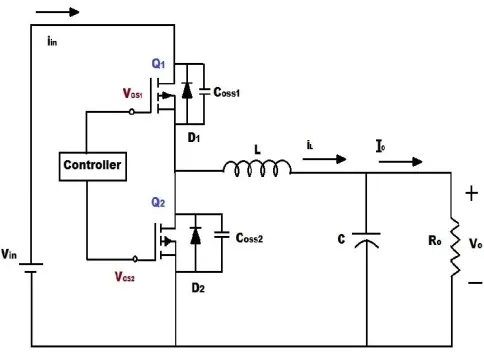
The synchronous buck DC-DC converter consists of two MOSFETs that are synchronized in operation. The auxiliary MOSFET is used in place of freewheeling diode so that conduction loss is reduced. Synchronous Buck converter [2] is similar to the conventional asynchronous buck converter except the freewheeling diode is paralleled with SR switch Q2. It is called a synchronous buck converter because the SR switch Q2 is synchronously turned on and off with the main switch Q1 operation and is shown in figure I. The primary idea of a synchronous buck converter [4] is to utilize a MOSFET as a rectifier that has very low forward voltage drop in comparison to a diode rectifier.
By lowering the forward voltage drop of diode, the overall efficiency for the conventional buck converter can be increased. Thus, the synchronous buck topology has improved efficiency and synchronous rectifier (SR) switch (MOSFET Q2) requires a PWM signal that is the complementary of the primary PWM signal.
[image:1.612.324.566.270.448.2]The SR switch Q2 is turned on when main switch Q1 is off and vice versa. This PWM format is called Complementary PWM.
Figure I. Synchronous Buck DC-DC Converter
The body diode of MOSFET Q2 acts as a slow rectifier and would add only allowable losses. Because the synchronous rectifier switches with lower than a volt across itself, the switching losses will be almost zero. The MOSFET conduction losses are very lesser in comparison to the forward voltage drop of schottky rectifier. Synchronous Rectification can increment portable device switching converter’s efficiency significantly with minimum cost [5]. During steady state situations, this cycle of switching main and auxiliary MOSFETs ON and OFF complementary to each other maintains VO to its desired value. So there is a need to reduce these switching losses using control techniques and to improve the light load efficiency.
International Journal of Emerging Technology and Advanced Engineering
Website: www.ijetae.com (ISSN 2250-2459, ISO 9001:2008 Certified Journal, Volume 4, Issue 8, August 2014)
532
According to the previous researches, the PWM-controlled converter has lower conversion efficiency than the PFM-controlled converter in light loads, whereas in heavy load condition, the PWM-controlled converter has got better conversion efficiency compared to PFM [11][14]. Therefore, some studies decided to combine the advantages of both the control methods to form a new control method called Dual mode control. PFM is used in light load condition, whereas PWM is chosen in heavy load condition. This method can achieve better efficiency and also the nonlinear inductor is used for lowering switching frequency at light load condition [25]. However, large output voltage transients and sub harmonic noise occurs during transition between PWM and PFM. The switching frequency is unpredictable and also requires complicated fabrication materials because of the variable frequency operation. But other technique namely resonant gate drive uses an inductor and two diodes provided to clamp and recover drive energy (clamped gate voltage). Also the circuit timing is adjusted to cycle inductor current during driving transitions (fast driving speed) [15]-[17]. But the requirement of extra auxiliary switch and passive components and gate-source voltage over drive are its disadvantages. Several techniques like zero voltage switching (ZVS) [18]-[20] and digital control [21][23], have been used, but the applications of these techniques are seem to be much complicated. ZVS and the digital control technique have better performance but need extra auxiliary switches and RLC passive components. Moreover, the controller used is a digital system processor which will result overall cost to be high.The new control strategy with PID compensator in this paper enables an SR buck converter to have increased light load efficiency with ZVS technique without the requirement of extra auxiliary switches or RLC passive components. This control method is of least cost and the technique is also easy. Moreover, the output voltage V (t) must be kept within specified limits irrespective of the changes in the input line voltages and output loads. This is accomplished by using negative- feedback control system, where converter output VO is compared with its reference value VO,ref. The compensated error amplifier (PID compensator network) produces the control voltage which is used to adjust the duty cycle d of the switches in the converter.
But in this converter type, no auxiliary circuit is present for reducing the switching losses. Thus this converter can be used only for low switching frequency applications.
II. OPERATING MODES
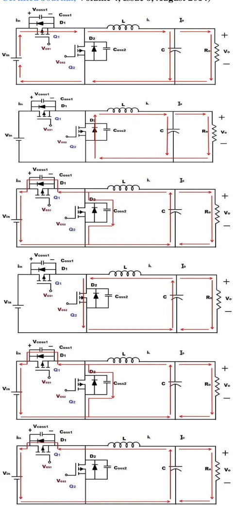
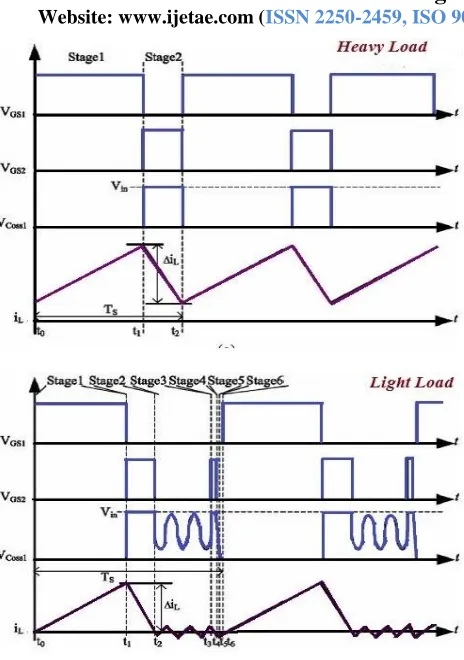
The operation of a SR buck converter grouped into eight stages based on the status of the two switches and load conditions. The oscillograph of the inductor current and control signals in the eight operating stages of an SR buck converter is shown in figure III. Based on the different load conditions whether heavy load or light load and according to the methods introduced here, there are two kinds of operating stage combinations. The first operating stage combination is in the heavy load condition, i.e., Stage 1-Stage 2; whereas the second operating stage combination is in the light load condition, i.e., Stage 1-Stage 6. The following assumptions are made to simplify the analysis.
1. The output load voltage is assumed as constant voltage source due to large output capacitance.
2. No losses occur in any part of the circuit, i.e. all components in the circuit are assumed to be ideal.
Light Load Condition A. Stage 1(t0 -t1):
In this state, the main switch Q1 is turned ON and the SR complementary switch Q2 is made to turn OFF. The path of conduction is shown in figure II.
The inductive current equation is given above is same as that of stage 1 of heavy load condition.
B. Stage 2(t1- t2):
International Journal of Emerging Technology and Advanced Engineering
Website: www.ijetae.com (ISSN 2250-2459, ISO 9001:2008 Certified Journal, Volume 4, Issue 8, August 2014)
533
C. Stage 3(t2- t3):
The current through the inductor has dropped to zero at the time instant t2. To avoid energy losses in the SR buck converter, the SR switch Q2 is made to turn OFF. In this stage, the output inductor L begin to resonate with the parasitic capacitors Coss of switches Q1 and Q2 , which makes Coss1 to be discharged and other Coss2 to be charged.
The inductive current iL(t) and parasitic capacitive voltage vCoss1 can be given by:
Where
D. Stage 4(t3- t4):
[image:3.612.323.563.127.647.2]In Stage 4, the main switch Q1 continued to be turned OFF, while the SR switch Q2 is turned ON. As a result, the voltage across the inductor is vL = -VO , which makes the inductor L to be energized and the inductive current increases linearly in opposite direction.
International Journal of Emerging Technology and Advanced Engineering
Website: www.ijetae.com (ISSN 2250-2459, ISO 9001:2008 Certified Journal, Volume 4, Issue 8, August 2014)
[image:4.612.53.285.116.446.2]534
Figure III. Oscillogram of voltages and inductor current under different load conditions
E. Stage 5(t4- t5):
Stage 5 is the period for resonance. The main switch Q1 and the SR switch Q2 , both are made to turn OFF. The SR rectifying switch Q2 is not conducted while the inductor current should be continuous. This current enables Coss1 to be discharged and Coss2 to be charged, until the voltage across the parasitic capactor Coss1 of switch Q1 is discharged to zero, and the voltage across the parasitic capacitor Coss2 of switch Q2 is charged from zero to a voltage Vin. The inductive current iL(t) and parasitic capacitor voltage vCoss1(t) of switch Q1 are calculated as:
Where
F. Stage 6(t5- t6):
In Stage 6, the main switch Q1 and the SR rectifying switch Q2 are continued to be turned OFF. Though, the parasitic capacitance Coss1 has been already discharged in the previous stage, while Coss2 has been discharged by inductive current. The body diode D1 will be conducted. The zero voltage condition of Q1 has been achieved in this stage. iL(t) and vCoss1(t) of switch Q1 are given as:
According to the previous explanation, the synchronous buck converter is operated in discontinuous mode (DCM) while operated in light load condition. While the inductive current becomes lesser than zero, the SR rectifying switch Q2 continued to be conducted. This will result in the decrease in conversion efficiency of the synchronous buck converter. The SR rectifying switch Q2 is conducted at the second time in one switching cycle makes the main switch Q1 to be conducted with ZVS and increment the efficiency in light load condition. In conclusion, the control method used here has the following merits. Under heavy loads, SR technique is used to reduce conduction losses whereas under light loads, ZVS technique is achieved to reduce switching losses.
III. CONTROL STRATEGY
International Journal of Emerging Technology and Advanced Engineering
Website: www.ijetae.com (ISSN 2250-2459, ISO 9001:2008 Certified Journal, Volume 4, Issue 8, August 2014)
[image:5.612.50.292.113.339.2]535
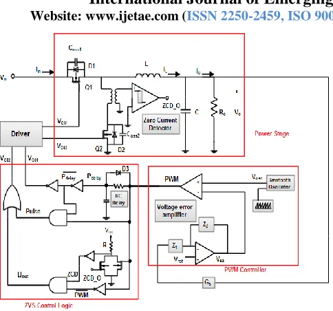
Figure IV: Control circuit structural diagram of an SR buck converter
In the control frame, the PWM controller will be followed by the combination of control logic circuit and RC delay circuit. The dead time control between the switches Q1 and Q2 is carried out by means of driver circuit. The control structure circuit of SR buck converter comprises of two parts. PWM Controller and ZVS Control logic.
PWM Controller
Output voltage is fed back and compared with reference signal to get control signal. This control signal is modulated with saw tooth signal to obtain required PWM
signal.
ZVS control logic
The PWM signal input is first delayed using RC delay (Δt) after double negation forms V
GS1. VGS2 is obtained as
the OR output of two signals U
out and Pulse. Pulse is the
AND output of P
delay and PWM signal. Uout is the AND
output of ZCD and PWM signal. . ZCD will always be
high until inductor current becomes zero. Under heavy load, U
out is influenced by only PWM signal.
IV. PIDCOMPENSATOR DESIGN
[image:5.612.324.573.305.522.2]A buck converter with voltage-mode control and voltage-mode error amplifier can be stabilized with the help of proportional-integral-derivative (PID) compensator. By keeping the ZVS logic circuit apart, the whole circuit can be modeled with three blocks as represented in figure V. The power stage (Gp(s)) includes the power switches, the drivers and the output inductor and output capacitor. The model of the PWM generator is simply represented by 1/ Vosc, where Vosc is the peak to peak amplitude of the oscillator voltage (saw-tooth). The compensator block (H(s)) indicates the error-amplifier with the compensation network.
Figure V:The block diagram model of the synchronous buck converter[27]
Step 1: Calculate the poles and zero of the power stage. Thus the pole of the power stage is at:
The zero caused by the ESR of the output capacitor
Step 2: Select crossover frequency to be 1/8 of the switching frequency. FO =1.25 kHz
Step 3: Select the type of compensator. Since FLC < FO < FESR < Fs /2, Type III-A compensator is suitable for this application.
International Journal of Emerging Technology and Advanced Engineering
Website: www.ijetae.com (ISSN 2250-2459, ISO 9001:2008 Certified Journal, Volume 4, Issue 8, August 2014)
536
The primary zero of the compensator (FZ1) compensates the phase lag of the pole which is located at the origin. The second zero (FZ2) is to compensate for one of the poles of the output LC filter so that at FO the slope of the bode plot of the loop is about -20dB/dec. The second pole of the compensator (Fp2) and the zero of the ESR of the capacitor (FESR) cancel each other and the third pole (Fp3) is to provide more attenuation for frequencies above FS/2.[27]Figure V1. Bode plot of the buck converter power stage, desired loop gain, and Type III-A compensator[27]
Step 5: Calculate the parameters of the compensator. Select Cf3 = 2.2nF. Rf3 is calculated as
Select Rf3 = 45470.24Ω. The Rf1 can be calculated as,
Select RC1 = 446.249kΩ. CC1 is calculated as,
Select CC1 = 1.636nF. Similarly, CC2 can be calculated as
Thus, we get the PID compensator for the SR buck converter with voltage mode control and voltage error amplifier with a transfer function as
The negative sign in the above equation indicates the compensator is present in the feedback loop.
[image:6.612.316.570.410.609.2]V. SIMULATION AND RESULTS
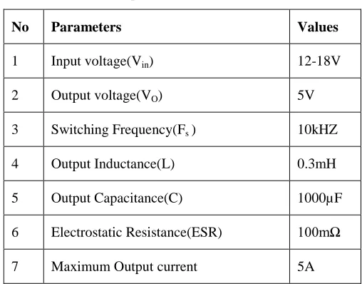
Table 1 shows the model parameters of all elements used for simulation.
Table1
Model parameters and their values
No Parameters Values
1 Input voltage(Vin) 12-18V
2 Output voltage(VO) 5V
3 Switching Frequency(Fs ) 10kHZ
4 Output Inductance(L) 0.3mH
5 Output Capacitance(C) 1000µF
6 Electrostatic Resistance(ESR) 100mΩ
7 Maximum Output current 5A
International Journal of Emerging Technology and Advanced Engineering
Website: www.ijetae.com (ISSN 2250-2459, ISO 9001:2008 Certified Journal, Volume 4, Issue 8, August 2014)
[image:7.612.329.566.104.322.2] [image:7.612.50.292.122.412.2]537
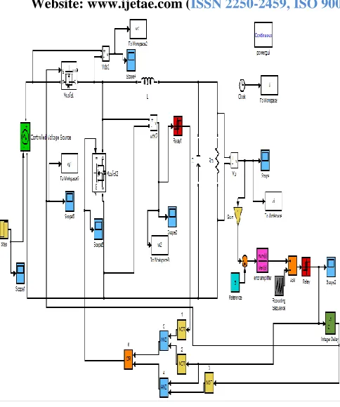
Figure VII. Simulink model for the control of SR buck DC-DC converter with ZVS logic
Figure VII shows the control strategy for SR buck converter with ZVS logic circuit realized in MATLAB Simulink. The input voltage is varied from 12V to 18V using a controlled voltage source. The input voltage given to the power stage is lowered to 5V at the output. This output voltage is fed back and passed through sensor gain and compared with reference signal in the compensated error amplifier (PID compensator) and then modulated with saw tooth signal to generate PWM. This generated PWM is applied as the input to the ZVS control logic circuit. The gating control signals for both switches are the outputs of ZVS control logic.
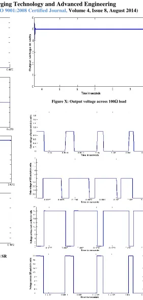
Figure VIII: Output voltage across 1Ω load
The figure VIII and figure IX shows the variations of output voltages,switch voltages and gate voltages with respect to time in case of SR buck converter with voltage mode control and voltage error amplifier using ZVS control logic for load resistance of 1Ω. Since the load resistance is low and this operating condition is also termed as heavy load condition
.
In figure IX, it can be seen that gate voltage of main switch and drain-source voltage of main switch is complementary. That means, the ZVS condition of the main switch is achieved.International Journal of Emerging Technology and Advanced Engineering
Website: www.ijetae.com (ISSN 2250-2459, ISO 9001:2008 Certified Journal, Volume 4, Issue 8, August 2014)
[image:8.612.269.550.104.692.2]538
Figure IX: Gate and switch voltages for main switch Q1 and SR witch Q2 for 1Ω load resistor
[image:8.612.52.296.110.599.2]Figure X: Output voltage across 100Ω load
International Journal of Emerging Technology and Advanced Engineering
Website: www.ijetae.com (ISSN 2250-2459, ISO 9001:2008 Certified Journal, Volume 4, Issue 8, August 2014)
539
Thus, under light and heavy load conditions, the output voltage is kept regulated at 5V for even input voltage variation from 12 to 18V. The ZVS condition of the main switch helps in reducing switching losses with improved light load efficiency.VI. CONCLUSIONS
The PID compensator network for the control strategy applicable to an SR buck converter under any load condition is designed and simulated by analyzing the converter operating principles. Under heavy load condition, SR technique (SR configuration itself) is utilized to reduce conduction losses while under light load conditions; ZVS technique is achieved to reduce the switching losses. This is the control strategy adopted for SR buck converter to operate under any load conditions. This control method has two advantages. First, due to the SR technique, the diode of output rectifier can be replaced by a MOSFET. This will help to reduce conduction losses and increase the conversion efficiency of the converter. Second, when the converter is operated in light load condition, ZVS will be achieved successfully without any auxiliary switch or passive components(R, L, and C). In other words, there is no need to add extra cost in the converter, and thus the conversion efficiency of the converter can also be increased in light load condition. This new control strategy with Type III-A PID compensator has better conversion efficiency than the conventional control technique in light load condition. Simulation is done showing the voltage mode control of SR buck converter stabilized with Type III-A proportional-integral-derivative (PID) compensator and ZVS control logic circuit using MATLAB/SIMULINK.
REFERENCES
[1] Jian Min Wang, Sen Tung Wu and Gwan Chi Jane, “A Novel Control Scheme of Synchronous Buck Converter for ZVS in Light Load Condition", IEEE Trans. on Power Electronics, Vol. 26, No. 11, pp. 3265-3273, 2011.
[2] Master thesis by Muhammad Saad Rahman “Buck Converter Design Issues", Linkping University.
[3] T. Wang, X. Zhou, and F. Lee, “A Low Voltage High Efficiency and High Power Density DC/DC Converter", IEEE Power Electronics Specialists Conference., pages 240-245, 1997.
[4] A. Stratakos,“High-efficiency, low-voltage dc−dc conversion for portable applications", Ph.D. dissertation, Dept. Electrical Engg., Computer Science, University of California, Berkeley, 1999. [5] A. J. Stratakos, S. R. Sanders, and R.W. Broderson, “A low-voltage
CMOS dc−dc converter for a portable battery-operated system,"in Proceedings of Power Electronics Spectrum Conference, Jun. 1994, vol. 1, pp. 619-626.
[6] O. Garcia, P. Zumel, A. de Castro, P. Alou, and J. A. Cobos,“Current self balance mechanism in multiphase buck converter," IEEE Transactions on Power Electronics,vol. 24, no. 6, pp. 1600-1606, June 2009.
[7] X. Zhang and D. Maksimovic, “Multimode digital controller for synchronous buck converters operating over wide ranges of input voltages and load currents,” IEEE Transactions on Power Electronics, vol. 25, no. 8, pp. 1958-1965, Aug. 2010
[8] H. Deng, X. Duan, N. Sun, Y. Ma, A. Q. Huang, and D. Chen “Monolithically integrated boost converter based on 0.5-m CMOS process," IEEE Transactions on Power Electronics, vol. 20, no. 3, pp. 628-628, May 2005.
[9] M. Gildersleeve, H. P. Forghani-Zadeh, and G. A. Rincon-Mora, “A comprehensive power analysis and a highly efficient, mode-hopping DC−DC converter," In Proc. Asia-Pacific Conf. Adv. Syst.Integr. Circuits,,Aug.2002, pp.153-156.
[10] X. Zhou, M. Donati, L. Amoroso, and F. C. Lee, “Improved light-load efficiency for synchronous rectifier voltage regulator module,"IEEE Transactions on Power Electronics,vol. 15, no. 5, pp. 826-834, Sep. 2000.
[11] W. Erickson and D. Maksimovic,Fundamentals of Power Electronics,Norwell, MA: Kluwer, 2001
[12] T. A. Smith, S. Dimitrijev, and H. B. Harrison,“Controlling a dc−dc converter by using the power MOSFET as a voltage controlled resistor,"IEEE Transactions on Circuits Systems,vol. 47, no. 3, pp. 357-362, Mar. 2003.
[13] M. Siu, P. K. T. Mok, K. N. Leung, Lam, Y.-H. Lam, and K. Wing-Hung,“A voltage-mode PWM buck regulator with end-point prediction," IEEE Transactions on Circuits Systems II ,vol. 53, no. 4, pp. 294-298, Apr. 2006.
[14] R. D. Middlebrook, “Small-signal modeling of pulse-width modulated switched-mode power converters,"IEEE Proc.vol. 76, no. 4, pp. 343−354, Apr. 1988.
[15] D. Maksimovic, “A MOS gate drive with resonant transitions,"in Proceedings of Power Electronics Spectrum Conference, June 1991, pp. 527−532.
[16] H.L.N.Wiegman, “A resonant pulse gate drive for high frequency applications,"in Proc. Appl. Power Electron. Conf.Feb. 1992, pp. 738−743.
[17] Y. Chen, F. C. Lee, L. Amoroso, and H. Wu, “A resonant MOSFET gate driver with efficient energy recovery,"IEEE Transactions on Power Electronics,vol. 19, no. 2, pp. 470-477, Mar. 2004.
[18] Z. Zhang, W. Eberle, Y.-F. Liu, and P. F. Sen,“A non isolated Z asymmetric buck voltage regulator module with direct energy transfer," IEEE Transactions on Power Electronics,vol. 56, no. 8, pp. 3096-3105, Aug. 2009.
[19] E. Adib and H. Farzanehfard,“Zero-voltage-transition PWM converters with synchronous rectifier,"IEEE Transactions on Power Electronics,vol.25, no.1, pp. 105-110, Jan. 2010.
[20] H. Mao, O. Abdel Rahman, and I. Batarseh,“Zero-voltage-switching DC−DC converters with synchronous rectifiers,"IEEE Transactions on Power Electronics,vol. 23, no. 1, pp. 369-378, Jan. 2008. [21] H. Bae, J. Lee, J. Yang, and B. H. Cho, “Digital resistive current
International Journal of Emerging Technology and Advanced Engineering
Website: www.ijetae.com (ISSN 2250-2459, ISO 9001:2008 Certified Journal, Volume 4, Issue 8, August 2014)
540
[22] M. Barai, S. Sengupta, and J. Biswas, “Dual-mode multiple-banddigital controller for high-frequency DC-DC converter," IEEE Transactions on Power Electronics,vol. 24, no. 3, pp. 752-766, Mar. 2009.
[23] S. Saggini, D. Trevisan, P. Mattavelli, and M. Ghioni,“Synchronous -asynchronous digital voltage-mode control for DC-DC converters,"IEEE Transactions on Power Electronics,vol. 22, no. 4, pp. 1261-1268, Jul. 2007.
[24] “Designing fast response synchronous buck regulators using the TPS5210," Texas Instruments Incorporated, Dallas, TX, Applicat. Rep. SLVA044, 1999.
[25] I. Pressman , Switching Power Supply Design, 2nd ed.ed. New York: McGraw- Hill, 1999.
[26] AND9135/D: LC Selection Guide for the DC-DC Synchronous Buck Converter.Semiconductor Components Industries, LLC,April 2013.
[27] A.M. Rahimi, P. Part, P. Asadi, “Compensator Design Procedure for Buck Converter with Voltage-Mode Error-Amplifier," AN-1162, International Rectifier.
AUTHOR’S PROFILE
Nivya K Chandran was born in Kerala in 1990. She received the B. Tech degree in Electrical and Electronics Engineering from Vidya Academy of Science and Technology affiliated to University of Calicut, Kerala in 2012. She is currently pursuing her M. Tech Degree in Power Electronics from Vidya Academy of Science and Technology.