1.1 1.2 1.3 1.3.1 1.3.2 1.3.3 1.4 1 .4. 1 1.4.2 1.4.3 1.4.4 1.4.5
1.4.6
1.4.7 1.5 1.6 2.12.1 . 1
2.
1.2
2.1.3
2.1.4 2.22.2.1
2.2.2 2.2.3 2.2.4Physical Description Equipment Supplied Func tiona I Descri ption
Display Modes Timing
CRT Display Options
Character Generator VC38 Character Generator VA38 Slave Option VS38
Search Option VF38 Zoom Option VZ38 Track Balls
Tablets
Reference Documents Specifications
CONTENTS
CHAPTER 1 INTRODUCTION
CHAPTER 2
INTERFACE CONSIDERATIONS Computer I/O System
Program Interrupt Facility
Automatic Priority Interrupt Option DMA Channel
I/o
Skip FacilityVL09/DM09A/PDP-9 Interface Interconnection
Power Requirements VL09 Specifications Signal Description
COI'HENTS (Cont.)
CHAPTER 3 SYSTEM DESCRIPTION
3.1 Display System Registers
3.1.1 Display Address Counter (DAC)
3.1.2 Delta-X Register and Delta-Y Register 3. 1 .3 Pushdown Pointer (PDP)
3.1.4 Initial Conditions Register (IC) 3. 1 .5 Mode Register
3.1.6 Intensity (INT), Scale (SC), and Light-Pen (LP) Registers 3.1.7 X and Y Registers
3.1.8 Pushbutton Flip-Flop Register (PB) 3. 1 .9 Manua I Interrupt Pushbutton 3.1.10 Binary Rate Multiplier (BRM)
3.2 Character Generator Registers (Contained in Option YC38) 3.2.1 Starting-Address Register
3.2.2 Character-Save Register 3.2.3 Character-Address Counter 3.3 PDP-9/339 Data Transfers 3.3.1 Control-State Instructions 3.3.2 Data-State Instructions
CHAPTER 4
OPERATION AND PROGRAMMING INFORMATION
4.1 System Controls and Indicators 4.2 light Pen Operation
4.3 Operator Programming Information
4.3.1 Display Parameters (Coordinate System)
4.3.2 Scale
4.3.3 Intensity Level
4.3.4 State
4.3.5 Mode
4.3.6 Subroutining
4.3.7 Flags
4.3.8 Timing
4.4
4.5
4.5.1
4.5.2
4.5.3
4.5.4
4.5.5
4.5.6
4.5.7
4.6
4.6.1
4.6.2
4.6.3
4.6.4
4.6.5
4.6.6
4.6.7
4.7
4.7.1
4.7.2
4.7.3
A.1 A.1.1A.1.2
A.1.3
CONTENTS (Cont.) Diagnostic Programs
Control State Command Formats Parameter
Mode Jump Pop
Conditional Skip (Bank 1) Conditional Skip (Bank 2) Miscellaneous
Data State Command Formats Point Mode (Two Words) Increment Mode
Vector Mode (Two Words)
Vector Continue Mode (Two Words) Short Vector
Character Mode (Optional) Graphplot Mode
Display Oriented Computer Instructions Group
1 •
From the DisplayGroup
2.
To the DisplayGroup 3. lOT Skip on Display Flags
Control Characters Parameter Control
APPENDIX A
VC38 CHARACTER GENERATOR
Table Control
Miscellaneous Control
APPENDIX B PROGRAMMING EXAMPLES
APPENDIX C REFERENCE TABLES
ILLUSTRA TIONS
1-1 Type 339 Display System, Component Locations 1-2
2-1 Display Interface 2-1
2-2 Interface Cabl ing 2-3
2-3 Interface Signals 2-4
3-1 Type 339 Display, Registers 3-1
4-1 Control Box Panel 4-1
4-2 Type 339 Display, Indicator Panel 4-2
TABLES
1-1 Type 339 Equipment Supplied 1-1
1-2 Type 339 Reference Documents 1-6
1-3 Type 339 Performance Characteristics 1-7
4-1 Controls and Indicators 4-2
4-2 Intensity Scale 4-5
CHAPTER 1 INTRODUCTION
The Type 339 Programmed Buffered Display (Frontispiece) is an on-line system manufactured by Digital Equipment Corporation for operator observation, manipulation, and alteration of computer-stored data. The display system consists of a precision incremental CRT display, display control logic, light pen, pushbutton control box, and interface logic for communication with a PDP-9 computer. The computer processor and the display control logic share the computer memory, and are interdependent as a system.
The computer system furnishes rapid data storage and retrieval for display as dots, lines, curves, or characters (optional) on the face of the CRT. The operator can manipulate or alter the data by using the light pen, pushbutton control box, or the keys and switches on the computer console.
1.1 PHYSICAL DESCRIPTION
The Type 339 system is housed in two standard DEC cabinets bolted together. The cabinets contain the CRT associated circuits and the display logic. Additionally one Type 1943D rack ofmodules comprising the interface logic is installed in the mainframe of the PDP-9 computer.
The display system weighs 900 lb. The dual cabinet measures 69-1/8 in. high, 42 in. wide, and 51 in. deep. When instal led the system must have a 2-ft clearance at a I I access doors and at the sides of the equipment. A minimum clearance of 3 ft is required for remova I of the CRT assembly.
1.2 EQUIPMENT SUPPLIED
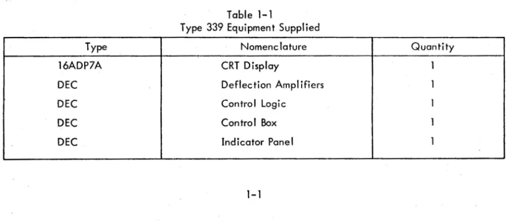
Table 1-1 lists the components of the Type 339 Display System and Figure 1-1 shows the com-ponent locations in the dual cabinet.
Table 1-1
Type 339 Equipment Supplied
Type Nomenc lature Quantity
16ADP7A CRT Display
1
DEC Deflection Amplifiers
1
DEC Control Logic
1
DEC Control Box 1
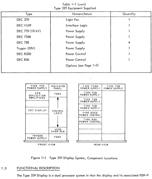
[image:7.620.57.563.27.530.2] [image:7.620.59.556.538.755.2]Table 1-1 (cont) Type 339 Equipment Supplied
Type Nomenc lature Quantity
DEC 370 light Pen 1
DEC VL09 Interface Logic 1
DEC 770 (10 kV) Power Supply 1
DEC 734B Power Supply 1
DEC 728 Power Supply 4
T rygon (50V) Power Supply 1
DEC 832D Power Con tro I 1
DEC 836 Power Control 1
Options (see Page 1-5)
TYPE 770 IN D ICATOR TYPE 7348 TYPE 728
POWER SUPPLY PANEL POWER SUPPLY POWER SUPPLY
339 FANS
DEFLECTION
TYPE 728 POWER SUPPL Y
AMPLIFIERS
TYPE 728 POWER SUPPL Y
TYPE 728 POWER SUPPLY
CRT DISPLAY CONTROL
LOG IC TYPE 8320
POWER CONTROL TYPE 836 POWER CONTROL VC38
CHAR. GEN.
TRYGON FANS
POWER SUPPLY
FRONT VIEW REAR VIEW
Figure 1-1 Type 339 Display System, Component Locations
1.3 FUNCTIONAL DESCRIPTION
The Type 339 Display is a dual processor system in that the display and its associated PDP-9 computer both have processors wh ich operate the computer memory. The on Iy difference is that the dis-play processor (disdis-play control logic) can read information on Iy from memory, but the computer processor can read and write. Using the pushbutton control box, light pen, and computer teletype (optional char-acter mode), the operator can communicate directly with the computer and observe the results of his
[image:8.618.58.554.45.629.2]display processor is controlled from the I/O bus, but receives its commands and data via the direct
mem-ory access (DMA) channel. Associated instructions (display commands and lOT instructions) are stored
in memory. The display file words are loaded into a table or block of successive memory locations; the
beginning address of this table is loaded into a special register called the display address counter (DAC)
and allied break field register (BF). The contents of these registers are applied to the inputs of the
com-puter memory address register (MAL forming a 15-bit address which can increment across memory field
boundaries for access to a total of 32K of memory. A DMA break is then initiated by either the display
or the computer, and the address is read into the MA. The computer then goes into the single DMA
break cycle in which it fetches the word from memory and transfers it from the memory buffer register (MB)
toa buffer register (DX or DY) in the display logic. During this time the display starts its operation and
the DAC is incremented by 1. The computer program counter (PC) is not incremented during the DMA
cycle. At the end of the DMA cycle the computer continues its main program until the display requires
another DMA break.
1.3.1
Display ModesThree groups of fOT instructions permit two-way communication and interaction between the
computer and the display. The first group reads the status of various display registers into the computer
AC register. The second group transfers initializing command information from the computer to the
dis-play, and the third group allows the computer to test registers in the display and perform instruction skips
if certain conditions are met. Among the prestored command words, a mode command initializes the
display to operate in one of seven avai lable modes:
Point Mode:
Increment Mode
Vector Mode
Vector-Continue Mode
Short Vector Mode
Graph-Plot Mode
Positions the electron beam at the point specified by x and y coordinates
Moves the beam from its initial position to any poiht up to 3 bits away in any of eight directions
Displays a line between the initial position and a final position which is located relative to the initial position by DX and DY increments. (The line may be invisible, i.e., not intensified.) ,
Similar to vector mode, except that line is extended through final position to edge of usable picture area .
Same as vector mode but DX and DY packed in one word.
Character Mode (Optional)
1.3.2 Timing
Displays ASCII characters specified by 6- or 7-bit code. Two versions are as. follows.
a. Software - Points comprising each charac ter are stored as subroutines in computer.
b. Hardware - Points are stored in read-only memory in display.
After the display has been initialized and started with the lOT instructions, it requires
mation at a high transfer rate in order to visibly draw the picture. The DMA channel provides the
infor-mation at the required speed. The display timing has been set so that it can request one DMA break
cycle out of five machine cycles, preventing the display from taking too much time from the computer.
This amounts to a DMA break at a maximum rate of once every 6 fJS. In most cases, the display requires more than 6 fJS to process the information, and thereafter obtains a break when more information is
needed. The computer transfers only 12 bits of information at a time to the display. Other high-speed
equipment can
be
used at the same time as the display , by incorporating the optional DMA multiplexerDM09A in the channel so that up to three high-speed devices, including the display, are gated onto the
channel one at a time.
1.3.3 CRT Display
The CRT Display is a 16-inch tube with 9-3/8 in. by 9-3/8 in. usable display area. Magnetic
deflection and focusing techniques result in uniform resolution over this area, described by 1024 bits in
both the X and Y directions, providing approximately 0.01 in. per bit. The X and Y position registers in the display logic are 13-bit registers which can describe 8192 bits in both directions or a 75 in. by 75 in. page. Information can
be
displayed anywhere on this page through a technique called scissoringwhich allows the 9-3/8 in. by 9-3/8 in. screen or "window" to
be
moved anywhere on the page.In-formation can
be
viewed only through this window. The picture being displayed must be in other thanpoint mode and must be a closed loop figure, i.e., after finishing a picture, a vector is drawn back to
the origin. If it is desired to move the picture up, a short vector is drawn before drawing the picture.
The effect of this vector is cumulative and, if it is within the closed loop, it will add each time the
Up to seven display CRTs may
be
remotely slaved to the master CRT, and all can receive identical information, different information, or a combination can be established. The routing of infor-mation to a slave display is a function of display file commands.1.4
OPTIONS1.4.1
Character Generator VC38This option provides the capability for displaying characters on the scope face. The characters are stored in PDP-9 memory as subroutines; the VC38 consists of additional hardware required to dispatch to the subroutines. Average character display time is 50 \JS' If 6-bit character codes are used, they are packed two per 18-bit word; if 7-bit character codes are used, packing is one per word (both versions are right-justified).
1.4.2
Character Generator V A38The VA38 allows the 339 to display one of a standard character set from a read-only memory located in the display. As the character data are in hardware, one character display time is 20 I-IS; pro-: gramming is simplified to a Mode command, followed by 6- or 7-bit character codes.
1.4.3 S love Option VS38
The slave option provides interface, control, and driving circuits that allow up to eight CRT displays, including the master, to use the 339 graphic capabilities. Eight different, identical, or combinations of pictures are possible. The master CRT can be treated as a slave. If not, all pictures sent to all slave units are superimposed on the master CRT.
1.4.4
Search Option VF381.4.5 Zoom Option VZ38
The X and Y registers of the 339 contain 13 bits each. Normally the low-order 10 bits of both are gated to the CRT deflection circuits. Through a manual switch, the zoom option allows the gating of the 10 high-order bits instead of the 10 low-order bits.
1.4.6 Track Balls
Track balls permit the operator to move a mechanical device and cause the picture to rotate in the same direction as the device. The option contains registers wh ich count the movements of the track ball in the X, Y, and Z directions. These registers are read by the computer and implemented in the display file.
1.4.7 Tablets
Tablets consist of a resistive surface from which the X and Y position of a metallic pen can be determined. These positions are temporarily stored in registers and later used by the computer to draw · pictures or position objects on the tube.
1.5 REFERENCE DOCUMENTS
Table 1-2 lists the major documents supporting the 339 Display System.
1.6 SPECIFICATIONS
Table 1-3 summarizes the properties of the 339 Display System.
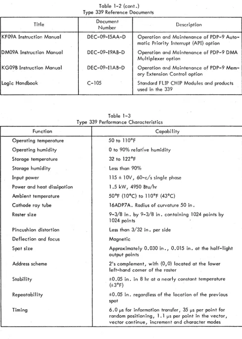
Table 1-2
Type 339 Reference Documen ts
Title Document Description
Number
PDP-9 User Handbook F-95 Operation and Programming of PDP-9
PDP-9 Maintenance Manual F-97 Operation and Maintenance of PDP-9 Instruction Manual
338 Programmed Buffered Display DEC-08-H6AA-D Operation and Maintenance of 338 Display (338 plus VL09 equals 339 Display System)
339 Programming Manual Programming of 339
[image:12.613.54.552.328.688.2]Title
KF09A Instruction Manual
DM09A Instruction Manual
KG09B Instruction Manual
logi c Handbook
Function Operating temperature Operating humidity Storage temperature Storage humidity Input power
Power and heat dissipation Ambient temperature Cathode ray tube Raster size
Pincush ion distortion Deflection and focus Spot size
Address scheme
Stability
Repeatability
Timing
Table 1-2 (cont.) Type 339 Reference Documents
Document
Description Number
DEC-09-JSAA-D Operation and Maintenance of PDP-9 Auto-mati c Priori ty Interrupt (API) option
DEC-09-I9AB-D Operation and Maintenance of PDP-9 DMA Multiplexer option
DEC-09-IlAB-D Operation and Maintenance of PDP-9 Mem-ory Extension Control option
C-l0S Standard FLIP CHIP Modules and products used in the 339
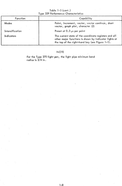
Table 1-3
Type 339 Performance Characteristics Capability
o
to 90% re lati've humidity 32 to 122°Fless than 90%
11S ± 1 OV, 60-c/s single phase 1 .S kW, 4950 Btu/hr
SO°F (10°C) to 110°F (43°C)
16ADP7A. Radius of curvature SO in.
9-3/8 in. by 9-3/8 in. containing 1024 points by 1024 points
less than 3/32 in. per side Magnetic
Approximately 0.030 in., O.OlS in. at the half-light output points
2's complement, with (0,0) located at the lower left-hand corner of the raster
±O.OS in. in 8 hr dt a nearly constant temperature (±3°F)
±O.OS in. regardless of the location of the previous spot
[image:13.615.60.550.47.731.2]Function
Modes
Intensification
Indicators
Table 1-3 (cont.)
Type 339 Performance Characteristi cs
Capability
Point, increment, vector, vector continue, short vector, graph plot, charac ter (2)
Preset at 0.3 f1S per point
The current state of the coordinate registers and all other major functions is shown by indicator lights at the top of the right-hand bay (see Figure 1-1).
NOTE
[image:14.617.63.539.14.739.2]CHAPTER 2
INTERFACE CONSIDERATIONS
2. I COMPUTER I/O SYSTEM
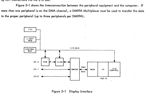
The display, the computer, and their peripheral equipment communicate through the I/O bus and the DMA channel. The I/o bus is used to service relatively slow devices which do not require a high information transfer rate. The DMA channel enables peripheral devices including the display sys-tem to directly access memory in a matter of microseconds. Devices using the channel are controlled by lOT instructions via the I/O bus.
Figure 2-1 shows the interconnection between the peripheral equipment and the computer. If more than one peripheral is on the DMA channel, a DM09A Multiplexer must be used to transfer the data to the proper peripheral (up to three peripherals per DM09A).
OMA CH 1 . . . ---~ OM09A MEM
BUS
[image:15.612.52.551.207.556.2]CH 0
Figure
2-1
Display InterfaceCP
POP-9 I/O CONTROL
2.1.1
Program Interrupt FaciIi
tyThe PI feature of the PDP-9 allows the display to initiate an interrupt of the main program. This releases the main program from the necessity of making repeated flag checks. The PI feature has the lowest priority in the PDP-9 program break hierarchy. Essentially, a program interrupt causes the computer to interrupt its current program operation, store the contents of key registers in assigned memory location 00000, and branch control from location 00001 to a subroutine servicing the I/o device that requested the interrupt. In the 339 display system, any of the following display flags can set the display interrupt flag to cause a program interrupt if the interrupt system is enabled:
2.1.2
Internal Stop External Stop Light Pen Hit Edge Violation Pushbutton Hit Manual Interrupt
Automatic Priority Interrupt Option
The flags listed above may also
be
connected to the "API option if a higher interrupt priority is desired. The API provides four hardware priority levels above the PI priority, and the peripheral flags associated with the display system are normally assigned to API priority level 2 of the four descending order priorities 0, 1, 2, 3.2.1.3
DMA ChannelThe DMA break facility allows the display system to obtain direct access to the PDP-9 memory. This facility has highest priority in the PDP-9 program break hierarchy. Sequenci~g of the DMA break function begins with a break request from the 339 display to the PDP-9 central processor. The direction of data flow is determined in the I/O control section of the computer. The DMA break facility controls entry into the break cycle, generates the necessary control signals to gate address and data into the MA and MB registers respectively of the computer during data input operations, and specifies when data is ready for the display during output operations.
2.1.4
I/O Skip Facility2.2 Vl09/DM09A/PDP-9 INTERFACE
The Vl09 is one rack of logic that is designed to interface between the 338 display and the PDP-9 computer. It uses FLIP CHIP modules of the R, B, and W series and is mounted in the mainframe of the PDP-9. A 339 consists of a V l09 and a 338.
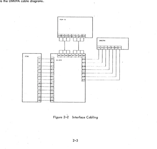
2.2.1 Interconnection
The Vl09 is interconnected as shown in Figure 2-2, using the following cable configurations: Thirteen15-ft coaxial cables from the 339 to the VL09
Two variable-length I/O bus cables from the PDP-9 to the VL09 Seven 10-ft flexprint cables from the DM09A to the V L09
The DM09A connections shown in Figure 2-2 are for DMA channel 2. In instances where the VL09 is to
be
inserted in a channel other than 2 (0 or 1), the correct cable slots con be found by referring to the DM09A cable diagrams." 8
XI -
-X2 --... -x,
X4
X5 x.
n
-X8
x9
>10
XII X3 00
"5
B15
.n 813
.,.
Bl' "7 917
.'6
91.
.'8 .'9
18
POp-g
IIl09
OM09A
.... --_._. -..
-._---- -_._
---_. __ ._--
_._--- - --
[image:17.618.59.559.284.760.2]The VL09 requires the standard FLIP CHIP voltages of +10, -15, and ground. A separate
supply is not needed since the V L09 has less than 20 modules. The power comes from the PDP-9.
2.2.3 VL09 Specifications
The function of the VL09 is to provide the proper polarity signals to the PDP-9 and the display.
In cases where the signals are of the desired polarity, the VL09 either buffers the signal or sends it to its
destination.
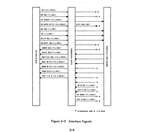
2.2.4 Signal Description
Figure 2-3 shows the signal lines between the display, VL09, DM09A, and the PDP-9
I/o
bus.Brief descriptions for these signals follow.
r - - r - - r
-1M (1Z LINES)
II
RD RO (ILINE)
II
10 ADDR (t 5 LINES)
[0 DATA BITS (12 LINES) A PI-EN2-0UT
II
BK RQ ( I LINE I
IN ( I LINE)
5 KIP RO ( I LI N E)
INTRPT RO II LINE)
II III:
ADDR ACC (ILINE)
'"
'"
II ) (..
u'"
c DATA ROY (I LINE)
:
~~ II: ~
...
w..
...
DEVICE SEL (12 LINES)
..
~0 z
-
::> 2...
...
c'"
BAC IITS (12 LINES) 0...
'"
~ 0> 2
IMI IITS (12 LINES) 0
II
PWR CLR (I LINE)
lOP 1-2-4 (3 LINES)
II
"
10 SYNC (I LINE I
"
API 2 GR (I LINE I
II
10 ADDR (3 LINES I
II
API 2 RO (' I LINE I
"
' - - - ' - - '
-II STANDARD PDP-' 1/0 BUS
[image:18.617.56.560.286.743.2]2.2.4.1 1M Lines - Twleve input mixer lines (1M) originate in the 338 and travel to the YL09 via a
15-ft coaxial cable. From the YL09, the 1M lines are sent to the PDP-9 on the
I/O bus.
2.2.4.2 I/O Address Lines - Fifteen I/O address lines originate in the 338 and travel to the YL09 via
coaxial cable. These lines must
be
inverted from ground to -'JV because the DM09A requires negativelevels for assertion. The
VO
address lines are sent to the DM09A via 10-ft flexprint cabling.2.2.4.3 I/O Data Bits - The I/O data bits (12) are handled in the same manner as the 15
VO
addresslines.
2.2.4.4 RD RQ Line - The read request line originates in the 338 and is sent to the YL09 via the 15-ft
coaxial cabling. The YL09 inverts the negative level to a positive level and sends it to the PDP-9 via
the
I/O
bus. The PDP-9 requires a 1-~s positive pulse to read information into its accumulator. Whenany of the following Read Status commands are given, the RD RQ Itne will go to ground.
RPDP - 700501
RXP - 700502
RYP - 701602
RDAC - 700601
RS4 - 700602
RSG 1 - 700622
RS5 - 701642
RSG2 - 701642
ReG - 701662
RS 1 - 700602
RS2 - 701622
RS3 - 701621
RPB - 700521
2.2.4.5 BK RQ line -The break request line originates in the 338 and is sent to the YL09 via the
15-ft coaxial cabling. The YL09 inverts the positive level to a negative level and sends it to the DM09A
via the 10-ft flexprint cabling. The 8K RQ line tells the PDP-9 that a request for input or output data
has been made by the 338. The 8K RQ line forces the PDP-9 to go into a DMA break· cycle following
completion of the current program execute cycle.
2.2.4.6 IN Line - The IN line originates in the 338 and travels to the YL09 via the 15-ft coaxial
cabling. The signal is then sent to the DM09A via the flexprint cabling. If the signal is at -'JV, data
goes into the PDP-9. If the signal is at ground, data goes from the PDP-9 to the display.
2.2.4.7 Skip RQ Line - The skip request line originates in the 338 and travels to the YL09 via the
15-ft coaxial cabling. The VL09 sends the positive pulse to the PDP-9 via the
I/O
bus.2.2.4.8 INT RQ line - The interrupt request line originates in the 338 and travels to the YL09 via the
WI04 module. The WI04 module sends a PROG INT RQ as well as an API RQ to the PDP-9 via the I/o bus. Either signal will interrupt the program, depending on which interrupt system is enabled.
2.2.4.9 ADDR ACC Line - The address accepted line originates in the DM09AMuitiplexer and travels to the VL09 via the flexprint cabling. The ADDR ACC pulse is buffered and sent to the 338 display. It clears the BK RQ flip-flop and the DX register.
2.2.4.10 DATA RDY Line - The DATA ready line originates in the DM09A and travels to the VL09 via the flexprint cabling. The negative pulse is buffered and sent to the 338 display. It triggers the DATA STROBE and DATA STROBE +0.5 pulses.
2.2.4.11 DEVICE SEL Lines.., Eight device select lines originate in the PDP-9 as negative levels. They are inverted in the VL09, and both polarities are sent to the 338 display. The device select bits gen-erate the I/O code for specific devices.
2.2.4.12 BAC Bits - The buffered AC lines originate in the PDP-9 as ground levels. They are presented to the VL09 via the I/O bus.
2.2.4.13 BMB Bits - The buffered MB bits originate in the DM09A and travel to the VL09 as negative levels. The lines are called AM bits in the DM09A. The VL09 inverts the levels and sends them to the 338.
2.2.4.14 PWR CLR Line - The power clear line originates in the PDP-9 (I/O RESET). It is buffered in the VL09 and then sent to the 338 display.
2.2.4.15 IOPl/2!4 Lines - The input-output pulses 1, 2, and 4 originate in the PDP-9 and are buffered before being sent to the 338 display. These pulses strobe the W103 modules, which produce the lOT pulses in the 338.
2.2.4.16 API EN 2 OUT Line - The automatic priority interrupt enable out line originates in the VL09.
If the 338 is not asking for an API, the line is at -3V. The API EN 2 OUT line goes to the next device down the line via the I/o bus as an enable level. If the 338 is asking for an API, the level goes to ground and the next device down the line is inhibited from asking for an API.
2.2.4.18 API 2 GR - The automatic priority interrlJpt grant line is a negative level generated in the PDP-9 thdt tells the device whether its API request has been answered.
2.2.4.19
I/O
ADDR Lines - ThreeI/o
address lines are generated by theW104 module in the Vl09. If an API request has been granted, the display interrupts to a specific location in memory (00054).CHAPTER 3
SYSTEM DESCRIPTION
3.1 DISPLAY SYSTEM REGISTERS
The 339 Display System control logic contains several flip-flop registers as shown in Figure 3-1
and described below.
r - - - ,
I 1
I I
I I I I I I I I I "8 I I
I
IJJo
,
,
I I I I AC I I I I I I I I I I I"A I
I
I I I I
pOP- 9 I
L
______
-1r---~
I I
I I
INT I I SC
LP
-
c---- r-I
6X 6Y 1-...-0 Y f-.-o
I
I ' - - ~ ~
I
..
,-L
I INT
I
SC BRM
,
LP
I '---:
,
I
-I >
-OAC I
6
I
-I I I
I
I
-I
I
f---t>
IeI
-I
I
I
r----I PTR
'
-I ~ L . . . - PUSH
-I PBr fo- BUTTONS
I
-I 339
CR' ~ X
..
rG
rEJ
ttJ
I I I I I I I I I I I I I I I I I I I I I I I I I ! I I I I~---~
Figure 3-1 Type 339 Display, Registers
3.1.1 Display Address Counter (DAC)
The DAC is the primary address register in the display logic and is used with the PDP-9 DMA
[image:22.615.55.553.176.664.2]Associated with the DACis a 3-bit break-field countup register, which allows the 339 system
to address any of 32,768 words of core memory directly.
3.1.2 Delta-X Register and Delta- Y Register
The b.X register is the main input register of the 339 control. It contains 12 bits and ~ not
a counter. On a DMA break, a data word from the PDP-9 memory is transferred into the b.X register.
From there it is transferred to one or more of the other registers of the control.
During execution of many 339 instruction cycles, information in the
D.X
register is transferred to the b.Y register, which is primarily a holding register. During a point-mode instruction, informationfrom the b.Y register is sent to the Y-position register. Also, the tlY register holds the tlY component of
vectors.
3.1.3 Pushdown Pointer (PDP)
The PTR serves as an address register during 339 subroutine instructions. It isa 12-bit
up-,"
down counter and can be set using an lOT instruction from the PDP-9 AC.
The subroutining structure of the 339 system uses the pushdown list which is located in the first
4192 words of the PDP-9 memory. During push-jump instructions, which obtain entry to subroutines, the
339 status is stored in one word of memory, and the return address from the subroutine is stored in the
next word. If further push-jumps to deeper levels occur, the current status and return addresses are stored in consecutive pairs of words in memory, deepening the list.
Exits from subroutines are called POP instructions. During POP instructions, the PTR is
counted down, and information is retrieved from the pushdcwn list, transmitted to the b.X register, and
from there sent to appropriate registers in the display control.
3.1.4 Initial Conditions Register (IC)
The initial conditions register is a 12-bit register that can be set by an lOT instruction from
the PDP-9 AC. This register contains the information to set up the initial conditions of the 339 display
control, such as enabling interrupts on spec ial flags, setting the drawing size, enabl ing intensification,
etc. The content of the IC register is not read back into the PDP-9 AC, nor is it transferred to any other
3.1.5
Mode RegisterThe mode register is a 3-bit register, which is decoded when data state is active to provide eight operating modes (one is a spare). The modes are point mode (000), increment mode (001), vector mode (010), vector-continue mode (011), short vector mode (100), VC38 character mode (101), grcph-plot (110), and V A38 charac ter· mode (Ill).
3.1.6
Intensity (INT), Scale (SC), and Light-Pen (LP) RegistersThe contents of the intensity register establish the level of picture brightness. The INT regis-ter has three bits. It may be counted up and down and can be set by control state instructions. The de-coded three bits provide eight levels of ihtensification on the screen.
The contents of the sccile register control consecutive dot spacing in the incremental drawing modes. The SC register is a 2-bit up-down counting register, which also can be set or counted by con-trol state instructions.
The light-pen register contains three control flip-flops; LP enable, LP flag, and LP find. If
LP enable is set to a
1 by control-state instructions, this allows
. an LP pulse to set the LP flag and LP find, provided that illumination is detected by the light pen.3.1.7
X and Y RegistersThe X and Y registers spec ify the current electron beam position. These registers are counted up and down in the incremental-drawing modes and are loaded directly from the
llX
andII Y registers in
point mode.If the SC register contains
0,
theX-
and V-position registers are counted only by leach step. If SC contains 1, they are counted by2;
if SC is2,
they are counted by4;
and if SC is3
(maximum), the position registers are counted by 8.3.1.8
Pushbutton Flip-Flop Register (PB)The PB is a 12-bit register associated with the pushbutton control box. The PB can be set via an lOT instruction with information from the PDP-9 AC. It can also be read back into the AC. The contents of the PB are indicated on corresponding lighted buttons on the pushbutton control box.
3.1. 9
Manual Interrupt PushbuttonWhen the mar:lual INTERRUPT pushbutton on the control box is depressed, it causes an interrupt request to be generated in the 339 logic. If the PDP-9 interrupt system is on at this time, an interrupt of the PDP-9 program occurs. Depressing this button does not stop the display.
3.1.10
Binary Rate Multiplier (BRM)The BRM is a lO-bit up counter with a logic configuration designed to produce pulse trains. It is a major component in the vector-generating logic. During a vector sequence, the AY and AX registers are loaded with the vector information, and the BRM is counted from 0 through octal 1777 bock to O. The transition from all lis back to 0 signifies the end of the vector.
3.2 CHARACTER GENERATOR REGISTERS (Contained in Option VC38)
These registers are associated with character generation:
Starting-address register (SAR) Character-save register (CS) Character-address counter (CHAC)
The character generator uses the dispatch-table technique for drawing characters; that is, a 6- or 7-bit character code represents the least significant bits (LSB) of an address. When this address is referenced in the PDP-9 memory, a word is transmitted to the display. Th is word may
be
the starting address in memory of the character itself, that is, the character represented by the 6- or 7-bit code, orit may
be
a control word, such as escape-from-character-mode, or a carriage return.Characters are drawn in either the increment mode or the short-vector mode. Therefore, they can
be
any length and any shape, and are terminated by an escape from the increm"ent, or short-vector, mode back to the character mode.3.2. 1
Starting-Address RegisterThis is a 6-bit register (not a counter) which is used with the character code to determine the initial reference in the dispatch table.
3.2.2
Character-Save Registersix bits of the computer word represent the first character, and the rightmost six bits of the computer word represent the second character. Thus, while the first character is being drawn, the second charac-ter code is saved in the CHSR.
3.2.3 Character-ll.ddress Counter
This IS-bit register is used precisely as DAC is used, except that it is limited to character generator operations. It is an up-counter and references consecutive addresses in core memory during execution of the characters.
3.3 PDP-9/339 DATA TRANSFERS
The PDP-9 registers affected by the DMA break system are the MB register and the
MA
register. A. third register, the PDP-9 AC, is used with theVo
bus to load initial parameters into the 339 registers, and also to read PDP-9 status back into the A.C under program con.trol. The DMA-break logic is described in thePDP-9 Maintenance Manual.During a break, one of the 339 address registers loads the MA register. The break system uses such address information to read a word from memory into the MB register for transfer into the 339 llX and lC registers. Only the llX and IC registers are loaded from the MB.
During a push-jump instruction, data from the 339 registers returns to the MB register to
be
stored in the pushdown list in memory. This information consists of light-pen status and scale, intensity, and mode information, the 3 bits from the break field counter, and the 12 bits from the DAC.
During a POP instruction, this status and return-address information is transferred from the MB into the llX register, from which it is returned to the break-field, DAC, light-pen status, scale, intensity, and mode registers.
3.3.1 Control-State Instructions
Chapter 4 describes data transfer between the 339 registers on an instruction-by-instruction basis. In control state, display instructions are executed in a manner similar to computer instructions. Each instruction has an OP code that determines the logic operations to
be
executed. These are either one- or two-word instructions and require from one to four break cycles for execution.3.3.2 Data-State Instructions
The display is always in control state at the start. To enter data state, a control-state
instruction must first be executed. A parameter instruction with bit 17=1 or POP instruction with bit 17=1
causes the display to enter the data state.
The instructions available in data state differ in operation from those in control state in a
sig-nificant way. The instructions in data state do not have OP codes such as those assoc iatcd with
instruc-tions in control state. For this reason, the 3-bit mode register is set before entering data state. There
are eight possible modes.
Once the display control enters data state; for instance in mode 0 (point mode), each pair of
words taken from memory is treated as a point-mode instruction until the escape bit is set in one of the
word pairs. The escape bit causes the display to return to control state. Control-state instructions are
then executed until the system reenters data state in the execution of a control-state command code
or 3.
In data state, the cycles are called 51 and 52. The two-word modes are point mode, vector
mode, and vector-continue mode. In 51 the first word is read from memory; in 52 the second word is
read. When the instruction is executed, the operation reverts to 51. In the one-word modes, which
CHAPTER 4
OPERATION AND PROGRAMMING INFORMATION
This chapter describes system controls and indicators and furnishes information on the display system operating procedures.
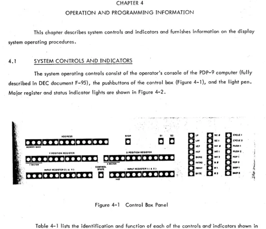
4.1 SYSTEM CONTROLS AND INDICATORS
The system operating controls consist of the operator's console of the PDP-9 computer (fully described in DEC document F-95), the pushbuttons of the control box (Figure 4-1), and the
I
ight pen. Major register and status indicator lights are shown in Figure 4-2.aODUSS STOP
c
c c
Y POSITION REGISTU X POSITION RtOISTER
Of
i
Ilk
i
1](
i
1)(
i
it
Ok
I
Il[
X X]( I
i
j(I
i ,
_
, stCtOI! II.IIc:ro.
INPUT .£015T[R 2 ( ' ,. I
CONTROL
STATI . 1NPUT R(GISlER 1 ( , X) ,.,':
C
f i
I )( X I )( I
i )( i
I ]
,
;
:
It.t.,
C
-
I Xu X 1]( I
I ](
X I
1
Figure 4-1 Control Box Panel
[]t.
[]sc,
[ ] m [ ] set
[ ] YEt [ ] INT ,
[ ] ME.' [ ] INT 1
C··
1tO[ l
...
[ l
INlltO ..[ l
III •
[l'I",' [l.'
:
[]m •
.
[] ••
[ ] CYc:LI'
[ ] CYCLE' [ ] PUSHt [ ] PUSH 2 .
[ ] POP 1
[ ] pop,
8'·'"
_ ITable 4-1 lists the identification and function of each of the controls and' indicators shown in these Figures 4-1 and 4-2.
The control panel illuminating type pushbuttons are arranged in two banks of six. Each bank can be reset by depressing the associated clear (CLR) button. Within a bank of six only one can be pressed because of mechanical interlocking, but single buttons from each bank can be pressed simulta-neously. Complementing flip-flops are associated with the pushbuttons of the pushbutton logic. A
pushbutton is lit when the flip-flop is in the 1 state.
[image:28.617.38.561.49.498.2]Switch
0-11
INTERRUPT
Light
MEMORY BANKADDRESS
STOP
S 1, S2
Y SECTOR
Y POSITION REGISTER X SECTOR
X POSITION
INPUT REGISTER 2 (6Y) CONTROL STATE
Figure 4-2 Type 339 Display, Indicator Panel
Table 4-1 Controls and Indicators
Control Box
Function
Switches are associated with flip-flops PBFO-11 , respectively. Push ing a button causes a pushbutton hit flag.
Provides a manual interr.upt fac i lity. Indicator Panel
Function
Three binary indicators that identify the 4096-word memory field being addressed
Display 15 bits (including MEMORY BANK) of current mem-ory address
Indicates external stop flag on
The two cycles used in data state, when infprmation is pre-sented to the CRT
State of 3 bits that provide sector addressing of 8 Y sectors* State of 13 bits that provide direct address of 8192 Y points* State of 3 bits that provide sector addressing of X sectors* State of 13 bits that provide direct address of 8192 X points* Indicates content of 6Y register
[image:29.618.57.553.46.744.2]Light
INST
INPUT REGISTER 1 (6X) LP LPF VEF HEF BKRQ INTRQ PBHIT BYTE SCO SCI INTO INTI INT2 MO Ml M2 CYCLE 1 CYCLE
2
PUSH 1 PUSH 2 POP 1 POP
2
SKIP
1
SKIP 2
*See Section 4.3.2.
Table 4-1 (cont.) Controls and Indicators
Indicator Panel (Cont.)
Function
Condition of 3 most significant bits of INPUT REGISTER 1 (identify current instruction).
Indicates content of 6X register Indi cates
I
igh t pen on (enabled) Indicates light pen find flagIndicates vertical edge flag (overflow or underflow in the Y register)
(6X)
Indicates horizontal edge flag (overflow or underflow in the X register)
Indicates DMA break request is active Indicates an interrupt request is active Indicates pushbutton hit flag is on
Indicates that the first byte .of a word in the increment mode has been executed.
State of scale register bit 0* State of scale register bit 1* State of intensity bit 0
State of in tensi ty bit 1 Intensity bits provide selection State of intensity bit 2 of B intensity levels
-.
Mode bit
0
Mode bitl Mode bit
2
Indicates whi ch of eight control state cycles is about to be executed
Indicates conditional skip 1 active
Indicates conditional skip
[image:30.614.61.548.50.732.2]4.2 LIGHT PEN OPERATION
By using the light pen, the operator of the CRT displcty call COfllllltJllicalt' imllwdinlcly wil"
the PDP-9processor. The light pen is an input device that generates a signal (flag) that can be sensed
and interpreted by the computer • When the light pen is positioned over agraphic and senses light,
dis-play operation ceases with the control logic retaining the X and Y coordinates at the point of light pen
interruption. The light pen strike alerts the program via program interrupt or automatic priority interrupt,
if the light pen flag enable bit hqs been previously set.
4.3 OPERATOR PROGRAMMING INFORMATION
The PDP-9 input-output transfer (lOT) instruction scheme provides computer communication with
the I/O equipment, and the display is an I/O device to the computer. These lOT instructions, summarized
in Paragraph 4.7, control initialization of the display, sense the state of the display, and restart the
dis-play after an interrupt.
Any portion of PDP-9 core memory can
be
reserved for display instructions which are arrangedin core memory and constitute a display program. This arranger:nent can be either sequential or
non-sequential (jumps). Instructions are transferred to the display system on demand by the display system via
the PDP-9 DMA break facility.
Once it is started, the display control operates through the DMA break facility to fetch
in-structions (display program) to generate the raster. When the graphic is constructed, the last instruction
in the sequence can
be
coded to stop operation. The subsequent program interrupt or automatic priorityinterrupt notifies the computer that the graphic is completed and the system is ready for further direction.
In normal computer programming, a program can call a subroutine to execute repetitive
op-erations. Similarly, the display PUSH JUMP and POP instructions add subroutining'capobility for
graphics. If a particular graphic, for example, a circle is to
be
drawn in many locations on the CRT,it is advantageous to use a single display instruction sequence to construct the circle each time.
There-fore, whenever the circle is repeated, the same display sequence is called by the subroutine call display
instructions. The display instruction repertory enables open and closed subroutine calls. Multi level
sub-routines are likewise possible.
4.3.1 Display Parameters (Coordinate System)
The display screen is 9-3/8 in. square and has 1024 points in the X and Y directions (10 bits
for X and 10 bits for Y), or about a million points. The X- and V-position registers are 13 bits long,
however, so the screen represents only 1/64 of the total addressable area (paper). The paper is broken up
Only information in sector 0 is intensified, so that translation is accomplished by moving the picture
(or graphics) in relation to sector 0. The lower left corner is point (0,0), and the coordinates increase
"C the right and up to the upper righ t corner (1777
8, 17778),
An edge violation occurs when a line is drawn across the boundary of the paper. This is an
indication that an overflow or underflow condition has just occurred in the X- or V-position register. The horizontal edge flag indicates overflow or underflow in the
X
register; the vertical edge flag in-dicates overflow or underflow in the Y register. The overflow can be set to occur after the 10th, 11th,12th, or 13th bit in
X
andY.
The effective paper size can therefore be changed under program control.4.3.2 Scale
The scale setting determines the number of positions each succeeding spot is moved before
becoming intensified. It affects both the size and appearance of lines or symbols drawn in the vector,
vector-continue, short vector, increment, and character modes'. At scale setting 11
2, each point can be clearly distinguished. At scale setting 002' line and symbols appear to be continuous. The point
spacing is illustrated in Table 4-2.
Scale
°°2
•
•
•
01
2
•
0•
1°2
•
0 0112
•
0 04.3.3 Intensity Level
Table 4-2 Intensity Scale
Point Spacing
• • • •
0
•
0•
0
•
0 00 0 0 0
Intensify
•
•
•
Every0
•
0 2nd0
•
0 4th0
•
0 8thEight intensity levels are available on the display, ranging from 0002' which is barely visible,
to 111
2, which is very bright. Scale and intensity settings are interrelated. If characters are drawn (using the character generator) at the lowest scale setting, and too high an intensity level is used, the
characters blur badly. On the other hand, if many characters are to be displayed simultaneously, or if
the light pen is to
be
used, it is best to use as high an intensity level as practical. Intensity level 1002 is normally bright enough for light pen operation.4.3.4
The display logic is divided into two sections: data state and control state. Control-state
[image:32.620.38.565.54.673.2]commands are instructions to move the beam via the X- and Y-position registers. When the display is
initialized, the commands are accepted in control state until an enter-data-state command is given.
The display returns to control state from data state by escaping. (An escape bi t in the last data state
command signals the display logic to return to control state.)
In control state, the first three bits (op code) designate the operation to be performed by the
remaining nine bits. All eight op codes are used:
o
ParameterMode
2
Jump3
POP4 Conditional skip 1
5 Conditional skip 2
6 Misce"aneous (microprogrammed)
o
Arithmetic compare 1 Arithmetic compare 22 Skip on flags
3 Count (scale and intensity registers)
4-7 Set slaves (optional)
7 AC line voltage synchronization
4.3.5
ModeData-state words are accepted in one of seven formats defined by the contents of the mode
register. The data-state modes are as follows.
0 Point
Increment
2
Vector3
Vector continue4
Short vec tor5
Character (optional), VC38 6 Graphplot7
Charac ter (optional), VA38All these modes are entered from control state by the enter-data-state command. Each mode I
however I has its own way of escaping back to control state. The mode register is cleared by the system
I
4.3.6 Subroutining
The display has control-state commands that can modify the DAC. This flexibility enables uncondi tional display jumps (J UMP) ,. jumps to subrouti ne (PUSH JUMP) ,and re turns from subroutines (POP). The new address is specified by 15 bits which allows direct addressing of 32K of core memory. The JUMP and PUSH JUMP commands are specified by two consecutive 12-bit words. PUSH JUMP stores the return address, mode, intensity, scale, and light pen status on a pushdown pointer list which resides in the first 4K of the PDP-9 core memory. This information is automatically written into two locations in the format shown be low.
light
Break Field Pen Scale Mode Intensity
EnablE
6 7
8
9 10 11 12 13 14 15 16 17First Word
Low Order 12-Bi ts of Memory Address
6 7
8
9 10 11 12 13 14 15 16 17Second Word
The information is placed in the address indicated by the pushdown pointer (PTR), which is a 12-bit register in the display logic. When a PUSH JUMP is executed, the PTR is incremented twice, adding a new entry to the PTR list. This allows multilevel and recursive subroutines in the display.
The POP command reads the last entry on the PTR list from core memory and gates it back to the appropriate registers. The display status can be inhibited, however, from being restored. The PTR is decremented twice during the POP instruction, making the pushdown list a last-in first-out stack.
4.3.7
FlagsSeveral special conditions arising in the display often require the attention of the PDP-9 processor. These conditions cause display flags that can interrupt the computer. The states of display flags are sensed by lOT skip instructions. The flags are as follows.
c. Edge d. Light pen e. Pushbutton hit
f. Manua I interrupt
The flags can ce sep:::rated into two groups. Flogs le\ ~f-ro'..'~~
-:!
:
~'cc tk,<? -:;Jisc!-;,i ncgs ('")and (f) do not stop the display. Group I flags are cleared in one of three ways: initialization of a dis-play sequence (lOT 1605); resuming from the point the disdis-play stopped (lOT 0724 or lOT 1604); and issuing a pulse to clear the flag if the display is no longer needed (JOT 1601). Power clear clears all display flags.
4.3.7.1 Internal Stop - Internal stop is set by a control-state command (1400). When the display stops, the DAC is already incremented and points to the location that follows the stop code. The PDP-9 skips, if the internal stop flag is ~n and lOT 0721 is executed. Execution of lOT 1604 (with the AC==O)causes the display to resume from this point.
4.3.7.2 External Stop - The PDP-9 lOT 0704, with AC bits 6 and 10 at 0, causes the display to stop. When the display stops, the external stop flag is set, interrupting the computer if the interrupt ·system is on.
The time lapse between the lOT and the display stop is dependent upon the display command being executed when lOT 0704 was initiated. This entire command is executed before the display stops. If the command is a two-word instruction jump, vector, or point-mode command, bath words are
exe-cuted before the display stops. This allows simple resumption of the sequence, even if the display is used in the interim.
The external-stop flag causes the PDP-9 to skip when lOT 0701 is initiated (with AC bits 6 and 10 at 0). The display sequence can be resumed by initiating lOT 0724.
4.3.7.3 Edge - The edge is defined as the point at which the X- or V-position registers overflow or underflow. The initial conditions of the display can be set so that 01 I edges are ignored. In normal usage I the edge flag stops the display; when the edges are ignored, however, the display waits 35 ~s and then resumes automatically. lOT 0724 restarts the display from the edge I if the display stops. lOT
0702 causes the PDP-9 to skip, if either the horizontal or vertical edge flog is on.
If an internal and external stop occur at the same time, only one of the stop flogs is setac-cording to the relative occurrence times.
4.3.7.4 light Pen - The light pen flog stops the display when set by the light pen pulse. This occurs about 6 J.lS after the initial flash. The display logic, therefore, has time to execute several more points in the vector before it stops. The PDP-9 can skip on the light pen flag using lOT 0642. The vector or increment sequence can be resumed by using lOT 0724.
4.3.7.5 Pushbutton Hit - If any of the twelve pushbuttons are hit, the pushbutton hit flog is raised. Th is flog does not stop the display, but can cause a computer interrupt. The flog is cleared by lOT 0602, which reads back the status of the flag into the AC. lOT 0621 reads the state of the twelve pushbuttons into the accumulator. There is no skip lOT for the pushbuttonhit flag.
4.3.7.6 Manual Interrupt - The manual interrupt flag is set by the interrupt button on the pushbutton box . This isan illuminating pushbutton, so that the button is lit whenever the flag is set. This flog does not stop the display. The flag can be cleared by lOT 0722, which also causes the program counter to skip, if the flag is set.
Four of the display flags must be gated onto the interrupt line by the initial condition lOT 0665. These flags are edge, light pen, pushbutton, and internal stop. The external stop and manual interrupt flags always cause an interrupt, if the interrupt system is' on.
4.3.B Timing
The display can take a DMA cycle at the maximum rate of one out offour memory cycles (once each 5.0 J.ls). This rate is maintained, if control state instructions are being executed;* All con-trol state instructions except JUMP, PUSH JUMP, and POP are executed in one display cycle. The JUMP instruction requires two cycles because it is a two-word instruction. The PUSH JUMP is a four-cycle instruction: two four-cycles to get the instruction out, and two four-cycles to push the two status words away on the pushdown list. The POP instruction is a three-cycle instruction: one cycle to obtain the instruction and two to read the status words from the pushdown list.
The VC38 Character Generator (optional) plots at approximately 50 fJS per character. This time is variable, depending on the number of intensified points in the character. Control characters ore executed in two display cycles, except for carriage return which takes an additional 35 fJS.
To estimate the time required to display a character, add up the time required for drawing the character, then add in 12fJs for a 6-bit character dispatch and 14 fJS for a 7-bit character dispatch.
4.4 DIAGNOSTIC PROGRAMS
Diagnostic programs, designed to test specific functions within the PDP-9, are available and described in the PDP-9 Maintenance Manual. These include system input/output tests and MAINDEC routines to check the processor and core memory operation.
In addition, the diagnostic routines listed in Table 4-3 are designed to test specific functions within the 339 System. These, and the PDP-9 MAINDEC routines, are avai lable as perforated paper tapes in readin mode (RIM) format. Each diagnostic routine tape is accompanied by a description of the program, procedures for using the program, and information on analyzing the program results to locate specific failures. Application of these routines are indicated at appropriate points in Chapter 4 of the PDP-9 Maintenance Manual, as they apply to preventive and corrective maintenance of the Type 339 System.
Table 4-3
Type 339 System MAINDEC Programs
MAINDEC Number Title Description
9A-D6JA-D Push Jump Test T est Push Jump instruction
9A-D6KA-D POP Test Tests Pop instruction
9A-D60A-D Lots of Little Pictures on Used for adjusting .analog
the 9 subsystem
9A-D6NA-D VIS Buffer Test Tests data state, primari Iy 9A-D6MA-D Instruc tion Test Tests control state, primarily 9A-D6QA-D Character Generator Test Tests character generator
function (VC38) 9A-D6LA-D 339 Push button Test Tests Pushbutton Skip
instruction
4.5 CONTROL STATE COMMAND FORMATS
[image:37.618.54.557.174.669.2]for each function. If the enable bit is a 1, the associated register is reset to the appropriate value. If the enable bit isa 0, the associated register is unchanged independent of contents of the bit(s) following the -enable bit. There is no restriction on the number of registers that can be changed with one instruction.
4.5.1 Parameter
Op Code:
Scale light Intensi ty
Parameter Pen
6 7 8 9 10 11 12 13 14 15 16 17
0 0 0
Parameter command is an instruction to change the scale, light pen, and intensity registers. When the light pen register is a I, a light pen hit stops the display. If the light pen register is a 0, all light pen hits are ignored.
Bits 6-8
9
10, 11 12 13
14
15, 16, 17
Mnemonic Symbol LPOF LPON SCI SC2
Op code: parameter Enables sca Ie change
Interpretation
Determines one of four passible scale settings if bit 9 is a 1 Enables light pen change
Turns the light pen on when it is a I, or off when it is a 0, provided bit 12 is a
1
Enables intensity change
Determines one of eight possible intensity settings if bit 14 is a
1
ASSOCIATED MNEMONICS AND VALUES Octal
Operation Code
0040 light pen off
0060 light pen on
0400 Set scale to XI
ASSOCIATED MNEMONICS AND VALUES (cont.)
Mnemonic Octal
Operation
Symbol Code
SC4 0600 Set scale to X4
sca
0700 Set scale toxa
INT* 0010 Set the intensity
*INT enables only the change of intensity; a space then a number between Oand 7 to indicate the de-, sired intensity should follow. Any of the mnemonics of the same op code may be combined to form a compound command. Atypical parameter command would be SC2 LPOF INT 4 wh ich would have an octal value of 554.
4.5.2 Mode
Clear
Clear Clear Enter
Op Code: Stop
Push-Mode Sector Coord- Data
Mode Code Button
Bits inate State
Flag Bits
6 7
a
9 10 11 12 13 14 15 16 170 0 1
The mode command has six separate functions. It can cause the display to stop and set the internal stop flag, clear pushbutton flag, set the mode register, clear sector bits, clear coordinate bits, or enter data state. Only the mode change has an enable bit to prevent its being changed.
Bits
6, 7, 8
9
10
11
12, 13, 14 15
16
17
Interpretation
Op code: mode
Stops the display and sets the internal stop flag when bit is a 1 Clears the pushbutton and manual interrupt flags when bit is a 1 Enables mode change
Determines one of eight possible mode settings if bit 11 is a 1
Clears only the high-order three bits in both the x- and y-position registers when bit is a 1
Clears only the low-order 10 bits in the x- and y-position registers when bit is a
1
ASSOCIATED MNEMOr--HCS AND VALUES
Mnemonic Octal
Operation
Symbol Code
EDS 1001 Enter data state
CCB 1002 Clear coordinate bits
CSB 1004 C I ear sec tor bi ts
POINT 1100 Set mode to 0
INCR 1110 Set mode to 1
VEC 1120 Set mode to 2
VECON 1130 Set mode to 3
SVEC 1140 Set mode to 4
CHAR 1150 Set mode to 5
GRAPH 1160 Set mode to 6
ClDF 1200 Clear flag
STOP 1400 Stop display
4.5.3 Jump
Op Code:
Scale light Push Break Field
Jump Pen
6
7 8 9 10 11 12 13 14 15 16 170 1 0
First Word
low Order 12 Bi ts of Address
6 7 8 9 10 11 12 13 14 15 16 17
Second Word
Bits
6, 7,
a
910, 11
12
13
14
15, 16, 17
Second Word
6, 7, 17
Mnemonic Symbol
JUMP
PJMP
LPOF
LPON
SCI
SC2
SC4
sca
Op code: jump
Enables scale change
Interpretation
Determines one of four possible scale settings if bit 9 is a 1
Enables light pen change
Turns the light pen on when it is aI, or off when it is a
0,
provided bit 12 is a1
When bit is a 0, the command is a simple jump, the scale and light pen are changed, and the new IS-bit address is inserted in the DAC and the display continues from there. When bit is aI, the command is a push jump. The old address and the status of the display are stored on the PTR list; then the new address and scale or
I
ight pen change is inserted.Specifies the high-order
3
(of 15) address bits for the jump or push jump commandSpecifies the low-order 12 (of 15) address bits for the jump or push jump command
ASSOCIATED MNEMONICS AND VALUES
Octal
Operation Code
2000 Jump to IS-bit address
contained in last digit and the next word addressed
2010 Jump to subroutine
ad-dressed the same as JUMP
0040 Light pen off
0060 light pen on
0400 Set scale to Xl
0500 Set scale to X2
0600 Set scale to X4