4e:;5-608 10/2/84
AU ?63
XR
United States Patent
[19]McLean et
ale
[54] FREQUENCY·INDEPENDENT,
SELF-cLOCKING ENCODING TECHNIQUE AND APPARATUS FOR DIGITAL
COMMUNICATIONS
[75] Inventors: Peter T. McLean; O. Winston Sergeant, both of Colorado Springs, Colo.
[73] Assignee: Digital Equipment CorporatiOll,
Maynard, Mass.
[21) AppJ. No.: 301,193
[22] Filed: Sep. 11, 1981
[51) Int. 0.3 ... H04L 25/49 [52] U.s. O ... 375/17; 371/56; 375/19;455/608 [58] Field of Search ... 375/17, 19,20,37, 375/55,60, 110; 332/11 R; 371/56; 370/43,44; ,
360/40,41,44,45,48,51; 455/608
[56) References Cited U.S. PATENT DOCUMENTS
Re. 31,311 '7/1983 Miller ... 360/40
3,243,S80 3/1966 Welsh ... 360/42 3,276,033 9/1966 Cogar et aI ... 360/40 3,331,079 7/1967 Reader ... 360/40 3,840,892 10/1974 Hayashi ... 360/4S 3,863,02S 1/197S Gonsewski et aI ... 37S/SS 4,027,1S2 S/1977 Brown et aI ... 4SS/608
4,084,069 4/1978 Looschen ... 37S/17 4,167,760 9/1979 Decker ... 360/40
4,2SS,742 3/1981 Gable et aI ... 37S/19
4,282,601 8/1981 Flora ... 37S/17 4,317,211 211982 Quesnell ... 37S/87
OTHER PUBLICATIONS
Logic Diagram-Transceiver, Model T550 (Network Systems Corporation)-2 pages.
J. Norton, "Drop Your Costs, But Not Your Bits With
NRZ
DATA
ENCODED
DATA
., .
.,.. -,',
o
[11]
Patent Number:
[45]
Date of Patent:
4,475,212
Oct. 2, 1984
a Manchester-data Decoder," Electronic Design 15, Jul. 19, 1979 at 110-116.
Taschenbuch Der Nachrichten-Verarbeitung Unter Mitwirkung Zahlreicher Fachleute Herausgegeben Von Dr. Ing K. Steinbuch Springer-Verlag Berlin!-GottingenIHeidelberg, 1962.
Primary Examiner-Benedict V. Safourek Attorney, Agent, or Pirm-Cesari and McKenna
[57] ABSTRACT
A self-clocking encoding technique for synchronous transmission of digital signals, and apparatus therefor. In an exemplary embodiment, the encoding technique utilizes relatively positive and negative pulses of fixed, predetermined duration. For electrical pulses, the point of reference is preferably a zero baseline. At the leading edge LEi of the i/" bit cell, the value of the i/" bit is encoded as a positive pulse in the case ofa logical "I" or a negative pulse in the case of a logical "0". Further, the next subsequent (Le., (i
+
1)1" bit has the same value, a pulse (e.g., 82D) of the opposite polarity is injected into the i'" bit cell after the leading edge pulse. Thus, positive and negative pulses alternate and the informa-tion content of the encoded signal has no d.c. compo-nent; this facilitates a.c. coupling. Further, the encoding technique is bit-rate (i.e., frequency-) independent and usable over a wide range of bit transfer rates. The re-ceiver can synchronously decode the signal if it knows the pulse width; it need not know the sender's transmis-sion rate and indeed, bit transmistransmis-sion rate may even change from one bit cell to the next.
For a fiber optic implementation, a non-zero baseline is used. The optical zero output level replaces the electri-cal negative pulse level, the half-maximum optielectri-cal out-put level replaces the electrical zero level and the maxi-mum optical output level replaces the electrical positive pulse.
14 Claims, 9 Drawing Figures
o
o
-~
1
-I
t
'1.,
\
u.s.
Patent
Oct. 2, 1984
.~
l(
Sheet 1 of 7
~---~---
"\
(
T
I-CD
-t
1-10--t
I-V-t
~
-i
1-'"--t
-
I--.J:
o
o
o
o
CD
Nc:(
a:!;i
Zo
I
o
~~
Oct
Uo
Z iLl
CD
N
CD
o
If)
.,
o
N
"---4,475,212
iLl
>
a:
0
0
'---a:
w
..J
c5
a:
I-Z
r---
---,
I
I
I
I
I
(04
T
_
I
r---,
~2
1
106,
I
I
__ ,-1
II
"
LI_' _"' ___ _
X
172
1---,
1
-=
I1
X Y+
I
2 I
MUX
~
,..-,
III'
rl-r-<rl:
I'
r
II I
X
3 y-
~J!:~
I :
112C
t---,.--:.I- "
-..,-~
ColENA
l.:
I I112
---.-:..-..Jl~OATAI
I
~-~
t
I
I
~ ~
--,
I :1 1
I
: :
I
J---+-~--ID
Q
-5.2
I
1
I
DEL.
DATA
I I
" _
I
164
I L---C----
J
L
110
-5.2
I'108
---~
Fig. 3
c
•
CIl
.
~
~
(1)
::s
f""to-o
(")
r-,!'-)
-\0
00
~
en
::r
~ ~
...
N
o
....,
-...J~
--
~-.l
til
--
N
~
[image:3.820.191.760.22.495.2]u.s.
Patent
Oct. 2, 1984
Sheet 3 of 7
4,475,212
---
--
--- --- --- --- ---
-
--:r
u ~~
~
~
~
9
:r
..J
:r
ex
8
<t N~U U 'l'" C\I 0 0
9
.J
a.
0a.
~.J
(f) 0::Zo
ex
U I.LJ I.LJ I.LJ ::>
u.s.
Patent
Oct. 2, 1984
Sheet 4 of 7
4,475,212
.)..
..J X If) X If) 0 X..
en
I-::>
a.
I-::>
0
+
-
N N>-
..J X 0 X X0
It)
L&J
L&J
l-ll:
Irl
.~
<t Z
l(
U Z<t S ..J l: ..J l : I- 0 U
en en
en
I-~~
Oz
~-z
b
0
0 Z
II
"
Q 0
m
Q ..J ..J l : l :..
.. _. < •i,7"isok
-1
I
II
II
I
I
I
I
I
t - - + - -....I
I
I
r.,.
244
: b
i
'-208
c~~~o~J
Fig.6A
200
\
222
0
Ot-.
C
o-l-t-
NRZ
DATA
-5.2
0-5.2
242
r - , - - - ,
238
1
I
1
0
Q~
r
Q::-
PULSE I
I
232
iERROR I
236
I
l l l 1
: I
leo·
Fig.
68
I
I
I
I
I
I
I
I
6-5.2
IL _ _ _ _ _ _ _ _ _ _ _ _ _ _
..Jc
.
til
•
~
~
('l)
=
~
0
0
:-0-JV
-\0
00
~
en
::r
CI> CI>
-
va
sa,
~
~
..
~
-....J
Vl
..
tv
~
[image:6.820.116.769.34.486.2]u.s.
Patent
Oct. 2, 1984
Sheet 6 of 7
4,475,212
~
N .
!C(
f2
~
t;(
~g
0
~
en
N::::) U 0:
m
0: Zu.s.
Patent
Oct. 2, 1984
Sheet 7 of 7
,
.
__
---A~---~(
~N~
D:ct
Zo
o
4,475,212
1
4,475,212
2
FREQUENCY-INDEPENDENT, SELF·CLOCKING ENCODING TECHNIQUE AND APPARATUS FOR
DIGITAL COMMUNICATIONS FIELD OF THE INVENTION
This invention generally relates to digital communi-cations and, more particularly to an encoding technique for transmitting digital information between different devices in data processing systems, such as controllers and drives;
BACKGROUND OF THE INVENTION
nations, adversely affecting communications over the cables. Further, such ground currents can cause or allow electromagnetic energy to radiate from the cable. That radiation may violate government regulations or
S industry standards, and it may interfere with the opera-tion of other equipment.
It also an object of the invention that such encoding technique permit a.c. coupling of signals transmitted between transmitting and receiving devices.
10 Therefore, it is an object of this invention to provide a digital encoding technique and apparatus therefor, adapted for use in a secondary storage facility (and, more particularly, in an interconnection between con-Digital systems, such as data processing systems, trollers and drives in such a facility), which is inexpen-frequently require that different devices in the systems IS sive and simplifies the interconnection between drives communicate with one another over interconnecting and controllers.
cables or other links, such as fiber-optic channels. For Still another object of this invention is to provide an
exampl~, a secondary storage fac~lity used in a data. encoding technique which permits self-clocking, rap-processing syst~m generally compnses a controller and idly synchronizing communications between devices at
o~e or more ~nves connected t.o the c~mtroller. These 20 any rate within a broad range of rates, without need for dlffere~t dev!ces ';Dust communicate w!th.each oth.er. the transmission of a separate clocking signal and with-TYPical dnves 1n
7
lude, but are not hl~lIte~ to, direct out prior knowledge of the bit rate of the transmitting access memory deVICes, such as magnetic diSk, tape or devicedrum memories, and newer ~afol~etic bub~le mem?~~s. A f~rther object of the invention is to provide an
~ese secon~ary' storage facdltl~s, especlall~ faclhtles 25 encoding technique which is compatible with both elec-uSing magnetic dlsk.m.emory ~evlces as the dnves, have trical and fiber-optic implementations.
become very sophisticated In recent years. Unfortu- A th b' t f th" t' . t 'd
nately, in efforts to increase performance, interconnec- n~ er 0 ~c:c 0 IS I~ven. Ion IS 0 p~OVI e .an tions between controllers and drives (including commu- e~c~dlng technique and devI~e interconnection which nications codes) have increased in complexity and cost. 30 elmllnates or at leas~ substantlall~ re~uces g~ound loop
Part of the cost and complexity is a result of the fact prob~ems when ~he Interc~nnectI.on IS electncal. . that different drives operate at different data (i.e., bit) It I~ also an ob~ect of the In~entlon t.hat such enco~lng transfer rates. For a controller to communicate with a technique permit a.c. couphng of Signals transmitted drive, it must be able to receive (and send) information bet~een transmitt!ng and r~c~iving. de~ices. . at the drive's transfer rate. And if a drive is discon- 35 StIll another object of thiS inventIOn IS to prOVide an nected and replaced by one designed for a different enc~i~g technique .and. apparatus which is capable of transfer rate, the c.ontroller must accommodate the new pe~nllttln~ co~munlcatlons between a controller and drive, also. Moreover, if a controller is connected to dnve at high bit transfer rates.
multiple drives, it must be able to operate, in tum, at the SUMMARY OF THE INVENTION
appropriate rate for each. . 40
One approach to this problem is to use in the control- In accordance with this invention, the foregoing ob-ler a wide-band phase-locking loop (PLL). Such PLL's, jects !lre achieved primarily by using special signal han-however, are complicated and expensive, and they re- dling techniques. AIl information is transmitted be-quire time to home in oli frequency (and phase) the tween controller and drive using a self-clocking coding received signal. 45 scheme which eliminates the need for transmission of a Another approach has been for the drive to send to separate clocking signal. The encoding scheme is, up to the controller a separate clocking signal, which the some limit, frequency-independent; that is, it is operable controller can then use both for decoding data signals over a wide frequency range, or bit rate, and the receiv-from the drive and for clocking the controiIer's trans- ing device does not have to know the bit transfer rate of missions to the drive. This approach; however, requires SO the sending device. The encoded signals have no d.c. that the controller-drive interconnection include a sepa- component and for any transfer rate of practical inter-rate channel dedicated to the clocking signal. est, the a.c. components are all of high frequency. This
Further, as data processing systems have become permits the use of feedback hysteresis at the receiver more complex and the topology of data processing and facilitates high-pass a.c. coupling of the encoded systems has become more elaborate, so-called "ground 55 signals to the cabling. The latter feature eliminates the loop" problems have become significant and trouble- main path for ground loop currents (which primarily some. There are two primary causes of ground loop are low-frequency-e.g., 60 Hz-power). It also per-currents. The first is that electrical fields from power mits a simple fiber-optic implementation.
3
4,475,212
is sent within the bit cell, after the first pulse. Thissec-ond pulse is given the opposite polarity from the first pulse. Thus, pulse polarities alternate and the average value of the transmitted signal is zero (i.e., it has no d.c. component). The average value also can be non-zero, so 5
4
FIG. 8 is a counterpart illustration to FIG. 1, show-ing an encoded waveform for optical communication.
DESCRIPTION OF AN ILLUSTRATIVE EMBODIMENT
long as it is constant, since the average value does not A self-clocking encoding technique is described. By contain any message information. using a self-clocking code, the need to transmit a
sepa-The encoded signal!, it will be seen, is composed of rate clocking signal is obviated. Referring to a
second-the superposition (or addition) of two pulse streams. ary storage facility as an exemplary use, the controller The first pulse stream comprises those pulses generated 10 separates the drive's clock from the encoded "clock and at the leading edge of each bit cell, representing the bit data" signal it receives from the drive. It then uses this values. The second pulse stream comprises the compen- information to generate the clock. used for transmitting sating, opposite polarity pulses injected to force the d.c. to the drive. Signal transmission is thus always at the component of the encoded signal to zero. drive's data transfer rate.
The interval between successive pulses in the first 15 Moreover, because of the way this encoding tech-pulse stream is a function solely of the bit transfer rate nique ope~at7s, t~e decoding apparatus automatic~lly or, equivalently, the duration of the bit cell. But the tr~cks vanatlons 10 data rate .. Consequently, a dnve receiving device does not have to know the bit transfer usmg om; transrer rate can be disconnected from a cable rate. So long as the receiver knows the width (i.e., dura- and a dnve usmg a slower or faster rate mar be con-tion) of the pulses, it can detect and separate data and 20 nected to the same :able, as ~ replacement, Without the dock. If this pulse width is constant and known, the need for. a~y alteratIOn. or adJ~stment of the controller. data rate can vary over a wide range, from near zero to In.de.ed, It .IS even 'possl~le to mterru~t or stop a
tr~s-r
't ( h' h' d t . db I 'dth) miSSion Without dlsturbmg the encodmg and decodmg some upper Iml w IC . IS e erm10e y pu. se WI . schemes. When communication resumes, the system Th,eoretlcally, the maximum transfer rate IS reached 25 . I . k h ' t I ft ffh 'h ' . d 'd h f . f I ( f simp y pIC S up were l e o .
w en t e c?mbme WI t s 0 a pa~r 0 pu s~s one 0 FIG. 1 illustrates the waveform generated by the
each .type) IS the same as the duratlo~ of a bit cell. In encoding scheme of the present invention to transmit practice, of course, so~e safety mar~n. mu~t ?e added. data in the system of FIG. 2 over cable 10, between a
Due ~o the alternatl~g pulse ~ol~ntles, It IS easy to controller 20 and a drive 30. Assume that waveform 80
de~ect s10gle pulses which. are m~ss1Og, added (e.g., by 30 represents NRZ data to be sent from the drive to the
noise) or alte~ed. Ev.er~ bit cell ~s chec~ed for ~rop~r controller. Six bits are to be sent, representing the bi-pulse alternatl0D:' This ~s alI?ost ltke hav1O~ ~ panty bit nary pattern 101100. Each bit is present for a time T, the for each transmitted bit, Without any addlttonal over- bit c,ell time. The symbol T; represents the duration of head. . . . the ilh bit cell. The resulting encoded data is shown in
F~r a fiber-optic, I~ple-~;n~t:on:, an a.c:-couple~ 35 waveform 82, which represents the actual signal which receiver can be used, With a tn-state transmitter Optl- would be transmitted onto the cable 10.
cal so~rce. In this arrang~ment, zero output replaces the The rule for encoding is quite simple. A pulse is trans-negative pulse, half-maximum replaces the zero level mitted in waveform 82 at the leading edge ("LE")of
~,(i mllXiIQum optical outp.JlJ r~!,lac.es the positive el~c-.,. each bit ce!1oe That pulse may have either a positive trical pulse. , 4Opollarity (steps 41 and 42A) or a negative polarity (steps This invention is pointed out with particularity in the 41 and 42B), the former for a "I" and the latter for a appended claims. The above and further objects and "0,," according to the value of the bit being encoded. In advantages of the invention may be better understood order to satisfy the objective of eliminating any d.c. by referring to the following detailed description, component, however, pulse polarities must alternate. which should be read in conjunction with the accompa- 45 Therefore, If two adjacent bit cells are both 0 or both 1, nying drawing. an additional pulse is injected into the first of the two
BRIEF DESCRIPTION OF THE DRAWING cells of the pair; the injected pulse is given the polarity opposite that of the first pulse in the cell. (Steps 43 and In the drawing, • 44) further constraint related to the elimination of the FIG. 1 is a diagramatic illustration of an unencoded 50 d.c. component is that the positive and negative pulses waveform'wld its encoded counterpart'acc0i'ding to the' 'must have equal, bitt opposite, average vaiues; the easi-present i n v e n t i o n ; . est way to accomplish this is with equal but opposite
FIG. 2 is a block diagram illustrating a secondary amplitudes and equal durations. When that is done, the storage system in which the present invention is usefUl; encoded signal has no d.c. component and the
wave-FIG. 3 is a schematic circuit diagram of apparatus for 55 form 82 may be a.c. coupled onto the cable 10. encoding information in accordance with this invention; It will be apparent, of course, that the encoded signal,
FIG. 4 is an illustration of an exemplary waveform although transmitted in "real time," must be slightly associated with the encoder of FIG. 3; ddayed from the raw data signal, in order to permit a
FIG. 5 is a truth table for the multiplexer 106 of FIG. "look ahead" comparison with the next cell.
3; 60 The example of FIG. 1 may now be explained in FIG. 6A is a schematic circuit diagram of apparatus further detail with reference to these principles. The for decoding a signal encoded and transmitted in accor- first bit cell, occurring in time interval TJ, contains a 1, dance with this invention; which is encoded into a positive pulse 82A. Looking FIG. 6B is a schematic circuit diagram of optional ahead to the next bit, provided in time T2, we see that it apparatus usable in conjunction with the apparatus of 65 is a O. Since that is the opposite of the first bit, no "polar-FIG. 6A to detect single-bit transmission errors; ity reversal" pulse need be injected into cell 1. The
FIG. 7 is an illustration of exemplary waveforms second bit is transmitted at the leading edge of the sec-associated with the decoder of FIG. 6A; and ond cell (LE2), as a negative pulse 82B. Looking ahead,
5
4,475,212
6
the third bit, in interval T3, is a 1, which is of opposite allowed to drive a pulse onto the cable, and selects the polarity from the second bit. Therefore, no "polarity actual polarity of each pulse.
reversal" pulse need be injected into cell 2. A positive A pulse is allowed to appear on line 154, at the Y
+
pulse 82C is transmitted as the encoded version of the output of mux 106, when a positive pulse should drive bit in cell 3, since it is a 1. Cell 4, however, also contains 5 the cable. A pulse on line 154 turns on an open collector a 1, which is of the same sense as the bit in cell 3. Ac- driver 172, pulling current through top half 112A of the cording to the rules above-stated, a negative "polarity primary winding of transformer 112. In tum, this puts a reversal" pulse 82D is therefore injected into cell 3, positive pulse on the cable 10. Conversely, to drive a following pulse 82C. negative pulse onto the cable, a pulse is allowed to As indicated in FIG. 1, the leading edge of pulse 82D 10 appear on line 144, at the Y - output of mux 106. This is coincident with the trailing edge of pulse 82C; how- turns on an open collector driver 174, pulling current ever, the two pulses may be slightly separated if the bit through bottom half 112B of the primary winding of cell is wide enough. transformer 112 and inducing a negative pulse on cableBit S, in interval Ts, is of the opposite sense as bit 4, 10.
so the only pulse in interval T .. is pulse 81E, a positive 15 The operation of multiplexer 106 is controlled by pulse indicating that the bit value is "I." The 0 value of multiplexer control circuit 108. The mux control circuit bit 5 is encoded as negative pulse 81F in interval Ts. 108, in turn, responds to the NRZ data to be transmitted Since bit 6 is also a 0, however, a compensating positive and determines when PIH and P1H pulses appear at pulse 82G is injected in cell 5 for polarity reversal. A each of the mux outputs.
negative pulse 81H is generated at the leading edge of 20 Multiplexer 106 more or less comprises a pair of sin-cell 6, to correspond to the 0 value of bit 6. gle-pole, double-throw switches. Its poles are its Y
+
It will thus be seen that cell times Ti must be long and Y - outputs. The Y
+
output may be thrown to enough to permit at least a pair of pulses to be transmit-· input XI or input X2; the Y - output may be thrown to ted. That is, Ti must be at least 2 t seconds long, where input X3 or inputx,..
The states of the mux switches are t represents the maximum duration of each of the posi- 25 determined by the signals provided on lines 159 and 165 tive and negative pillses. to the A and B control inputs of the multiplexer,respec-A suitable encoder/cable driver circuit is shown in tively. Thus, PIH and P1H pulses may appear at either FIG. 3. It receives as inputs an NRZ data signal and a mux output. The truth table in FIG. 5 summarizes the synchronous clock, and provides as its output an EN- operation of mux 106 for a specific implementation CODED DATA signal which contains both data and 30 utilizing an ECL type 10174 multiplexer. (Likewise, the clock information. Waveforms associated with this cir- other digital components may be compatible ECL com-cuit are shown in FIG. 4. Basically, the encoder/driver ponents.)
100 comprises a pair of edge-triggered pulse generators . The signal to be encoded, labelled NRZ DATA, is 102 and 104, a mUltiplexer 106, a multiplexer control supplied on line 156 to the D input of a first D-type circuit 108, a pulse transformer driver network 110 and 35 flip-flop 158. Flip-flop 158 is clocked by the comple-a pulse trcomple-ansformer 112. ment of the P1H signal, which is supplied by pulse
Pulse generator.l01 receives a CLOCK signal on line generator 104 via line 161. The Q output of flip-flop 158 121 and provides two outputs, a PIH signal on line 124 is supplied to the D input of a second D-type flip-flop (to inputs X2 and X3 of mUltiplexer 106) and a' DEL 164 (which is similarly clOCked) and to it 'firsfcontrol CLOCK signal on line 126 (to second pulse generator 40 input, A, of multiplexer 106. The Q output of flip-flop 104). At each positive-going (i.e., leading) edge in the 164 is supplied to the second control input, B, of multi-CLOCK signal on line 121, pulse generator 101 pro- plexer 106.
vides a positive-going pulse in the PIH signal on line The signal supplied by flip-flop 158 to control input A 124. of multiplexer 106 shall be referred to herein as the The duration of the PIH pulse is controlled princi- 45 NEW DATA signal. The output of flip-flop 164 which pally by a delay line 128 and may, for example, be ap- is supplied to mux control input B shall be referred to as proximately 14 nanoseconds to support a bit transmis- the DEL DATA signal. The NEW DATA signal cor-sion rate of up to about 25 Mb/s, with a good safety responds to the NRZ DATA signal delayed by one margin. The delay provided by delay line 128 estab- clock period, while the DEL DATA signal corre-lishes the duration of the PIH pulses. Thus, the DEL SO sponds to the NEW DATA signal delayed by one more CLOCK signal on line 126 represents the CLOCK clock period.
signal delayed by the PIH pulse width. Accordingly, By way of example, assume that for a particular bit the pulse generator 104 provides positive-going pulses cell of interest the initial pulse is to be of positive polar-on line 134, designated the P1H signal. The leading ity. In that case, the PIH pulse for the cell, from line edges of the P1H pulses are coincident with the falling 55 124, is steered through the mUltiplexer 106 from the X2 edges of the PIH pulses on line 124. input to the Y
+
output, at line 154. If there is then to be When delay lines 128 and 138 are matched, the PIH a negative pulse (because the next bit also is a "I"), the and P1H pulses will have equal duration. To facilitate following P1H pulse will be gated from line 134 (i.e., fabrication and matching, delay lines 128 and 138 may thex,.
input), through the mUltiplexer, and onto line 144 be replaced with RC networks. Present manufacturing 60 (i.e., the Y - output).techniques permit the resistors in such networks to be Conversely, if the initial pulse in the bit cell is to be very finely adjusted, so th.at the delays and, hence, the negative, then the PIH pulse on line 124 will be steered durations of the PIH and P2H pulses, can be made very through the multiplexer 106 to line 144, the Y - output. nearly equal. It should thus be clear that the PIH and P1H pulses The PIH and P2H signals actuate the pulse trans- 65 control only the timing of line driver actuation; each former driving circuit 110 to drive appropriately timed may cause both positive and negative pulses. The polar-positive and negative pulses on to cable 10. Mux 106 ity of a pulse on the cable 10 is determined by which one determines when each of the PIH and P1H signals is of the drivers (172 or 174) was turned on to produce it.
"- I'
7
4,475,2[2
8
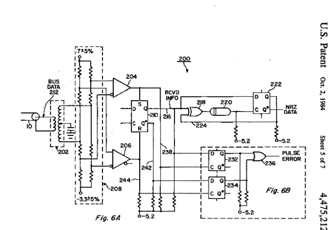
An enable/inhibit signal may be provided via line 176 of line receiver 206 via line 244. Consequently, the Q to both of line drivers 172 and 174, to disable the line output of flip-flop 234 indicates missing pulses. drivers and· prevent spurious signals from being placed The outputs of flip-flops 232 and 234 are combined by on the cable when data is not being transmitted. OR gate 236 to signal a pulse error when either flip-flop FIGS. 6A and 6B illustrate an exemplary recei- 5 detects an error. Basically, the circuit in FIG. 6B indi-ver/decoder circuit compatible with the encoder/trans- cates an error whenever it detects that the polarity of a mitter of FIG. 3. The basic receiver/decoder is shown oonsecutive pair of the received pulses has not alter-in FIG. 6A; FIG. 6B illustrates additional optional cir- nated.
cuitry which can detect pulse errors-i.e., the injection The same basic technique can be utilized, of course, of a spurious pulse (e.g., by noise) or the absence of a 10 for optical communications as well. In that situation, pulse which should have lieen present. however, d.c. isolation between drive and controller is Referring now specifically to FIG. 6A, the operation inherent in the use of an optical channel. Therefore, it is of the basic receiver/decoder circuit 200 will be ex- IlInnecessary to use the d.c. cancelling features of the plained. For this purpose, reference also will be made to c~e. One could, ror example, transmit over the cable a FIG. 7 which contains waveforms which may be ob- IS Signal correspondmg to what has been referred to above served 'at various points in the circuit of FIG. 6A. as the RCVD
IN~O
signal. Or a"~.c."
biascoul~
be Cable 10 is terminated at receiver/decoder 200 by the ~dded~ as shown m FIG. 8. That IS, a constant. hght primary winding of a pulse transformer 202. The sec- !ntenslty level 262 c~uld be used ~. a reference, WIth an ondary winding of transformer 202 is connected to a mcrease correspond~ng to a poslt~ve pulse 264 and a pair of line receivers 204 and ~, through a resistive 20 de~re~ correspondmg to a negatlv~ pulse ~, asex-t network (indicated generally at 208). Resistive network plamed!n the Summary of the Inventlo~ sectlOn,.~bove.
208 provides. a matching impedance to terminate the ~at IS, the p~lsc:s need be only ~~latlv.el~,posltlve or cable and sets thresholds for the line receivers. Line relatIvely negatlv~, an.d the word rel8;t1ve should be
. . . I h I h·l understood to be Imphed above precedmg occurrences
receIver 204 detects posItIve pu ses on t ecab e, w I e 21. f" ·t· " d " t · " . te
r
.
06 d . I Th f oJ 0 POSI Ive an nega Ive , as appropna .me ~ecelver ~ et~cts negatlve'pu ses. e ou~pu~ 0 Moreover, while relatively positive and negative receIver 204 IS supphe~ to the ~et mput. (S) of ~ fllp- op electrical or optical pulses are shown or discussed ex-210, a~d the output ofhne rec:lver 206 IS supphed to !he plicitly, they are used only as examples. In general, all reset mput (~~ of the same flIp-flop. Th~s, the leadmg that is required is the use of two different types of sig-edge of~ posItIve pulse on ~able 10 sets flIp-flop 210 a~d 30 nals of known duration, and· that is all the word "pulses" the leadmg. edge o~ a negatIve pulse on cable 10 resets ~t. is intended to indicate.
By way o~ Illustratl?n, for the bus data waveform 212m Having thus described exemplary embodiments of the FIG: 7, thIS results m .the wavef~~ 214 at the Q output invention, it will be apparent that various alterations, of flIp-flop 210,. on hne 216; thIS IS referred to as the modifications and improvements will readily occur to RCVD INFO sIgnal. 35 those skilled in the art. Such obvious alterations
modifi-The Q o~tput of flip-flop 210 !s supplied to ~ NRZ cations and improvements, though not expr~ly de-reconstructIon n.etwork compnsed .o.f exclUSIve-OR scribed above, are nonetheless intended to be implied gate 2~8, del~y h~e 220 a~d D-type flIp-flop 2~2. For and are within the spirit and scope of the invention.
~ecodmg the I'h bIt, excluslve-O~ gate 218 r~cel~es, on Accordingly, the foregoing discussion is intended to be
hne ~16, the wav~form of the I'h ~ell, whIch IS also 40 illustrative only, and not limiting; the invention is lim-supphed to the D mput of D-type flIp-flop 222. The Q ited and defined only by the following claims and equiv-output of flip-flop 222, representing the value of the alents thereto.
(i-I)lhbit is supplied as the other input to exclusive-OR What is claimed is:
gate 218 via line 224. The resulting output of the exclu- 1. A frequency-independent, self-clocking method for sive-OR gate is shown as waveform 226 in FIG. 7. The 45 communicating a stream of digital information bits from output of the exclusive-OR gate 218 is the input toa a sending device to a receiving device, the information delay line 220 which provides the same delay as delay bits being communicated at a data rate, wherein each bit lines 128 and 138. The output of delay line 220, shown is provided for an interval termed a "bit cell" (Ti), the as waveform 228 in FIG. 7, strobes or clocks flip-flop beginnillg of each bit cell being termed its leading edge, 222, so that flip-flop 222 samples the RCVD INFO 50 such method comprising the steps of:
signal during the first pulse of each bit cell; the exclu- (a) at the leading edge of the i'h bit cell (Ti), transmit-sive-OR gate prevents flip-flop 222 from responding to ting a pulse of a first type when the
i
,h bit is a 1 andany subsequent pulses in the bit cell. The Q. output of transmitting a pulse of a second type when the
i
,hflip-flop 222 supplies the fully decoded NRZ data indi- bit is a 0, the pulses of the first and second type cated in FIG. 7 at waveform 230. 55 being of the predetermined, fixed duration;
By the addition of the simple circuit shown in FIG. (b) comparing the
i
,h bit with the (i+ 1)lh bit; and 6B, a single missing or added pulse can be detected. The (c) transmitting a second pulse during the i'h bit cell, circuit comprises a pair ofD-type flip-flops 232 and 234, after the first pulse has been transmitted in the i,hbit and an OR gate 236. Flip-flop 232 detects added pulses, cell, the second pulse being transmitted within a while flip-flop 234 detects missing pulses. The D input 60 predetermined time interval after the leading edge of flip-flop 232 is connected to line 216; which carries of the i'h bit cell, the time interval being fixed and the RCVD INFO signal, and the clock for that flip-flop being independent ofthe data rate, the transmission is provided by the output of line receiver Z04 on line of a second pulse being responsive to the compari-238. If the Q output of the flip-flop is a 1, an error is sion step indicating that the (i+ 1)lh bit has the sameindicated. 6S value as the i'h bit, the second pulse being of the
Similarly, the D input of flip-flop 234 receives the second type if the i'h bit is a I and being the first RCVD INFO· signal from the Q. output of flip-flop type if the ilhbit is a 0, whereby there is provided an 210, on line 242. Flip-flop 234 is clocked by the output encoded bit stream in which clock and data are
..
,
9
4,475,212
10
combined and which can be decoded without the leading edge of the
i
th bit having a logical "0"knowledge of the frequency or data rate of the bit value;
stream. (b) the first and second types of pulses having the
2. The method of claim 1 wherein the first type of same fixed, pre-determined duration such duration pulse has a first type of electrical polarity and the sec- 5 being no greater than half the duration of a bit cell ond type of pulse has opposite electrical polarity. and being independent of the data rate;
3. The method of claim 1 wherein the first type of (c) means (108) for comparing the value of the ith bit
pulse comprises an optical signal (264) differing in am- with the value of the (i+ l)th bit;
plitude in a first direction from an average level (262) (d) means (104,106) responsive to the means for com-and the second type o( pulse comprises an optical signal 10 paring, for generating a second pulse during the bit (266) differing in amplitude in the opposite direction cell, after the pulse at the leading edge of the cell, from the average level (262). responsive to the (i+ l)th bit having the same value
4. The method of any of claims 1-3 wherein the dura- as the ith bit;
tion of each bit cell is at least as long as the combined (e) said second pulse being of the second type if the duration of two pulses, one of the first type and one of IS leading edge pulse was of the first type and being of
the second type. the first type if the leading edge pulse was of the
5. The method of any or"claims 1-3 wherein pulses of second type; and
the first and second types have equal, but opposite, (1) means for combining said leading edge pulses and average amplitude values, whereby the average value said second pulses into a unified pulse train, to of the encoded signal is substantially constant, to facili- 20 provide an encoded signal.
tate a.c. coupling of the encoded signal between the 9. The apparatus of claim 8 wherein the first type of sending device and the receiving device. pulse is a constant amplitude pulse of a first electrical
6. A method for communicating binary digital infor- . polarity and the second type of pulse is a constant am-mation ftom a sending device to a receiving device at a plitude pulse whose amplitude is equal in magnitude but data rate, wherein each bit to be communicated is avail- 25 opposite in polarity,
able for an interval termed a "bit cell", the beginning of whereby the encoded signal produced thereby has a each bit cell being referred to as its leading edge, such constant average value, facilitating the a.c. cou-method comprising, at the sending device, the steps of: pling of such signal between a sending device and
(a) at the leading edge of the ith bit cell, transmitting a receiving device.
a signal of a first type when the ith bit is a 1 and 30 10. Apparatus for decoding a signal representing an
transmitting a signal of a second type when the ith encoded binary digital data signal and a clocking signal
bit is a 0; therefor, to provide a decoded NRZ signal
correspond-(b) comparing the ith bit with the (i + l)th; and ingto said binary data signal, wherein for each bit ofthe (c) a predetermined, fixed duration after the leading binary data signal there is a corresponding interval edge of the bit cell, changing the transmitted signal 35 termed a "bit cell", the beginning of each bit cell being from the first type of signal to the second type or termed its "leading edge", and the encoded signal in-vice-versa, responsive to the comparison step indi- cludes, for each bit cell; a first pulse at the leading edge cating that the (i+ l)th bit has the same value as the of the bit cell indicating the value of the data bit associ-ith bit, and not changing the type of signal transmit- ated therewith and, when the bit value of the data bit in
ted responsive to the comparison step indicating 40 th~.next succeeding bit cell is the same as the bit value that the (i+ l)th bit and the ith bits have different for said cell, a second pulse opposite in polarity relative
values, said fixed duration being independent of the to said first pulse, said decoding apparatus including
data rate. means for discriminating between said first pulses and
7. The method of claim 6 further including, at the said second pulses; and means (200) responsive to said receiving device, the steps of: 4S means for discriminating, for determining the value of
responsive to the transmitted signal, generating a each of said first pulses and for holding each of said received information (RCVD INFO) signal which determined values between successive ones of said first assumes a first state responsive to reception of a pulses, the held values being the decoded NRZ signal; signal of said first type and assumes a second state said means for discriminating including a delay of a responsive to reception of a signal of said second SO duration which is fixed and independent of the rate at
type; which the data bits occur.
sampling the received information signal during the 11. Apparatus for decoding a digital signal to provide first or second type signal transmitted at the lead- a decoded NRZ signal, the encoded signal being a ing edge of each bit cell stream of relatively positive and relatively negative holding the logical value of the sample unchanged 55 pulses of predetermined, fixed duration, the stream in-between successive samples (272), cluding data pulses and compensation pulses, the decod-whereby such sample corresponds to the NRZ wave- ing apparatus comprising:
form provided to the sending device. (a) means for detecting said negative pulses; 8. Apparatus for encodmg an NRZ binary digital (b) means for detecting said positive pulses;
signal for communication at a data rate from a sending 60 (c) means responsive to the negative and positive device to a receiving device, each bit of said signal pulse detecting means for setting a bilevel signal to being present for an interval termed a "bit cell" and the a first binary level at the leading edge of a negative beginning of each bit cell t>eing termed its leading edge, pulse and for setting said bilevel signal to a second
comprising: . binary level at the leading edge of a positive pulse;
(a) means (102, 106, 108, 100, 112) for generating a 65 and
first type of pulse at the leading edge of the ith bit (d) means for sampling said bilevel signal at a
prede-cell responsive to the ith bit having a logical "I" termined time after the leading edge of a pulse,
value and for generating a second type of pulse at such predetermined time being fixed and
indepen-' " ' I ,.
11
4,475,212
dent of the rate at which the data pulses occur in the stream and for holding the sampled values thereof between the taking of samples, such that the sampled values constitute the decoded NRZsignal. 5
12. Apparatus for decoding a digital signal which has been encoded into a stream of relatively positive and relatively negative pulses of predetermined, fixed d1ilJia-tion, to provide a decoded NRZ signal comprising:
(a) means 206 for detecting said negative pulses; (b) means 204 for detecting said positive pulses;
10
(c) flip-flop means 210 responsive to the negative and positive pulse detecting means for setting a bistable signal to a first binary level at the leading edge of a 15
negative pulse and for setting said bistable signal to a second binary level at the leading edge of a posi-tive pulse;
(d) means 222 for storing a sample of the bistable signal from one sample time to a next sample time, 20
responsive to a clocking signal, said stored bistable signal comprising the logical complement of the decoded NRZ signal;
25
30
35
'~., "'. <-.I,.
40
45
.50.
55
60
65
( J " ,
12
(e) means for generating a clocking signal, compris-ing
(1) an exclusive-OR gate 218 receiving as a first input the bistable signal and as a second input the stored bistable signal; . (2) delay means 222 connecting the output of the
exclusive-OR gate to the means for storing a sample of the bistable signal for providing, as a clocking signal, the output of the exclusive-OR gate delayed by an interval equal to the predeter-mined pulse duration.
13. The apparatus of claim 12 further including means responsive to the positive and negative pulse detecting means for sensing the occurrence of two successive pulses of the same polarity without an intervening pulse of opposite polarity.
14. The apparatus of claim 8 wherein the first type of pulse comprises an optical signal (264) differing in am-plitude in a first direction from an average level (262) and the second type of pulse comprises an optical signal (266) differing in amplitude in the opposite direction from the average level (262).