Built-In-Self-Test of Analogue Circuits Using Optimised Fault Sets and Transient
Response Testing
N. Axelos, J. Watson, D. Taylor, A. Platts
Dept. Electronic and Electrical Eng.
University of Huddersfield
Queensgate
Huddersfield
HD1 3DH
England
[email protected]
Tel: UK (44) 1484 472468/472304
Fax: UK (44) 1484 472252
Abstract
Transient Response Testing has been shown to be a very powerful and economical functional test technique for linear analogue cells in mixed-signal systems. Recently this work has been extended to non-linear analogue circuits by treating Transient Response Testing as a structural test technique and employing optimised and reduced fault sets that are derived from Inductive Fault Analysis and circuit sensitivity analyses. These developments have been very successful and have also facilitated a novel BIST methodology for analogue circuits. The BIST scheme employs a generic on-chip stimulus for all analogue cells and features a specially designed test cell that coordinates a short test sequence that involves sampling the transient response at key instants in the test cycle and comparing to a known reference.
1. Introduction
Production testing of analogue cells in today’s mixed-signal systems is a very time consuming and expensive business. This has stimulated a lot of interest in new test techniques that are aimed at reducing test time. One such technique is Transient Response Testing (TRT).
Almost a decade of research has shown TRT to be a powerful functional test technique for linear analogue cells in mixed-signal systems [1-5]. The basic concept of a TRT is to inject a square, logical-amplitude stimulus into the circuit under test and to monitor the resulting impulse response. The advantages of TRT are that:
1. The logic amplitude stimuli employed can be injected into and propagated around mixed-signal systems
with ease, either via primary inputs, existing digital circuitry or the Boundary Scan Path.
2. By controlling the pulse width, so that its frequency content matches the full bandwidth of the circuit under test, TRT can be considered to perform a rapid pseudo-exhaustive functional test.
3. Test program generation is trivial, test execution time can be cut dramatically and a mixed-signal test routine can be run using only a conventional digital tester with an analogue data capture channel.
The observed response of the cell is usually compared with a “golden response” by using a correlation-based metric in order to determine if the component is faulty or fault-free [2].
In order to provide test access to buried analogue cells a digital scan path-based test strategy is used to isolate the CUT by the use of an Interface Scan (IS) as defined in the standard for Boundary Scan [6].
When the analogue cell is buried deep within the substrate then an additional form of access is required. One solution is to use sampling and quantisation [3] and then to scan the digital results out via the interface scan path. Another solution is to monitor the dynamic current consumption of the IC by using a built-in current sensor that maps disturbances in the device supply current to the response of the circuit under test [4].
For linear cells TRT can be considered to be a pseudo-exhaustive functional test, as the essential functions of a component are defined by its frequency response. However, for non-linear cells this is not the case and one would initially surmise that a TRT of such components would be a fundamentally flawed concept.
techniques employed in this extension to non-linear circuits have led to a powerful new BIST technique.
2. Transient Response Testing as a Structural
Test
For the purpose of this BIST study we present results from a Sample and Hold circuit.
[image:2.612.63.294.182.373.2]2. 1 The Sample and Hold Circuit
Figure 1: Sample and Hold Circuit
Parameter Conditions Min Typ Max Units Bandwidth 10mV AC 4V DC off-set 6.57 6.62 7.66 MHz
Slew Rate + sample mode, 0V to 8V step CL=10pF measured in
from 20% to 80% 34 43.6 52.2 V/ms
Slew Rate - sample mode, 8V to 0V step CL=10pF measured in
from 20% to 80% 138.7 149.1 158.4 V/ms Input Range Off set 4VDC 200KHz signal 0 - 8 V Input Impedance This was taken at the BW 1.5 1.55 1.6 KW Output Impedance This was taken at the BW 525 547 573 W
Hold Step Vin=4V 131 132 133 mV
[image:2.612.319.547.320.718.2]PSRR+ Vin=4V 8.8V<=VDD<=11.2V 259.7 259.8 262.5 dB PSRR- Vin=4V -1.2<=VSS<=1.2V 138.1 138.8 139.4 dB Supply Current Vin=4 0.843 0.846 0.85 mA Acquisition Time 0V to 8V step to 0.1% 136 160 203 ns Acquisition Time 0V to 8V step to 0.01% 394 460 590 ns
Table 1: Specification for the Sample and Hold Circuit
Typical values:
SR+ gives a Max input frequency over the 4V amplitude of 1.73MHz.
Taking the Acquisition Time the to 0.1% the max input frequency is 3.125MHz.
Taking the Acquisition Time to 0.01% the max input frequency is 1.086MHz.
Taking the sampling ACQ1 Fclk max 6.25MHz and for ACQ2 Fclk max 2.172MHz.
Minimum values:
SR+ gives a Max input frequency over the 4V amplitude of 1.35MHz.
Taking the Acquisition Time the to 0.1% the max input frequency is 3.676MHz.
Taking the Acquisition Time to 0.01% the max input frequency is 1.269MHz.
Taking the sampling theory ACQ1 Fclk max 7.352MHz and for ACQ2 Fclk max 2.538MHz.
Maximum values:
SR+ gives a Max input frequency over the 4V amplitude of 2.077MHz.
Taking the Acquisition Time the to 0.1% the max input frequency is 2.463MHz.
Taking the Acquisition Time to 0.01% the max input frequency is 0.847MHz.
Taking the sampling theory ACQ1 Fclk max 4.926MHz and for ACQ2 Fclk max 1.694MHz.
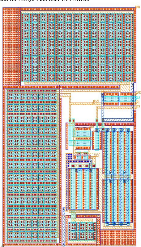
Figure 2: Floorplan of the Sample and Hold Circuit
Vout Vin
CLK
[image:2.612.57.294.396.615.2]2.2 Test Set-up, Fault Modelling , Fault Set Reduction and Response Analysis
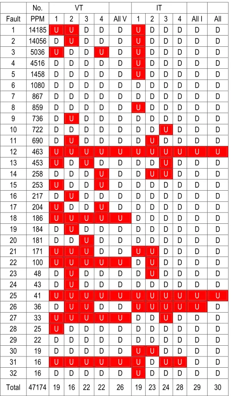
Previously published studies using Inductive Fault Analysis (IFA) in order to predict the most likely faults in analogue circuits have generally deduced that short circuits are by far more common than open circuits [7,8]. We have similarly derived a reduced fault set by producing a typical circuit layout, shown in Figure 2, then running IFA (VLASIC [9]) using some process defect statistics provided by an industrial partner. The IFA of the Sample and Hold circuit produced a graded fault list of 32 faults.
No. VT IT
Fault PPM 1 2 3 4 All V 1 2 3 4 All I All 1 14185 U U D D D U D D D D D 2 14056 D U D D D U D D D D D 3 5036 U D D U D U D D D D D
4 4516 D D D D D U D D D D D
5 1458 D D D D D U D D D D D
6 1080 D D D D D D D D D D D 7 867 D D D D D D D D D D D
8 859 D D D D D U D D D D D
9 736 D U D D D D D D D D D
10 722 D D D D D D D U D D D
11 690 D U D D D D U D D D D
12 463 U U U U U U U U U U U
13 453 U D U D D D D U D D D
14 258 D D D U D D U U D D D
15 253 U D D U D D D D D D D
16 217 D U D D D D D D D D D
17 204 U D D U D D D D D D D
18 186 U U U U U D D D D D D
19 184 D U D D D D D D D D D
20 181 D D U D D D D D D D D
21 171 U U U D D U U D D D D 22 100 U U U U U D U D D D D
23 48 D U D D D D U D D D D
24 43 D U D D D D D D D D D
25 41 U U U U U U U U U U U
26 36 D U U D D U U U U U D
27 33 U U U U U D D U D D D
28 25 U D D D D D D D D D D
29 22 D D D D D D D D D D D
30 19 D D D D D U U D D D D
31 16 U U U U U U D U U D D
32 16 D D D D D U D D D D D
[image:3.612.60.297.232.638.2]Total 47174 19 16 22 22 26 19 23 24 28 29 30
Table 2: IFA and Fault Detection Sample and Hold Circuit
The Sample and Hold circuit was tested by applying a 100ns pulse to the input whilst the circuit was in “sample” mode, resulting in a bandwidth-limited pulse response and the results are shown in Table 2, then summarised in Table 3.
There are a number of other factors to consider for a BIST scheme. Firstly we would not want to capture and compare an entire response in order to detect faults. We have therefore looked at four arbitrary points in the test response at T1, T2, T3 and T4 and sampled both voltage and supply current. In order to define a fault detection we ran a Monte Carlo simulation of the fault-free circuit using industrial parameters and specified that for a fault to be classified as detectable, it must result in a response that is outside of the normal fault-free Monte Carlo spread. An open circuit was modelled using 100MΩ in parallel with a 1fF capacitor, since HSPICE does not permit floating nodes, and a short circuit by a 1Ω resistor [7,8]. Secondly we want to detect as many of the faults as possible, but need to quantify fault coverage in the light of the IFA results.
Unfortunately, there are two faults which are not detected by this simple test, but they are low down in the list and account for only about 500 PPM of test escapes. The voltage samples can detect 26 of the 32 faults and miss approximately 850 PPM test escape whilst the current samples can detect only 28 of the 32 faults and miss approximately 550 PPM test escapes. Interestingly IT4 can detect all but about 550 PPM of test escapes on its own.
Of course all of the data which has been derived in this way is process and layout dependent and will provide different results for different circuits, but nevertheless serves to illustrate the potential benefits of this technique.
Test Detection’s Fault Undetected escapes PPM
VT1 19 13 21166
VT2 16 16 31205
VT3 22 10 1680
VT4 22 10 6590
VT3+VT4 26 6 839
All V 26 6 839
IT1 19 13 40872
IT2 23 9 1826
IT3 24 8 2022
IT4 28 4 556
All I 29 3 540
[image:3.612.320.551.416.554.2]All VT’s & IT’s 30 2 504
Table 3: Fault Detection’s for the VCO Voltage and Current Tests
3. BIST
With these reduced fault sets it has been shown that we can often detect all faults, or a very large percentage of them, by employing a transient response test and sampling the output response (voltage or current) just once or twice, then comparing the resulting sample with a known reference. Consequently, we can implement a relatively simple, but powerful, BIST scheme.
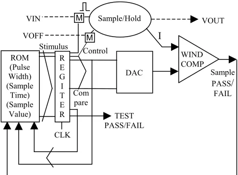
The developed BIST cell generates a pulse of a given width, then samples and compares the circuit response with the fault-free response, at one or more points in time after the start of the test. A single micro-coded finite state machine, a DAC and a comparator coordinates a BIST scheme for all analogue cells on the chip as shown in Figure 3.
[image:4.612.60.293.419.591.2]The ROM stores code words that contain information on pulse width, the times to sample the test response and the expected sample. Whilst continually cycling through its microcode the state machine first takes control of the CUT via the input multiplexors then generates a test pulse of the required duration. When it is time to sample the test response it generates a binary compare code that is transformed into an analogue signal by the DAC and used by the window comparator to gauge the actual response from the circuit. The resulting sample pass/fail signal is then fed back to the state machine and used, in conjunction with any further samples, to generate an overall pass/fail signal for the whole test sequence.
Figure 3: TRT and BIST of the Sample and Hold Circuit
This test cell has only been modelled behaviourally at this stage and in this case we chose to sample only the current at I4 after 750ns, with which we can detect all but about 550 PPM of test escapes. To sample the current we use the techniques described in [4] and to determine the necessary accuracy of the comparison we use the Monte Carlo simulation of the fault-free circuit and the techniques described in [3].
Of course an ASIC needs only one such structure, which can be optimised and built into the background architecture.
4. Conclusions
Transient Response Testing has always been thought to be a powerful functional test technique, but its use as a structural test technique has also been shown to facilitate a generic BIST scheme for analogue circuits.
By using IFA and circuit sensitivity analysis to reduce and grade the fault set it has been shown that we can detect most of the important faults by taking a small number of response samples and comparing, on-chip, to an expected response.
The next stage of this research will involve the development of techniques for optimising both the test cell and the sample points, looking at larger hierarchical circuits and more complex test scenarios.
Acknowledgement
This work was supported by the EPSRC under grant GR/M33266 and is ongoing under grant GR/R46281.
5. References
1. P. S. A. Evans, M. Al Qutayri, P. R. Shepherd, “A Novel Technique for Testing Mixed-Signal ICs”,Proceedings of ITC, 1991, pp301-306
2. D. Taylor, and P.S.A.Evans, and T.I.Pritchard: ‘Testing of Mixed-Signal Systems Using Dynamic Stimuli’, Electron. Letters, 1993, 29, (9), pp811-813
M Sample/Hold
VIN VOUT
I
VOFF M
Stimulus Control
WIND
COMP 3. I. C. Butler, D.Taylor, and T.I.Pritchard: ‘Effects of Response Quantisation on the Accuracy of Transient Response Test
Results’, IEE Proceedings Circuits Devices Systems., 1995, 142, (5), pp 334-338
ROM (Pulse Width) (Sample Time) (Sample Value) R E G I T E R Sample PASS/ FAIL DAC Com pare
4. R. J. Binns, D. Taylor, T. I. Pritchard, "Testing Linear Macros in Mixed-Signal Systems using Transient Response Testing and Dynamic Supply Current Monitoring" IEE Electronics Letters, No.30, Vol. 15 , 21st July 1994, pp 1216-1217
TEST PASS/FAIL CLK
5. R. J. Binns, D. Taylor, T. I. Pritchard, “Generating, Capturing and Processing Supply Current Signatures from Analogue Macros in Mixed-Signal Systems”, The Microlectronics Journal, Vol. 27, 1996.
6. IEEE Standard 1149.1: “Standard Test Access Port and Boundary Scan Architecture”, The Computer Society, IEEE, 1990
7. M. Sachdev, “A defect oriented testability methodology for analog circuits,” Journal of Electronic Testing: Theory and Applications, vol. 6, no. 3, 1995, pp. 265-276.
9. H. Walker and S.W. Director, “VLASIC, A catastrophic fault yield simulator for integrated circuits,” IEEE Transactions on Computer Aided Design of Integrated Circuits and Systems, Vol. CAD-5(4), 1986, pp. 541-556.
10. A. Milne, D. Taylor, K. Naylor, “Assessing and Comparing Fault Coverage When Testing Analogue Circuits”, IEE Proceedings Circuits Devices and Systems, Vol. 144, No. 1, 1997, pp1-4.