N A N O E X P R E S S
Open Access
Design and adjustment of the graphene
work function via size, modification,
defects, and doping: a first-principle theory
study
Ning Yang
1, Daoguo Yang
1*, Liangbiao Chen
2, Dongjing Liu
1, Miao Cai
1and Xuejun Fan
2Abstract
In this work, the work function (WF) of graphenes, which are used as electronic devices, has been designed and evaluated by using the first-principle approach. Different states of graphene were considered, such as surface modification, doping, and defects. Firstly, WF strongly depends on the width of pristine graphene. A bigger width leads to a smaller WF. In addition, the effects of hydroxyls, defects, and positions of hydroxyls and defects are of concern. The WF of the graphene which is modified with hydroxyls is bigger than that of the pristine graphene. Moreover, the WF value increases with the number of hydroxyls. Positions of the hydroxyls and defects that deviated from the center have limited influence on the WF, whereas the effect of the position in the center is substantial. Lastly, B, N, Al, Si, and P are chosen as the doping elements. The n-type graphene doped with N and P atoms results in a huge decline in the WF, whereas the p-type graphene doped with B and Al atoms causes a great increase in the WF. However, the doping of Al in graphene is difficult, whereas the doping of B and N is easier. These discoveries will provide heavy support for the production of graphene-based devices.
Keywords:Work function, Graphene, Functional groups, Defects, Positions, Doping, First-principle theory
Background
As a material that possesses a variety of excellent perfor-mances, graphene [1–3] has been widely used in different areas, such as sensors, field-effect transistors (FET), elec-trode of photovoltaic devices, Schottky diodes, vacuum tube, and metal–semiconductor junction of light-emitting diodes, and has become a substitute for many materials [4–7]. Graphenes can solve miniaturization problems of FET and the cost of photovoltaic devices while maintain-ing good stability and electrical performance. However, graphene work function (WF) has a crucial influence on the performance of these electronic devices. Therefore, knowing and controlling the WF of graphenes is of great significance to graphene-based electronic devices. Gener-ally, the performance of FET devices can be determined by the WF of source/drain electrodes [8–10]. With the
differences in WF of materials after the metal– semicon-ductor contact, a potential difference will exist in the interface, which has a direct effect on Schottky or ohmic contact [10]. Given that the band alignment of two differ-ent materials is determined by their respective WFs, con-trolling the graphene WF is the key in reducing the contact barriers [11].
Graphene WF measured via experiment is approxi-mately at 4.2 to 4.8 eV [12, 13]. The change of Fermi level will lead to the change of WF. Many experiments and the-oretical analysis showed that the Fermi level of graphenes can be adjusted through deliberate doping by aromatic and gas molecules [14, 15] or ultraviolet irradiation [16], surface functionalization [17, 18], defects [19], and elec-trostatic gating [20]. For example, Yuan et al. found that the WFs of graphene change dramatically via the adsorption of Na and Cl [21]. Zhang et al. showed that the WF can be finely tuned within the range of 4.0–4.5 eV by covering the graphene with alkali metal cations [22]. Leenaerts et al. learned the graphene * Correspondence:[email protected]
1The Faculty of Mechanical and Electrical Engineering, Guilin University of Electronic Technology, Guilin 541004, China
Full list of author information is available at the end of the article
intrinsic characteristics. The results showed that the WF of fewlayer graphene was almost independent of the number of layers, but it can be modulated by dipole layer [23]. Volodin et al. and Peng et al. used the mechanical method to change the graphene WF [24]. All of them found that the WF will increase with the strain. Yu et al. used electric field effects to adjust the WF of graphene and demonstrated that the WF can be tuned within the range 4.5–4.8 eV for monolayer graphenes and 4.65–4.75 eV for bilayer graphenes in ambient and dry ni-trogen conditions [25]. Shi et al. found that the surface po-tential of graphene films can be adjusted by controlling the immersion time. For doping time less than 20 s, the surface potential was monotonically increased to about 0.5 V [13]. Moreover, irradiation was found to be an efficient method in controlling the doping concentration. Stratakis et al. controlled the doping and reaction levels to tailor the WF of the GO–Cl layers from 4.9 eV to a maximum value of 5.23 eV by tuning the laser exposure time [26]. However, Kang et al. tuned the WF of graphene oxide via direct sur-face functionalization [27].
Although many previous studies have reported methods to control graphene WF, the research results are not com-prehensive enough. For example, the comparative study about the size effect of different chiral graphene on WF does not provide sufficient information. Additionally, the effects of graphene’s modifications and defects on WF are still not very clear. Although the effect of doping on gra-phene WF was studied, the corresponding formation en-ergy of doping atoms was not mentioned. For example, in Shi’s experiment, the graphene was immersed in an AuCl3
solution to adjust the WF [13]; however, the relationship between WF and doping concentration was still unclear. In addition, it has to be noted that the impacts of the posi-tions of functional groups and defects on graphene WF have not yet been reported. Given the expensive cost of WF’s controlling methods, intrinsic characteristics of the different methods must be investigated.
In this paper, a comprehensive study on the controlling methods of the WF was investigated via the first-principle theory. Effects of the doping and the positions of hydroxyls and defects were first reported and highlighted. First, gra-phenes with different chirality (zigzag and armchair) were considered, and the dependence of WF on the graphene width investigated. Second, the WFs of the graphene with surface modifications and defects were calculated. Different distributions of hydroxyls were first compared, followed by the effect of defects at various positions. Third, B, N, Al, Si, and P were chosen as the doping elements to study the doping effect of WFs.
Methods
All calculations were performed in CASTEP code based on the density functional theory (DFT) [28], which is a
kind of quantum mechanics research for the electronic structure of the multi-electron system. DFT has been widely used in the study of physical and chemical proper-ties, including nanomaterials of graphenes and carbon nanotubes [29, 30]. DFT can also accurately simulate tens to hundreds of atomic systems and describe the atom as quantum particles, namely, the set of nuclei and electrons [31].
The generalized gradient approximation (GGA) and local density approximation (LDA) are the exchange– correlation functionals commonly used in quantum mechanics calculations. They are described in Eqs. (1) and (2):
Exc½ ¼ρ
Z
fxc½ρð Þr ;jΔρð Þ jr dr ð1Þ
Exc½ ¼ρ
Z
drρð Þr εxc½ρð Þr ð2Þ
where RI and r are the coordinates of the atomic nu-cleus and the electron, respectively. The exchange– cor-relation energy in inhomogeneous electron gas is replaced by the Exc[ρ] in uniform electron gas. Both
GGA and LDA have been used for the calculations in two-dimensional materials. Lebègue et al. found that the band structure of two-dimensional materials obtained using either LDA or GGA is very similar [32]. At the same time, GGA was used in the calculation of the elec-tric properties of graphene in Kharche’s and Gui’s re-searches, which guarantees the accuracy [33,34].
Results and discussion
WF of zigzag and armchair graphenes with different sizes
Generally speaking, WF can be defined as the minimum energy needed to extract an electron from bulk to infin-ity [42]. As in quantum mechanics calculations, WF is defined as the difference between the vacuum level (V0)
and the Fermi level (Ef), as shown in Eq. (3):
WF¼V0−Ef ð3Þ
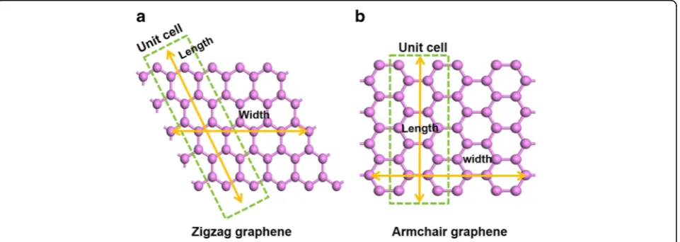
CASTEP calculations for crystal surfaces are carried out on slabs with a region of vacuum. Effectively, an in-finite array of 2D-periodic slabs of material is separated by wide vacuum spacings. CASTEP produces the Fermi energy for such systems and the spatial distribution of the electrostatic potential [43]. Graphene with different widths has various properties. The models with different chirality of zigzag and armchair were chosen to elucidate the effect of width on the WF. In this calculation, sam-ples with the range of one- to seven-unit cells were cal-culated. Figure 1 illustrates the definition of the size of zigzag and armchair graphenes. The crystal orientation of zigzag and armchair graphenes is different; the crystal structure of zigzag graphene is rhombic but the crystal structure of armchair graphene is dimetric, as shown in Fig. 1a, b. The width of the graphene is defined in the horizontal direction, and the length of the graphene is defined in the vertical direction. In addition, a unit cell is set as a carbon ring.
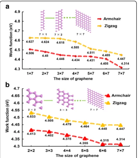
Graphene band gap changes with the change of gra-phene’s width. Generally speaking, the zigzag graphene presents a metallic property, and armchair graphene shows a half-metallic property. However, what is the re-lationship between WF and width in graphenes? Figure 2 shows the relationship between the graphene size and the WF. The length and width of graphenes are unequal
in Fig. 2a in which the length is constantly set as seven-unit cells but the width is arranged from one-seven-unit to seven-unit cells (1 × 7 to 7 × 7), whereas the length and width are equal in Fig. 2b in which the size is arranged from 2 × 2 supercells to 7 × 7 supercells. The WF is af-fected greatly by the graphene width. Generally, with the increase of graphene size, the WF decreases. Moreover, the WF of zigzag graphenes is always bigger than that of armchair graphenes. We suggest that this phenomenon is caused by the crystal structure of graphene. Actually, crystal orientation has a big impact on the materials’ performance. The crystal structure of zigzag graphene is a cube structure, while the crystal structure of armchair graphene is a diamond structure. By comparing the WF between Fig. 2a, b, the WF of the graphenes (the gra-phene in Fig. 2a) with the unequal width and length would be bigger than that of the graphene (the graphene in Fig. 2b) with the equal width and length. The reduc-tion gradient of the WF in Fig. 1a is also larger. Further-more, the WF difference between the 6 × 6 and 7 × 7 supercells in the armchair and zigzag graphenes is small; we believe that the WF will be stable when the graphene size is up to the 6 × 6 supercells.
The band gaps of graphenes with various widths were also analyzed, as listed in Table 1. In general, graphenes with a small size will have a small band gap. However, as the width increases, the band gap decreased or even closed [44]. Son et al. have shown that graphene nanor-ibbons with homogeneous armchair- or zigzag-shaped edges all have energy gaps which decrease as the widths of the system increase [45]. Table 1 also shows that the band gap decreased with the size of graphene. Overall, the band gap of armchair graphenes is smaller than that of zigzag graphenes. Graphenes with the unequal width and length also possess a bigger band gap than graphenes with the equal width and length.
[image:3.595.60.541.534.705.2]Effects of hydroxyls, defects, and positions of hydroxyls and defects on the WF
Functionalization is always taken as a modification method in designing and improving the performance of the target material; hydroxylation is one of these methods. The influence of quantity and the position of hydroxyls and defects on the WF are analyzed, as shown in Fig. 3. Insets (a) and (b) illustrate the structure diagrams of hydroxyl and defect positions in graphene, respectively. In this calculation, pristine zigzag gra-phenes with 4 × 4-supercell size is selected, and the cal-culated WF is 4.479 eV, which is slightly smaller than that of the experiment result [12]. The hydroxyl
modification will result in WF increase. Kang et al. determined the WF value of oxide graphene through ex-periment was 4.91 eV [27]. However, the number of the functional groups and their positions were not reported. The WF of zigzag graphenes with one hydroxyl we cal-culated is 4.504 eV, which is bigger than that of pristine zigzag graphenes. Along with the increase of the hy-droxyls, the WF increases. Moreover, the increment is relatively large; the maximum WF reaches 5.102 eV. This result is due to the hydroxyl effect, which is highlighted with the increasing number of the hydroxyls. In addition, four hydroxyls are chosen to analyze the ef-fect of the distribution of functional groups on the WF. Inset (a) gives four different ways hydroxyls can be dis-tributed; the distributions are symmetrical. With inten-sive distribution, the WF is large. However, with dispersed distribution, the WF is small. The maximum value of WF is 4.829 eV, whereas the minimum value of WF is 4.658 eV. This phenomenon should be caused by the aggregation effect of hydroxyls. In addition, four dif-ferent defect sites in the 4 × 4 graphene are investigated, as shown in inset (b). In general, the defects will result in the decrease of graphene WF. Bae et al. showed that the graphene WF was smaller when the vacancy existed. And the smaller the defect ratio was, the smaller the WF became [46]. The WF of graphene with the defect at the center is 4.337 eV, whereas the WF of graphene with the defect deviated from the center is larger at 4.363 eV, which is slightly smaller than that of the 4 × 4 pristine zigzag graphene. This difference means that the defects in the center have more impact on the structure, so the WF is at its smallest. Therefore, we suggest that the cen-tral defect sites have a large effect on the WF, whereas defects deviated from the center have a smaller effect. Kim et al. found that hole doping leads to a difference in
[image:4.595.57.293.87.358.2]Fig. 2The relationship between graphene size and WF. The relationship between graphene size and WF. The length and width of graphenes are different in (a), whereas the same in (b)
Table 1The band gap of zigzag and armchair graphenes in various widths
Graphene size
Band gap (eV) Graphene size
Band gap (eV)
Zigzag Armchair Zigzag Armchair
1 × 7 0.696 0.540 – – –
2 × 7 0.351 0.311 2 × 2 0.345 0.334
3 × 7 0.145 0.123 3 × 3 0.129 0.007
4 × 7 0.054 – 4 × 4 0.009 0.003
5 × 7 0.024 – 5 × 5 0.009 –
6 × 7 0.004 – 6 × 6 – –
7 × 7 – – 7 × 7 – –
[image:4.595.307.539.88.250.2] [image:4.595.57.291.606.731.2]the WF by as much as 400 meV, which is consistent with what we are computing [47].
Effect of the dopants of B, N, Al, Si, and P on the WF
Doping is an effective way to control the WF, band gap, and adsorption properties. Thus, the doping effects and concentrations are investigated in this study. Figure 4 shows the effect of different dopants on the WF; the gra-phene’s size is 4 × 4 supercells. Dopants from 1, 2, 3, 4, 5, and 6 atoms respond to the concentrations at 2.4, 4.9, 7.3, 9.8, 12.2, and 14.6%, respectively. The effect of dop-ants on the WF is significant and follows a certain trend. First, the WF of all the doped graphenes decreases as the concentration increases except for the B-doped gra-phene, which displays an opposite effect. Legesse et al. also found that the WF of the alkali metal-doped gra-phene decreases with the increase of the concentration [48]. Second, the increment of the WF in B- and Al-doped graphene is relatively bigger than that of the other graphenes. By comparing the WF value, p-type gra-phenes doped with B and Al have bigger WF, and the maximum value is up to 5.148 eV for B-doped graphene at a concentration of 14.6%. By contrast, the WF is much smaller in n-type graphenes doped with N and P; the minimum value is decreased to 3.23 eV at a concen-tration of 14.6% in P-doped graphene. Kwon et al. also showed that the p-dopants would increase graphene WF from 4.2 to 5.14 eV [49]. Kvashnin et al. also demon-strated the phenomena that B doping would cause WF increase, but N and P doping resulted in WF decreasing [19, 50]. In addition, the WF of Si-doped graphenes is relatively stable. This may be due to the fact that C and Si atoms are congeners. Therefore, we suggest that the p-type doping would lead to WF increasing; however, the amount is determined by the doping elements. The WF tends to be stable at the concentration of 14.6%. On
the other hand, n-type doping will make the WF decrease sharply.
Although the influence of dopants on the WF has been analyzed and has the vital significance for the gra-phene application, the feasibility of doping for various atoms is different. Thus, we calculate the formation en-ergy of different doping atoms in GNRs. The formation energy [51] is described as Eq. (4):
Eformation ¼EðGNRsþdÞþnEC−EðGNRsÞ−nEd ð4Þ
whereEformationis the formation energy,E(GNRs) is the
energy of pristine GNRs, E(GNRs + d) is the energy of
doped GNRs,dis the doping atom,nis the number, and EC and Ed are the chemical potentials determined for
carbon and doping atoms.
The formation energy can be used to evaluate whether the feasibility of using atoms for doping is good or not. The smaller the formation energy is, the easier the dop-ing becomes. Figure 5 shows that the graphene doped with Al has the largest but most unstable formation en-ergy; the increase of the Al atoms leads to the dramatic changes of the structure in the graphene with 4 × 4-cell size. By contrast, the formation energy of B and N is very small, but small changes are evident with the in-crease of the number of atoms. The atoms of Al, Si, and P have more fluctuations in formation energy compared to the atoms of B and N. This is because the formation energies of Al, Si, and P in graphene are large, which means that the Al-, Si- and P-doped graphenes are less stable, especially the Al-doped graphene has the most unstable structure. They are relatively hard to be doped in graphene. Overall, the Al doping in graphene is diffi-cult, whereas B and N doping are easier. The WF and formation energy of these dopants in graphene are recorded in Table 2.
Fig. 4The relationship between the WF and the number of doping atoms. The relationship between the WF and the number of doping atoms. Different types of dopants, e.g., Al, B, P, N, and Si, are doped in the graphene with the size of 4 × 4 cells
[image:5.595.59.292.530.684.2] [image:5.595.303.540.531.684.2]Conclusions
The WF of graphene in different states, such as surface modification, doping, and defects, are investigated in this study. Basically, the WF decreases as graphene width in-creases. For the hydroxyl modification, the WF is large when the number of hydroxyls increases. Furthermore, when the distribution of hydroxyls is intensive, the WF is also increased. The defect would decrease the gra-phene WF, which does not depend on the positions. The p-type doping with B and Al would lead the WF to in-crease; however, the increased amount is determined by the dopants. The n-type doping with N and P reduces WF greatly. These discoveries will provide a theoretical support in controlling graphene and further improving the design of graphene-based devices.
Acknowledgements
This work was co-supported by the National Natural Science Foundation of China (51303033, 61434001), the Guangxi Natural Science Foundation
(2014GXNSFCB118004), the Natural Science Foundation of Guangxi Province (2016GXNSFBA380109), the Guangxi Key Laboratory of Manufacturing System and Advanced Manufacturing Technology (16-380-12-001Z), the China Post-Doctoral Science Foundation (2014M550065), the Guangxi Universities Scientific Foundation (YB2014116), the Guilin Science and Technology Development Foundation (20140103-3), the Natural Science Foundation of Guangxi Province under Grant (2016GXNSFBA380109), the Guangxi Key Laboratory of Manufacturing System and Advanced Manufacturing Technology under Grant (16-380-12-001Z), the Innovation Planning Projects of GuangXi Graduate Student Education (C66YJA240001), and the Innovation Project of GUET Graduate Education (2016YJCXB04).
Authors’contributions
NY and DY conceived the project. NY, DL, and LC performed the simulations. With the help of MC and XF, NY wrote and completed the paper. All authors read and approved the final manuscript.
Competing interests
The authors declare that they have no competing interests.
Publisher’s Note
Springer Nature remains neutral with regard to jurisdictional claims in published maps and institutional affiliations.
Author details
1The Faculty of Mechanical and Electrical Engineering, Guilin University of Electronic Technology, Guilin 541004, China.2The Department of Mechanical Engineering, Lamar University, Beaumont 77706, USA.
Received: 16 October 2017 Accepted: 17 November 2017
References
1. Geim AK (2009) Graphene: status and prospects. Science 324:1530–1534 2. Huang X, Qi X, Boey F, Zhang H (2012) Graphene-based composites. Chem
Soc Rev 41:666–686
3. Novoselov KS, Fal V, Colombo L, Gellert P, Schwab M, Kim K (2012) A roadmap for graphene. Nature 490:192–200
4. Vicarelli L, Vitiello M, Coquillat D, Lombardo A, Ferrari A, Knap W, Polini M, Pellegrini V, Tredicucci A (2012) Graphene field-effect transistors as room-temperature terahertz detectors. Nat Mater 11:865–871 5. Li N, Oida S, Tulevski GS, Han SJ, Hannon JB, Sadana DK, Chen TC (2013)
Efficient and bright organic light-emitting diodes on single-layer graphene electrodes. Nat Commun 4:2294
6. Georgiou T, Jalil R, Belle BD, Britnell L, Gorbachev RV, Morozov SV, Kim YJ, Gholinia A, Haigh SJ, Makarovsky O (2013) Vertical field-effect transistor based on graphene-WS2 heterostructures for flexible and transparent electronics. Nat Nanotechnol 8:100–103
7. Zhou Y, Fuentes-Hernandez C, Shim J, Meyer J, Giordano AJ, Li H, Winget P, Papadopoulos T, Cheun H, Kim J (2012) A universal method to produce low–work function electrodes for organic electronics. Science 336:327–332 8. Braga D, Horowitz G (2009) High-performance organic field-effect
transistors. Adv Mater 21:1473–1486
9. Park YD, Lee HS, Choi YJ, Kwak D, Cho JH, Lee S, Cho K (2009) Solubility-induced ordered polythiophene precursors for high-performance organic thin-film transistors. Adv Funct Mater 19:1200–1206
10. MacLeod BA, Horwitz NE, Ratcliff EL, Jenkins JL, Armstrong NR, Giordano AJ, Hotchkiss PJ, Marder SR, Campbell CT, Ginger DS (2012) Built-in potential in conjugated polymer diodes with changing anode work function: interfacial states and deviation from the Schottky–Mott limit. J Phys Chem Lett 3: 1202–1207
11. Jiang J, Krauss TD, Brus LE (2000) Electrostatic force microscopy characterization of trioctylphosphine oxide self-assembled monolayers on graphite. J Phys Chem B 104:11936–11941
12. Yan R, Zhang Q, Li W, Calizo I, Shen T, Richter CA, Hight-Walker AR, Liang X, Seabaugh A, Jena D (2012) Determination of graphene work function and graphene-insulator-semiconductor band alignment by internal photoemission spectroscopy. Appl Phys Lett 101:022105
13. Shi Y, Kim KK, Reina A, Hofmann M, Li LJ, Kong J (2010) Work function engineering of graphene electrode via chemical doping. ACS Nano 4: 2689–2694
14. Dong X, Fu D, Fang W, Shi Y, Chen P, Li LJ (2009) Doping single-layer graphene with aromatic molecules. Small 5:1422–1426
15. Wehling T, Novoselov K, Morozov S, Vdovin E, Katsnelson M, Geim A, Lichtenstein A (2008) Molecular doping of graphene. Nano Lett 8:173–177 16. Lin YJ, Zeng JJ (2013) Tuning the work function of graphene by ultraviolet
irradiation. Appl Phys Lett 102:183120
17. Bointon TH, Jones GF, De Sanctis A, Hill-Pearce R, Craciun MF, Russo S, Large-area functionalized CVD graphene for work function matched transparent electrodes. Sci Rep-UK. 2015;5:srep16464
[image:6.595.56.539.100.210.2]18. Ji S, Min BK, Kim SK, Myung S, Kang M, Shin HS, Song W, Heo J, Lim J, An KS (2017) Work function engineering of graphene oxide via covalent functionalization for organic field-effect transistors. Appl Surf Sci 419:252–258
Table 2The WF and formation energy of the 4 × 4 graphene doped with the atoms of Al, B, P, N and Si, respectively
The number of doping atoms
WF (eV) Formation energy (eV)
Al B P N Si Al B P N Si
1 4.309 4.767 3.53 3.615 3.987 10.618 2.7 6.85 2.312 7.069
2 4.312 4.806 3.253 3.455 3.919 9.972 2.881 6.546 2.384 7.588
3 4.229 4.926 3.169 3.355 3.902 11.257 2.915 6.868 2.43 7.602
4 4.106 5.103 3.139 3.254 3.889 11.88 3.007 7.09 2.446 7.92
5 3.869 5.126 3.108 3.302 3.806 10.5 3.075 7.419 2.521 8.429
19. Kvashnin DG, Sorokin PB, Brüning J, Chernozatonskii LA (2013) The impact of edges and dopants on the work function of graphene nanostructures: the way to high electronic emission from pure carbon medium. Appl Phys Lett 102:183112
20. Padilha J, Fazzio A, da Silva AJ (2015) Van der waals heterostructure of phosphorene and graphene: tuning the schottky barrier and doping by electrostatic gating. Phys Rev Lett 114:066803
21. Yuan G, Song X, Mimura H (2017) Modulation of the work function of graphene by Na and Cl coadsorbed on opposite sides on graphene. J Vac Sci Technol B 35:02C104
22. Zhang L, Ding, Z, Tong T, Liu J Tuning the work functions of graphene quantum dot-modified electrodes for polymer solar cell applications. Nano 2017; 9:3524-3529
23. Leenaerts O, Partoens B, Peeters F, Volodin A, Van Haesendonck C (2016) The work function of few-layer graphene. J Phys Condens Mat 29:035003 24. Volodin A, Van Haesendonck C, Leenaerts O, Partoens B, Peeters F (2017) Stress dependence of the suspended graphene work function: vacuum Kelvin probe force microscopy and density functional theory. Appl Phys Lett 110:193101
25. Yu YJ, Zhao Y, Ryu S, Brus LE, Kim KS, Kim P (2009) Tuning the graphene work function by electric field effect. Nano Lett 9:3430–3434
26. Stratakis E, Savva K, Konios D, Petridis C, Kymakis E (2014) Improving the efficiency of organic photovoltaics by tuning the work function of graphene oxide hole transporting layers. Nano 6:6925–6931
27. Kang B, Lim S, Lee WH, Jo SB, Cho K (2013) Work-function-tuned reduced graphene oxide via direct surface functionalization as source/drain electrodes in bottom-contact organic transistors. Adv Mater 25:5856–5862 28. Delley B (1990) An all-electron numerical-method for solving the local
density functional for polyatomic-molecules. J Chem Phys 92:508–517 29. Lazzeri M, Attaccalite C, Wirtz L, Mauri F (2008) Impact of the
electron-electron correlation on phonon dispersion: failure of LDA and GGA DFT functionals in graphene and graphite. Phys Rev B 78:081406 30. Chen XP, Yang N, Jiang JK, Liang QH, Yang DG, Zhang GQ, Ren TL (2015)
Ab initio study of temperature, humidity and covalent functionalization induced band gap change of single-walled carbon nanotubes. IEEE Electr Device L 36:606–608
31. Hohenberg P, Kohn W (1964) Inhomogeneous electron gas. Phys Rev 136(3B):B864
32. Lebegue S, Eriksson O (2009) Electronic structure of two-dimensional crystals from ab initio theory. Phys Rev B 79:115409
33. Gui G, Li J, Zhong J (2008) Band structure engineering of graphene by strain: first-principles calculations. Phys Rev B 78:075435
34. Kharche N, Nayak SK (2011) Quasiparticle band gap engineering of graphene and graphone on hexagonal boron nitride substrate. Nano Lett 11:5274–5278
35. Takahashi T, Tokailin H, Sagawa T (1985) Angle-resolved ultraviolet photoelectron spectroscopy of the unoccupied band structure of graphite. Phys Rev B 32:8317
36. Datta SS, Strachan DR, Mele E, Johnson AC (2008) Surface potentials and layer charge distributions in few-layer graphene films. Nano Lett 9:7–11
37. Filleter T, Emtsev K, Seyller T, Bennewitz R (2008) Local work function measurements of epitaxial graphene. Appl Phys Lett 93:3117
38. Giovannetti G, Khomyakov P, Brocks G, Karpan VV, Van den Brink J, Kelly P (2008) Doping graphene with metal contacts. Phys Rev Lett 101:026803 39. Choi SM, Jhi SH, Son YW (2010) Effects of strain on electronic properties of
graphene. Phys Rev B 81:081407
40. Monkhorst HJ, Pack JD (1976) Special points for Brillouin-zone integrations. Phys Rev B 13:5188
41. Methfessel M, Paxton A (1989) High-precision sampling for Brillouin-zone integration in metals. Phys Rev B 40:3616
42. Pourtois G, Lauwers A, Kittl J, Pantisano L, Soree B, De Gendt S, Magnus W, Heyns M, Maex K (2005) First-principle calculations on gate/ dielectric interfaces: on the origin of work function shifts. Microelectron Eng 80:272–279
43. Setting up a work function calculation. file:///C:/Program%20Files%20(x86)/ Accelrys/Materials%20Studio%208.0/share/doc/MaterialsStudio.htm#modules/ castep/tskcastepsetworkfunction.htm?Highlight=work%20function. 2017-01-12 (8th Jan. 2017)
44. Han MY, Özyilmaz B, Zhang Y, Kim P (2007) Energy band-gap engineering of graphene nanoribbons. Phys Rev Lett 98:206805
45. Son Y-W, Cohen ML, Louie SG (2006) Energy gaps in graphene nanoribbons. Phys Rev Lett 97(21):216803
46. Bae G, Cha J, Lee H, Park W, Park N (2012) Effects of defects and non-coordinating molecular overlayers on the work function of graphene and energy-level alignment with organic molecules. Carbon 50:851–856 47. Kim JH, Hwang JH, Suh J, Tongay S, Kwon S, Hwang C, Wu J, Young Park J
(2013) Work function engineering of single layer graphene by irradiation-induced defects. Appl Phys Lett 103:171604
48. Legesse M, El Mellouhi F, Bentria ET, Madjet ME, Fisher TS, Kais S, Alharbi FH (2017) Reduced work function of graphene by metal adatoms. Appl Surf Sci 394:98–107
49. Kwon KC, Choi KS, Kim SY (2012) Increased work function in few-layer graphene sheets via metal chloride doping. Adv Funct Mater 22:4724–4731 50. Lin TQ, Huang FQ, Liang J, Wang YX (2011) A facile preparation route for
boron-doped graphene, and its CdTe solar cell application. Energy Environ Sci 4:862–865