N A N O E X P R E S S
Open Access
Initial stage growth of Ge
x
Si
1
−x
layers and Ge
quantum dot formation on Ge
x
Si
1
−x
surface
by MBE
Aleksandr I Nikiforov
*, Vyacheslav A Timofeev, Serge A Teys, Anton K Gutakovsky and Oleg P Pchelyakov
Abstract
Critical thicknesses of two-dimensional to three-dimensional growth in GexSi1−xlayers were measured as a function of composition for different growth temperatures. In addition to the (2 × 1) superstructure for a Ge film grown on Si(100), the GexSi1−xlayers are characterized by the formation of (2 ×n) reconstruction. We measurednfor all layers of Ge/GexSi1−x/Ge heterosystem using our software with respect to the video recording of reflection high-energy electron diffraction (RHEED) pattern during growth. Thenreaches a minimum value of about 8 for clear Ge layer, whereas for GexSi1−xfilms,nis increased from 8 to 14. The presence of a thin strained film of the GexSi1−xcaused not only the changes in critical thicknesses of the transitions, but also affected the properties of the germanium nanocluster array for the top Ge layer. Based on the RHEED data, the hut-like island form, which has not been previously observed by us between the hut and dome islands, has been detected. Data on the growth of
Ge/GexSi1−x/Ge heterostructures with the uniform array of islands in the second layer of the Ge film have been received.
Keywords:Silicon, Germany, Epitaxy, RHEED, Growth mode, Quantum dots
Background
The Ge/GexSi1−x/Ge heterosystems with alternating layers of quantum dots and quantum wells are of great practical interest for the fabrication of mid-infrared photodetectors based on intraband transitions [1]. The energy diagram is modified due to changes both in the composition and in the thickness of the GexSi1−xfilm, as well as in the growth temperature. Potentialities of engin-eering the quantum dot electron structure are expanded when quantum dots are arranged in close proximity to the two-dimensional (2D) potential well. Such a poten-tial well is a thin continuous layer of GexSi1−x solid so-lution; variations in the composition and thickness of the layer allow the energy structure of the system ‘quantum dot-solid solution layer’ to be controlled [2]. There arise additional intraband transitions of charge carriers from quantum dot levels to 2D sub-bands of the solid solution in the system. In such heterostruc-tures, optical transitions between the bound states in a quantum dot and delocalized states in the plane of the
2D sub-bands of the solid solution film have been rea-lized. By varying the width and the germanium content in the quantum well, the necessary energy of the op-tical transition can be achieved. Since the initial state of the hole is a bound state in a quantum dot thereby removing the ban on the optical transitions at normal incidence of the light, thus, it is possible to produce the mid-IR photodetectors operating at normal light inci-dence with high detectivity [3].
Numerous discussions on regularities of the formation of Ge and GeSi islands on the Si(100) surface are avail-able in the literature. The system under study is consid-ered as a model for understanding the processes of island formation and evolution during the Stranski-Krastanov growth mode [4]. A specific feature of the Ge growth on the Si(100) surface is the existence of two types of islands: these are the so-calledhutclusters and three-dimensional (3D) islands facetted by {113} planes. Hutclusters are faceted by {105} planes; they are dozens of nanometers in size depending on the growth condi-tions. Three-dimensional islands are formed on deposit-ing Ge in a larger quantity, and they are larger in size. Theoretical calculations on critical thicknesses of the * Correspondence:[email protected]
Rzhanov Institute of Semiconductor Physics, Siberian Branch of the Russian Academy of Science, Lavrentjeva 13, Novosibirsk, 630090, Russia
morphological transitions are reported in [5-7] and ex-perimental data in [8-10]; numerous data were summar-ized in review papers [11-13]. However, only scarce data are available in the literature concerning the studies of Ge/SiGe/Si(100) structures. The surface morphology of the 15-nm strained buffer layer of Si0.7Ge0.3 solid solu-tion was studied using the atomic force microscopy technique [14] before and after growth of Ge islands. After six monolayers of Ge has been deposited at 600°C, islands of two types are formed: small hutislands (edge length 20 to 45 nm, height ca. 2.1 nm) faceted by {105} planes and large dome islands (diameter ca. 50 nm, heightca. 8.7 nm). Densities of thehutanddomeislands are 1 × 10¹¹and 1 × 109cm−2, respectively. The critical thickness of the Ge film at transition to the 3D growth mechanism was studied [15] depending on the compos-ition of the GeSi solid solution at high deposcompos-ition temperature (700°C). The islands were shown [16] to in-crease both in size and in density as the Ge content was increased in the pre-deposited Si1−xGex solid solution. The authors of a study [16] assume that the increased is-land density is caused by an increased surface roughness after the SiGe deposition, while the islands increased in size due to increasing Si content that resulted from mix-ing at high growth temperature and from a decrease of the wetting layer in thickness. The latter is accounted for by the accumulation of elastic strain energy in the SiGe layer. Ge islands grown on the buffer layer of the solid GeSi solution produced a more intense photolumi-nescence signal at room temperature than the signal of Ge islands grown on Si(100). This result was obtained
due to a higher quantum dot density which provides more effective capturing of charge carriers.
The effect on the surface morphology produced by the epitaxial growth of Ge on Si(001) is a rapid change of the surface reconstruction. In addition to the (2 × 1) super-structure for a Ge film grown on Si(001), the quasi-equilibrium is characterized by the formation of (2 ×n) reconstruction [17]. The (2 ×n) reconstruction begins to appear to release the accumulated misfit strain [18]. Since strain increases with increasing film thickness, other modes of strain relaxation become significant. The 2D to 3D transition starts to be observed at the Ge thick-ness greater than or equal to three monolayers.
Methods
[image:2.595.59.539.485.713.2]A molecular beam epitaxy (MBE) installation Katun-C equipped with two electron beam evaporators for Si and Ge was used for synthesis; dopants (Sb and B) were eva-porated from the usual and high temperature effusion cells. Analytical equipment of the chamber included a mass spectrometer, a quartz thickness monitor, and a high-energy electron (20 kV) diffractometer. Diffraction patterns were monitored during the growth using a CCD camera that is online with a PC. The software allowed us to monitor both the whole images and chosen fragments of the diffraction patterns at the rate of ten frames per second. Ge and GeSi layers grew at the rate of ten monolayers per minute. The Ge and Si growth rates were controlled using quartz thickness monitors. Silicon 4-in diameter (100) p-type plates mis-oriented by less than 0.5° were used as substrates.
After chemical pretreatment, substrates were mounted in a growth chamber where they were cleaned in a low silicon flow at 800°C for 5 min. The cleaning process was controlled using reflection high-energy electron dif-fraction (RHEED) patterns where the appearance of proper Si(100)-(2 × 1) superstructure was identified.
RHEED was the main method used for surface ana-lysis, and it is the most practiced technique in MBE. This technique enabled oscillations of the in-plane lat-tice constant to be detected for the Ge film growing according to the 2D mechanism on the silicon surface [19].Ex situscanning tunnel microscopy (STM) with an ultrahigh vacuum instrument Omicron-Riber (Omicron Nanotechnology GmbH, Taunusstein, Germany; Riber, Paris, France) was used for the characterization of the surface morphology.
Results and discussion
As the deposited layer increases in thickness, elastic strains induced by mismatching of the Si and Ge lattice constants also increase. Starting with some critical thick-ness, transitions from 2D to 3D growth mechanism are observed, with some strains being relaxed, which is ener-getically favorable due to a decrease in the free energy of the system. Thus, identifying the moments of 2D to 3D transitions at various thicknesses of the GexSi1−x layer allowed the 2D to 3D transition thickness of the Ge film to be determined as a function of the GexSi1−xthickness for different Ge content in GexSi1−x layers and growth temperature (see Figure 1). The obtained dependence differs from the calculated data [5,6]. The reason is that the said experimental dependence indicates the thicknesses
of the strained pseudomorphous solid solution when the 3D islands emerge, while the calculated dependences [5,6] relate to the solid solution thickness when the plastic re-laxation occurs and mismatch dislocation are introduced into the interface.
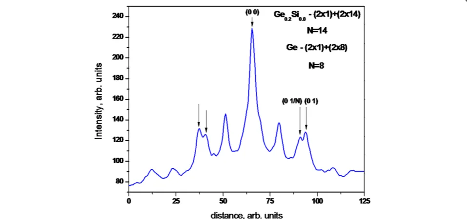
[image:3.595.306.539.90.234.2]The surface morphology of the germanium island film on the surface of GexSi1−xsolid solution changes essen-tially if germanium islands are formed ashutclusters be-fore growing the GexSi1−x layer. The morphology of the GexSi1−x layer located above thehutislands depends on the Ge content in the GexSi1−x layer. The GexSi1−x film is a combination of (2 × 1) and (2 ×n) reconstructions for x < 0.25. On the GexSi1−x surface with concentra-tions x > 0.25, both the above-mentioned reconstruc-tions and the relief of underlying islands are observed. We measured n of (2 × n) reconstruction using our
Figure 2The horizontal profile of the RHEED pattern for GexSi1−xlayer (x= 0.2).
[image:3.595.59.538.488.713.2]software with respect to the video recording of the RHEED pattern during growth (Figure 2). Thenreaches a minimum value of about 8 for clear Ge layer, whereas for GexSi1−x films, n increases from 8 to 14 (Figure 3). The further deposition of the Ge film on the solid solu-tion layer leads to a series of structural transisolu-tions on the surface.
From the kinetic diagram describing the 2D to 3D transition of GexSi1−xfilms, the values located below the 2D to 3D transition revealed the GexSi1−x thickness
region, such that GexSi1−x layers were obtained the 2D dislocation-free pseudomorphic films. The presence of a thin strained GexSi1−x film caused not only changes in critical thicknesses of the transitions, but also affected the properties of the germanium nanocluster array for the top Ge layer. Based on the RHEED data, the shape of the hut-like islands, which were not observed before between the hut and dome islands, was detected. Thus, shaped islands appear on the phase diagram in the range ofx = 0.25 tox= 0.5 (Figure 4). Data were obtained on the growth of Ge/GexSi1−x/Ge heterostructures with the uniform array of islands (standard deviation is approxi-mately 10%) in the second layer of the Ge film.
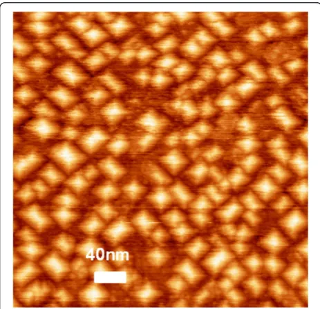
[image:4.595.60.538.88.315.2]The faceting by {105} planes changes upon deposition of several solid solution monolayers. Figure 5 shows an STM image of Ge islands (dGe = 0.3 nm) on Ge0.3Si0.7 (dGeSi= 10 nm)/Ge hut-cluster layers (dGe= 0.6 nm) at 500°C. Germanium islands are formed as square-based pyramids on the solid solution surface similar to those reported in [20]. Their density is lower than the density
[image:4.595.57.289.491.715.2]Figure 4The phase diagram of the growth for Ge/GexSi1−x/Ge heterostructure.
Figure 5STM images of Ge islands.
[image:4.595.304.539.611.706.2]of underlying initial hut clusters (9 × 1010 cm−2). Fur-thermore, bases of the pyramidal islands differ from those of the initial hutclusters; they are 20 nm in char-acteristic size. However, the size distribution of the pyr-amidal islands is much more uniform (approximately by a factor of 2) than that of the germanium hut clusters. The underlying germanium layer causes variations in not only parameters of the island array, but also in their faceting. The RHEED data indicate the presence of facets at a greater angle than plane {105}. While the base edges keep their orientations, these are, supposedly, planes {104} or {103}; their accurate identification needs further studies. The presence of intermediate hut-like shape of the islands is of interest both for structural and topo-logical properties of the surface that affect the optical and electronic properties of the system as a whole.
[image:5.595.305.539.195.670.2]The crystal structure of Ge/GexSi1−x/Si heterolayers with quantum dots was analyzed using cross-sectional high-resolution transmission electron microscopy (TEM). Figure 6 shows a typical TEM image of such kind of het-erostructures. Layers of germanium, solid solution, and silicon are rather different in contrast to allow them to be inspected individually. Neither of the layers contains any defects. Hence, the structure is elastically strained; plastic relaxation does not occur, and the germanium islands are of the characteristichutcluster shape.
Conclusions
The critical thickness of 2D to 3D transition was deter-mined as a function of composition for different growth temperatures during the growth of solid solution GexSi1−x. Non-relaxed atomically smooth GeSi layers were used as an initial surface to fabricate Ge nanoislands. The results obtained make it possible to produce dislocation-free strained heterostructures GexSi1−x, where germa-nium quantum dots reside in quantum wells formed by layers of GeSi solid solution. It is shown that regular pyr-amidal germanium islands with different faceting and array properties are formed on the surface of the solid solution coverage over germaniumhutclusters. Thenof (2 ×n) reconstruction was determined as a function of composition during the growth of solid solution GexSi1−x in the Ge/GexSi1−x/Ge heterostructure. An increase in n from 8 to 14 was believed to take place at the enhance-ment of the Ge content in the GexSi1−xfilm.
Competing interests
The authors declare that they have no competing interests.
Authors' contributions
AIN conceived the study, performed data analysis, and took part in discussions and interpretation of results; he also supervised and coordinated the research projects. VAT participated in the design of the study, carried out the experiments, performed data analysis, and took part in discussions and interpretation of results. SAT investigated the surface morphology by STM and took part in discussions and interpretation of results. AKG performed the HRTEM studies and took part in discussions and interpretation of results. OPP
participated in the design of the study, took part in discussions and interpretation of results, and supervised the research project. All authors read and approved the final manuscript.
Acknowledgments
The work is supported by the Russian Foundation for Basic Research (project no. 12-02-00427, 12-02-31051).
Received: 16 July 2012 Accepted: 29 September 2012 Published: 9 October 2012
References
1. Masini G, Colace L, Assanto G:Germanium-on-silicon infrared detectors.
Encyclopedia of Nanoscience and Nanotechnology2004,3:829. 2. Tao Z, Zhan N, Yang H, Ling Y, Zhong Z, Fang L:The studies of Ge
quantum dots on strained Si0.7Ge0.3 layer by photoluminescence and deep level transient spectroscopy.Appl Surf Sci2009,255:3548. 3. Yakimov AI, Nikiforov AI, Timofeev VA, Bloshkin AA, Kirienko VV,
Dvurechenskii AV:Midinfrared photoresponse of Ge quantum dots on a strained Si0.65Ge0.35 layer.Semicond Sci Technol2011,26:085018. 4. Liu F, Fang W, Lagally MG:Effect of strain on structure and morphology
of ultrathin Ge films on Si(001).Chem Rev1997,97:1045–1061.
5. Matthews JW, Blakeslee AE:Defects in epitaxial multilayers: III. Preparation of almost perfect multilayers.J Cryst Growth1976,32:265.
6. Dodson BW, Tsao JY:Relaxation of strained-layer semiconductor structures via plastic flow.Appl Phys Lett1987,51:1325–1327. 7. Yurasov DV, Drozdov YN:The critical thickness of Stranski-Krastanov
transition with accounted segregation effect.Semiconductors2008, 42:563.
8. Volpi F, Portavoce A, Ronda A, Shi Y, Gay JM, Berbezier I:Nucleation and evolution of Si1−xGexislands on Si(001).Thin Solid Films2000,380:46.
9. Nikiforov AI, Cherepanov VA, Pchelyakov OP, Dvurechenskii AV, Yakimov AI: In situRHEED control of self-organized Ge quantum dots.Thin Solid Films
2000,380:158.
10. Berbezier I, Ronda A, Volpi F, Portavoce A:Morphological evolution of SiGe layers.Surf Sci2003,531:231–243.
11. Baribeau J-M, Wu X, Rowell NL, Lockwood DJ:Ge dots and nanostructures grown epitaxially on Si.J Phys Condens Matter2006,18:R139.
12. Brunner K:Si/Ge nanostructures.Rep Prog Phys2002,65:27. 13. Pchelyakov OP, Yu B, Bolkhovityanov AVD, Nikiforov AI, Yakimov AI,
Voigtlander B:Molecular beam epitaxy of silicon-germanium nanostructures.Thin Solid Films2000,367:75.
14. Yang H, Tao Z, Lin J, Fang L, Zuimin J, Zhenyang Z:Systematic studies of the photoluminescence of Ge quantum dots grown on strained Si0.7Ge0.3buffer layer.Appl Phys Lett2008,9(2):111907.
15. Vostokov NV, Yu N, Drozdov ZFK’n, Lobanov DN, Novikov AV, Yablonski AN, Stoffel M, Denker U, Schmidt OG, Gorbenko OM, Soshnikov IP:Influence of a predeposited Si1–xGexlayer on the growth of self-assembled SiGe/Si (001) islands.Phys Solid State2005,47:26.
16. Lobanov DN, Novikov AV, Vostokov NV, Drozdov YN, Yablonskiy AN, Krasilnik ZF, Stoffel M, Denker U, Schmidt OG:Growth and photoluminescence of self-assembled islands obtained during the deposition of Ge on a strained SiGe layer.Opt Mater2005,27:818. 17. Tersoff J, Tromp RM:Shape transition in growth of strained islands:
spontaneous formation of quantum wires.Phys Rev Lett1993,70:2782. 18. Guo LW, Huang Q, Li YK, Ma SL, Peng CS, Zhou JM:Critical Ge
concentration for 2 ×nreconstruction appearing on GeSi covered Si (100).Surf Sci1998,406:L592–L596.
19. Nikiforov AI, Cherepanov VA, Pchelyakov OP:Oscillation of in-plane lattices constant of Ge islands during molecular beam epitaxy growth on Si.
Mater Sci Eng B2002,89:180.
20. Arapkina LV, Yuryev VA:Atomic structure of Ge quantum dots on the Si (001) surface.JETP Lett2010,91:281.
doi:10.1186/1556-276X-7-561