Technology (IJRASET)
Reconfigurable Fir Filter for Software Defined
Ratio Based On VHBCSE Algorithm
Yuvaraju.M1, Naraina.A2, Sethulaksmi V S3 1
Assistant Professor, Department of EEE, Anna university Regional campus Coimbatore, Tamilnadu, India
2,3
PG Scholor, Department of EEE, Anna university Regional campus Coimbatore, Tamilnadu, India
Abstract: To reduces the number of multiplications per input sample(MPIS) and additions per input sample(APIS) an
optimization technique consist of two-step is used in the design of reconfigurable interpolation filter for multi standard digital up converter(DUC). . For the better efficiency of the constant multiplier a vertical-horizontal binary common sub-expression elimination (VHBCSE) algoritm is used (FIR filter whose coefficient dynamically changes).This reducing the area and as well as power.
Keywords: VHBCSE algoritm, FIR filter, Software defined radio, Digital up converter.
I. INTRODUCTION
Nowadays the communication devices should provide two main features first it should provide global roaming and second is the interfacing with different systems and standards. The existing technologies for different systems such as voice, video, data etc uses different data type, signal processing techniques and packet structures.
According to Joe mitola in 1991“A radio that defines in software its modulation, error correction and encryption processes, which control over the RF hardware and can be reprogrammed is clearly as software defined ratio”.Finite – Impulse Response(FIR) filters is used for variety of tasks such as channel equalization, spectral shaping, interference cancellation and matched filtering
There are various architectures and implementation methods have been proposed to improve speed and performance. The multiplier in the FIR filter defines the performance such as speed and less area of it. An algorithm called multiple constant multiplication has been proposed in the design can be categorized into two groups 1) Graph based algorithms and 2) Common sub-expression elimination (CSE) algorithm.
But MCM design is not suitable for SDR because the filter coefficient in Software define ratio will change system dynamically according to its needs .The coefficients are programmable in SDR and also highly computationally efficient.
Another method used for constant multiplication is binary common sub-expression elimination (BCSE) algorithm. The algorithm can eliminates the common sub-expression in binary. But this algorithm increasing the adder step and also the hardware cost. So this algorithm is insufficient for SDR. Many algorithms like MCM and BCSE are discussed before. In this paper a VHBCSE algorithm is discussed to overcome these problems.
II. MERITS OF USING VERTICAL-HORIZONTAL BINARY COMMON SUB-EXPRESSION ELIMINATION
(VHBCSE) ALGORITM
The vertical-horizontal binary common sub expression elimination (VHBCSE) algorithm solve the problem efficiently that other existing method. The product of original filter coefficient and its complemented value is taken for the signed decimal data representation. This step is done based on the most significant bit of the filter coefficient.
At layer 1 of MAT 2-bit BCSE is applied vertically. After that at layer 2 section 4and 8-bit BCSE’s horizontally is done. This process is done in layer 3also such that hardware usage is reduced .Again this technique is done in the lower layer also which helps to reduce usage of power. Repeated use of 2-bit,4-bit and 8-bit BCSE at different layer also decrease area.
III. DESIGN OF RECONFIGURABLE FIR FILTER
Technology (IJRASET)
clock divided in six equal parts), CLK8 (master clock divided in eight equal parts). The value 4,6,8 are the three interpolation factor represented the three different systems. These 3 clock are used to sample the input RRCIN. The processed architecture consist of data generator (DG), a coefficient generator(CG), a coefficient selector(CS), and an accumulation unit block(FA).
A. Data generator
Data generator task is to sample the input data (RRCIN) based on the interpolation factor selection parameter(INTP_SET), here 7 branch filters are used because the design is for 25, 37 and 49 tap filter (ie,[25 4⁄ ]=[37 6⁄ ]=[49 8⁄ ] =7,here 4,6,8 are the interpolation factor).
B. Co-efficient generator block
The task of coefficient generator block is to multiplexer the input with the coefficient filter. Here a two phase optimization technique is proposed to reduce the hardware usage, low computation time and low complexity. Coefficient generator block consist of first coding pass(FCP unit), second coding pass(SCP unit), partial product generator(PPG unit) and multiplexer unit.First code pass block consist of three coding blocks. These three coding blocks are running according to the three interpolation factor. The output of the first code pass block is given as input to the second code pass block. The output of the second code pass will be the final In the next stage of partial product generator shifting of the data and addition process is executed. This operation gives the multiplication output of input and filter co-efficients sets.
In multiplexer unit and in additional unit summing of partial product generator output is done. This operation is followed by eight multiplexer.
[image:3.612.200.377.334.654.2]
Fig. 1.Block Diagram of Proposed System Architecture
C. Coefficient Selector
The appropriate data which are generated are selected properly and it is provided to the Data accumulation block. The data will be
Co Efficient Selector Data Generator
Co Efficient Generator
Accumulation Unit
clk4 clk6 clk8
INTP_ RESET
FLT RRC_in
Technology (IJRASET)
selected according to the interpolation factor and roll off factor.
D. Data Accumulation Block (FA)
Transposed direct form architecture is used in proposed reconfigurable FIR filter. It consist of six adders and six registers.
IV. VHBCSE ALGORITM
The steps for the vertical-horizontal binary common sub-expression elimination (VHBCSE) algoritm : The inputs of 16 bits (x[15:0]) are received.
17-bit coefficients is stored in look up table,(h[16:0]).
Except the MSB of take the 1’s complement of the coefficient h1[15:0].
Check whether the most significant bit is 1,if it is one the complemented coefficient matrix h[15:0] to generate the multiplexed coefficient matrix m[15:0].
The multiplexed coefficient matrix m[15:0] is divided into static groups of 2bits used for the select lines to M7-M0 multiplexer.
The multiplexer group is again partitioned into 4 bit each matrices (m[15:12],m[11:8], m[7:4], m[3:0]).
Compare the matrices m[15:12] and m[11:8].If they match the output of A2 adder is avoided.Then output of A1 is shitted by 4-bit right and given as an input to adder A5.If they do not match, output of A2 adder is taken instead.
Compare the matrices m[15:12] and m[7:4].If they match the output of A3 adder is avoided.Then output of A1is shifted by 8 bit right and given as an input to A6.Else compare the matrices m[11:8] with h[7:4]if they matches avoid A3 adder’s output use take the 4 bit right shifted output of the adder A2 and give it as input to the adder A6.Else use the output of A3.
Compare the matrices m[15:12] and m[3:0].If they match the output of A4 adder is avoided. Then output of A1is shifted by 12 bit right and given as an input to A6.Else compare m[11:8] with h[3:0] .If they matches avoid A4 adder’s output ,use the 8 bit right shifted output of the adder A2 and give it as input to the adder A6.Otherwise compare the matrices m[7:4] and m[3:0].If they avoid output of adder then avoid output of adder A4 .For that use the 4bit right shifted output of A3 adder and give it to input to adder A4.Else use the A4 adder’s output.
Again partition the multiplexed coefficient into 8 bit group m[15:8],m[7:0].
Compare the matrix m[15:8] and m[7:0].if they matched the output of A6 adder is avoided. For that use the 8 bit right output of A1 adder and give it as an input to A7.Else take adder A6 for output.
The final addition result is performed by 1-bit right shift on the output of the A7 adder. 2”complement of A7 adder is taken.
If 17th bit of MSB of h[16] is 1 then choose the complement otherwise consider the original A7. Multiplication is done .The result is stored in the register.
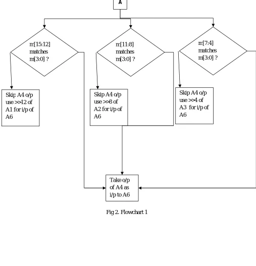
A. Flow Chart Description
The flow chart describes the method of finding h*X in VHBSCE algoritm .In this VHBSCE algoritm first input X[15:0](ie 16 bit input is taken).The 17bits coefficient (ie h[16:0]) is saved in the look up table ie LUT.
The algoritm first check whether 17 bit ie h[16] is ‘1’ or not. If 17 bit is ‘1’ the coefficient matrix is 1’s complemented excluding MSB (that is only 16 bit is 1’s complemented 17th bit is avoided).Thus we get a multiplexed coefficient m[15:0] which is denoted as MC. If 17 bit is ‘0’not ‘1’ then the original version coefficient matrix is taken to produce the multiplexed coefficient(MC),here also the MSB is ignored.
Technology (IJRASET)
Fig 2. Flowchart 1
A
m[15:12] matches m[3:0] ?
Skip A4 o/p use >>12 of A1 for i/p of A6
Take o/p of A4 as i/p to A6
m[11:8] matches m[3:0] ?
m[7:4] matches m[3:0] ?
Skip A4 o/p use >>8 of A2 for i/p of A6
Technology (IJRASET)
Technology (IJRASET)
Again the m[15:12] is compared with m[7:4]. If they matches the output of Adder A1 is right shifted by eight bits and used as the input to Adder A6.The output of Adder A3 is avoided. If the match is not find just use the output of Adder A3 as input of Adder A6. Again compare m[11:8] and m[7:4]. If they matches the output of Adder A2 is right shifted by four bits and used as the input to Adder A6.The output of Adder A2 is avoided. If the match is not find just use the output of Adder A3 as input of Adder A6. After these steps m[15:12] and m[3:0]. If they matches the output of Adder A1 is right shifted by twelve bits and used as the input to Adder A6.The output of Adder A4 is avoided. If the match is not find just use the output of Adder A4 as input as of Adder A6.
Also consider m[11:8] and m[3:0]. If they matches the output of Adder A2 is right shifted by eight bits and used as the input to Adder A6.The output of Adder A4 is avoided. If the match is not find just use the output of Adder A4 as input as of Adder A6. Again consider m[7:4] and m[3:0]. If they matches the output of Adder A3 is right shifted by four bits and used as the input to Adder A6.The output of Adder A4 is avoided. If the match is not find just use the output of Adder A4 as input as of Adder A6.
The MC ie the multiplexer coefficient is again divided into eight of groups m[15:8] and m[7:4].
Technology (IJRASET)
Technology (IJRASET)
Perform the addition in Adder A7 which is denoted as CFC. The 2’s complement of the output of Adder A7 is obtained.
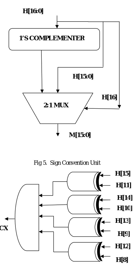
[image:9.612.189.422.128.597.2]If the most significant bit ie 17th bit is ‘1’ take the complemented version otherwise take the original version. At last store the result h*X in h*X register.
Fig 5. Sign Convention Unit
Fig 6. Logic Control Block
CX
H[15]
H[11]
H[10] H[14]
H[9] H[13]
H[8] H[12] 1’S COMPLEMENTER
H[16:0]
2:1 MUX
M[15:0]
Technology (IJRASET)
[image:10.612.202.395.95.643.2]
Technology (IJRASET)
Technology (IJRASET)
V. RESULT AND DISCUSSION
Fig.9 RTL Viewer
The above figure shows the RTL viewer of the VHBSCE algoritm based Reconfigurable FIR filter for SDR.
The next figure shows the waveform generated by the circuit
Fig.10.Simulation Result x[15..0] p8[16..0] p7[14..0] p6[12..0] p5[10..0] p4[8..0] p3[6..0] p2[4..0] p1[2..0] a[16..0] b[16..0] c[16..0] sel[1..0] y[16..0] a[14..0] b[14..0] c[14..0] sel[1..0] y[14..0] a[12..0] b[12..0] c[12..0] sel[1..0] y[12..0] a[10..0] b[10..0] c[10..0] sel[1..0] y[10..0] a[8..0] b[8..0] c[8..0] sel[1..0] y[8..0] a[6..0] b[6..0] c[6..0] sel[1..0] y[6..0] a[4..0] b[4..0] c[4..0] sel[1..0] y[4..0] a[2..0] b[2..0] c[2..0] sel[1..0] y[2..0] a[16..0] b[14..0] s[16..0] a[12..0] b[10..0] s[12..0] a[8..0] b[6..0] s[8..0] a[4..0] b[2..0] s[16..0] a[16..0] b[12..0] s[16..0] a[8..0] b[4..0] s[8..0] a[16..0] b[8..0] s[0..16] sel a[15..0] b[15..0] y[15..0] + A[ 15..0] B[ 15..0] ADDER mux_3 1_11:m14
1' h0 2' h0
--mu x_31 _9:m15
1' h0 2' h0
--mu x_31 _7:m16
1' h0 2' h0
--mu x_31 _5:m17
1' h0 2' h0
--mu x_31 _3:m18
1' h0 2' h0
--add17:a1
add13:a2
add9:a3
add5:a4 a dd9_5:a22 add17_9:a31
mux_21:m31 Add0
16' h0001
--x[15..0]
y[16..0]
z[32..0]
1' h0 16' h0000
--ppg:p11 mux_3 1_17:m11
1' h0 2' h0
--mux_3 1_15:m12
1' h0 2' h0
--mux_3 1_13:m13
1' h0 2' h0
Technology (IJRASET)
VI. CONCLUSION
The proposed reconfigurable filter architecture suitable for multistandard DUC, the important component of SDR. Here a two step optimization technique is used to make the desired filter more efficient by reducing area and power along with improvement in the maximum operating frequency. The proposed constant multiplier based on VHBCSE algorithm will maximize the efficiency and this algorithm also supports the signed decimal data representation of input and coefficient. This system is more suitable for next generation efficient system of SDR.
VII. ACKNOWLEDGEMENT
This research and material reported in this document are supported by the Anna university regional campus Coimbatore.
REFERENCES
[1] J. Mitola, “The software radio architecture,” IEEE Commun. Mag., vol. 33, no. 5, pp. 26–38, May 1995.
[2] Hatai, Indranil, Indrajit Chakrabarti, and Swapna Banerjee. "An Efficient Constant Multiplier Architecture Based on Vertical-Horizontal Binary Common Sub- expression Elimination Algoritm for Reconfigurable FIR Filter Synthesis", IEEE Transactions on Circuits and Systems I Regular Papers, 2015.
[3] S. Im, W. Lee, C. Kim, Y. Shin, S. H. Lee, and J. Chung, “Implementation of SDR-eared digital IF channelized dechannelizer for multiple CDMA signals,” IEICE Trans. Commun., vol. E83-B, no. 6, pp. 1282–1289, Jun. 2000.
[4] S.-F. Lin, S.-C.Huang, F.-S.Yang, C.-W.Ku, and L.-G. Chen, “Power-efficient FIR filter architecture design for wireless embedded system,” IEEE Trans.
Circuits Syst. II, Exp. Briefs, vol. 51, no. 1, pp. 21–25, Jan. 2004.
[5] Y. Son, K. Ryoo, and Y. Kim, “1:4 interpolation FIR filter,” IEEE Electron.Lett., vol. 40, no. 25, pp. 1570–1572, Dec. 2004.
[6] P. K. Meher, S. Chandrasekaran, and A. Amira, “FPGA realization of FIR filters by efficient and flexible systolization using distributed aritmetic,” IEEE Trans. Signal Process., vol. 56, no. 7, pp. 3009–3017, Ju l. 2008.
[7] J. Xie, J. He, and G. Tan, “FPGA realization of FIR filters for high-speed and medium-speed by using modified distributed aritmetic architectures,” Microelectron. J., vol. 41, no. 6, pp. 365–371, Jun. 2010.
[8] K.-H. Chen and T.-D.Chieueh, “A low-power digit-based reconfigurable FIR filter,” IEEE Trans. Circuits Syst. II, Exp. Briefs, vol. 53, no. 8, pp. 617–621, Aug. 2006.
[9] O. Gustafsson, “Lower bounds for constant multiplication problems,” IEEE Trans. Circuits Syst. II, Exp. Briefs, vol. 54, no. 11, pp. 974–978, Nov. 2007. [10] D. Shi and Y. J. Yu, “Design of linear phase FIR filters with high probability of achieving minimum number of adders,” IEEE Trans. Circuits Syst. I, Reg.