Technology (IJRASET)
Tapped Inductor Quasi-Z-source Inverter
With High Inversion Gain
V. Malathi#1, K. Venkatesan*2
#1
Research Scholar, Department of EEE, SCSVMV University, Kanchipuram-631 561, Tamil Nadu, India.
*2
Associate Professor, Department of EEE, Prathyusha Engineering College, Aranvoyal Kuppam, Thiruvallur-602 025, Tamil Nadu, India.
Abstract—This paper proposes a high inversion gain single stage boost inverter, which introduces a tapped inductor network into the traditional quasi-Z-source inverter (qZSI), called tapped inductor quasi-Z-source inverter (TL-qZSI). The tapped inductor network including one tapped inductor and two diodes and is used to replace one inductor of the traditional qZSI. Similar to the tapped inductor Z-source inverter (TL-ZSI), the proposed inverter can provide high inversion gain. TL-qZSI has all the merits of TL-ZSI except that it also features with continuous input current, common ground with the dc source, and reduced capacitor voltage stress. This paper analyses the circuit operation principle, boost inversion features and its control strategy. Simulation and Experimental results are provided to verify its effectiveness and demonstrate the real features of the proposed circuit.
Keywords— Pulse Width Modulation; Switched Inductor Quasi z Source Inverter; Unipolar PWM.
I. INTRODUCTION
Traditional voltage-source PWM inverter (VSI) is generally a buck-type converter. One of its characteristics is that the instantaneous output voltage is always lower than the dc input. In applications with wide input voltages, such as distributed power generation (DG) systems, a boost type DCDC converter is often added in front of the VSI to step up the dc input voltage [1]-[3] in case of a low level dc input. However, the traditional boost converter may not be able to provide enough dc voltage gain even for an extreme duty cycle. Large duty cycle operation may result in serious reverse-recovery problem and increase the rating of power devices. And also this two stage operation solution will inevitably increase the overall cost and system complexity, and deteriorate system efficiency. On the other hand, the upper and lower devices of the same phase leg cannot be gated on simultaneously in the traditional VSI. Otherwise, shoot through problem would occur and destroy the switching devices. Dead time is always used in case of shoot-through events in bridge-type converters, but it will cause waveform distortion. Though dead-time compensation technology [4]-[5] has been developed, it increases the control complexity. So it is desirable to have a single-stage boost inverter featuring with no shoot through issues. Z-source inverter (ZSI) [6] was proposed to overcome the issues of the traditional inverters, shown in Fig. 1(a). It is a single-stage inverter topology to demonstrate both buck and boost power conversion ability by gating on the two switches in the same phase leg simultaneously. Due to shooting through the phase legs becomes a normal operation mode, the bridge shoot-through is no longer an issue, but utilized as a control variable and is defined as “shoot-through zero state”. So the reliability can be improved. Boost factor B of Z-source inverter can be expressed as:
(1)
where Vi is the dc input voltage, b v is the amplitude of bus voltage, and D0 is the shoot-through duty cycle. It is clear that D0 is confined between 0 and 0.5 when B varies between 1 and ∞. The upper extreme is unachievable in practice, which would push down the voltage gain of whole converter to a much lower value [7]-[9]. Fig. 1(b) shows one of the voltage-fed quasi-Z-source inverter [10] with continuous input current. It also features with a common ground with the dc input source, and lower capacitor voltage stress. Boost factor of qZSI is the same with that of ZSI.
Technology (IJRASET)
content [9]. In other words, a smaller modulation index would lead to a smaller overall inversion gain and deteriorate circuit performance. Recent researches on its improvement of boost inversion ability have been proposed in [11]-[16]. The extended-boost qZSI [11] including diode-assisted boost and capacitor assisted boost source inverter, extend the boost ability of quasi-Z-source inverter. In practice, they are cascaded quasi-Z-quasi-Z-source impedance networks with very complex circuit configuration. In [12] and [13], coupled inductor is introduced to provide high boost inversion ability by introducing turns ratio of the coupled inductor as a control variable.
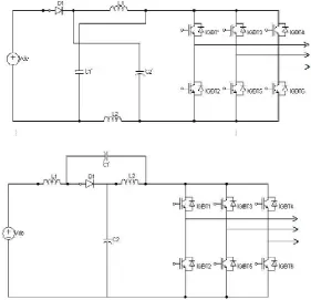
Fig.1. (a) Traditional Z-source inverter and (b) quasi-Z-source inverter with continuous input current.
One advantage of this converter is that the component count is reduced. However, it still cannot avoid its practical limit arising from the leakage inductance even if it is very small. Applying capacitor, inductor, and hybrid switched-capacitor/inductor structures of the high boost gain dc-dc converter, a switched inductor (SL) cell is introduced to combine with the traditional ZSI [14] and qZSI [15] to improve the impedance-type inverters’ boost inversion performance. The modified switched-inductor, called tapped switched-inductor, and ZSI of this type is introduced in [16]-[17], which is generally less complex. This paper proposes a new tapped inductor quasi-Z-source inverter. It introduces an impedance network including a tapped inductor and two diodes to replace one inductor of the traditional qZSI. The new converter can improve the boost inversion ability of the traditional qZSI, together with a voltage-buck freedom. This is achieved by using shoot through zero state defined in the traditional ZSI, and also by properly designing the tapping position of the inductor. In the following sections, operation principle, boost inversion feature and control strategy of the proposed converter will be analyzed in detail. Simulation and experimental results are shown to verify the correctness and effectiveness.
II. THETAPPEDINDUCTORZ-SOURCEINVERTER
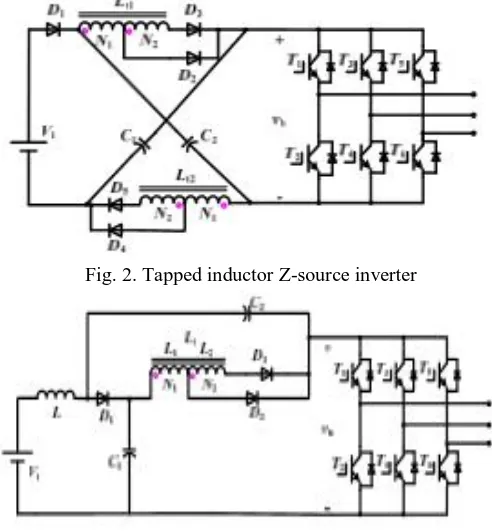
Fig. 2 shows the general structure of the tapped inductor Z-source inverter [17]. It obtains high voltage conversion gain with a relative short shoot-through zero state, which improves power quality of the circuit. The switched tapped inductor network composes of four diodes and two tapped inductor cells and is introduced to replace the two inductors of the traditional ZSI. The boost factor can be increased by simply changing the tapping position. Boost factor B of this inverter is
[image:3.612.160.441.171.442.2]Technology (IJRASET)
where N is turns ratio of the tapped inductor, supposing coupling coefficient is unity. In order to make the achievable boost inversion operation, the shoot-through duty cycle should be limited to () 0<1 2D N + . Unlike traditional ZSI, boost factor of this converter is influenced by both shoot-through duty cycle D0 and turns ratio N whose value can be freely varied by changing the TL tapping position. Although the boost inversion ability is improved, the TL-ZSI has several drawbacks: 1) it adds four diodes and two tapped inductors, compared with traditional ZSI, which obviously increases system size and cost; 2) it requires a LC network in the front end to reduce the input current ripple because of its current discontinuity.
III.PROPOSEDTAPPEDINDUCTORQUASI-Z-SOURCEINVERTER
[image:4.612.186.432.275.541.2]Fig. 3 shows the proposed tapped inductor quasi-Z-source inverter (TL-qZSI). The combination of Lt, D2, and D3 acts as a switched tapped inductor cell. Compared to the traditional quasi-Z-source inverter with continuous input current, only one tapped inductor and two diodes are added. This configuration allows the impedance network with different inductances under shoot-through state and non-shoot-through state. Only the inductance of winding N1 is effective during the shoot-through zero state, while both the inductances of winding N1 and N2 are effective during the non-shoot-through state. It is impossible for the tapped inductor to achieve a complete coupling effect, so leakage inductance exists in the real circuit as shown in Fig. 4. As the turns ratio can be defined as N=N2/N1. The leakage inductor Lk and magnetizing inductor Lm can be described as [18]-[19]
Fig. 2. Tapped inductor Z-source inverter
Fig. 3. Tapped inductor quasi-Z-source inverter
(3)
(4)
where k is the coupling coefficient. Then the inductance of tapped inductor can be expressed as
(5)
Technology (IJRASET)
Like the traditional ZSI, the proposed inverter has the extra shoot-through zero states besides the traditional six active and two open-zero states. By regulating the shoot-through open-zero states when circuit parameters are designed, the energy is stored and transferred within the impedance network to boost the amplitude of the bus voltage. It should be noted that shoot through zero states are allocated into open-zero states without changing the total open-zero state and active state time intervals.
IV.OPERATIONPRINCIPLE,BOOSTINVERSIONFEATUREANDITSCONTROL
A. Operation Principle
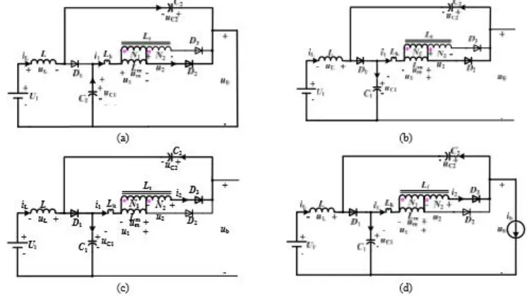
[image:5.612.124.497.216.426.2]Assuming that the capacitances of C1 and C2 are sufficiently large, and then the capacitor voltages are almost constant. Fig. 4 shows the equivalent circuits of TL-qZSI under different states. Operation principle can be briefly described in these switching states.
Fig. 4. Equivalent circuit under three switching states: (a) shoot-through zero state, (b), (c) open-zero state, and (d) active state.
1) State 1: The converter is in shoot-through zero state under this duration, as shown in Fig. 4(a). A short circuit has been explicitly
drawn in place of the dc bus viewed from the TL network and vb=0. Input dc source voltage and capacitor C2 voltage is applied across inductor L, making inductor L current linearly increase, vL=Vi+VC2. Voltage applied across winding N1 is reflected to winding N2, and v2=Nvm= Nk2VC1, leading to diode D3 reverse biased. Diode D1 also becomes reverse biased, due to VC1>-VC2. Voltage of winding N1 in shoot-through zero state is only related to capacitor C1.
2) State 2: During this time interval, the converter is in one of the two traditional open-zero states, as shown in Fig. 4(b), (c). C1 is
charged by L and input dc source Vi, therefore vL=VC1-Vi. In the initial time, leakage inductor Lk and capacitor C2 start to resonate. After the resonant current decreases to a certain value, winding N2 reverses its polarity causing diode D3 to become forward biased. The magnetizing current is reflected to winding N2. Winding N2 series with the winding N1 and transfers the earlier stored magnetizing energy to capacitor C2. Diode D2 turns off naturally.
3) State 3: During this time interval, the converter is operating in the active state, as shown in Fig. 4(d). The inverter bridge can be
viewed as a current source. Winding N2 series with winding N1 and transfers the earlier stored magnetizing energy to the load. And the bus voltage is stepped up. Capacitor C 1 is continuously charged by L and input dc source Vi, therefore vL=VC1-Vi.
B. Boost Inversion Feature Analysis
Technology (IJRASET)
(7)
Define the resonant time interval of the leakage inductor and C2 as T1, and T1=D1Ts. The voltage across winding N1 during T1 can be expressed as
(8)
After T1, winding N2 reverses its polarity and series with winding N1 to transfer energy. Define the time interval of state 3 as T2, and T2=(1-D0-D1) Ts. The voltage of winding N1 is
(9)
which can be simplified as
(10)
The average voltage across winding N1 of the tapped inductor can be expressed as
(11)
The voltages across inductor L during T0, T1+T2 time intervals are described in “operation principle” section. The average voltage of inductor L can be expressed as
(12)
Combining (11) and (12), then the voltage across C1 and C2 can be derived as
(13)
(14)
While the bus voltage amplitude can be expressed as
(15) Boost factor B = Vb/Vi can be obtained from (13), (14), and (15)
(16)
It is desired to have a tightly coupled inductor to achieve higher boost factor. Supposing the tapped inductor is of completely coupled, the boost factor can be expressed as
(17)
The shoot-through duty cycle is limited to , and N is getting larger while D0 is getting smaller. The boost factor
Technology (IJRASET)
C. Control Strategy
The basic PWM control methods, including simple, maximum, and constant boost control, are all fit for the proposed TL-qZSI. For simple boost control method, the maximum shoot-through duty cycle equals to 1-m. The voltage gain G of the whole converter can then be expressed as:
(18)
The peak value of the output phase voltage can be expressed as
[image:7.612.225.384.275.416.2](19)
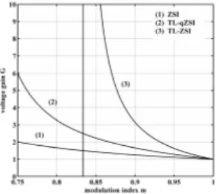
Fig. 6 shows the voltage gain versus modulation index of different topologies under simple boost control method when k=1. For the same voltage gain, the modulation index of the proposed inverter is higher than that of the traditional ZSI, leading to improved THD of output phase voltage. While the modulation index of the proposed inverter is lower than that of TL-ZSI.
Fig. 5. Boost factor comparison of different topologies when k=1.
Fig. 6. Voltage gain comparison of different topologies when k=1.
V. SIMULATIONANDEXPERIMENTALRESULTS
[image:7.612.230.387.443.582.2]Technology (IJRASET)
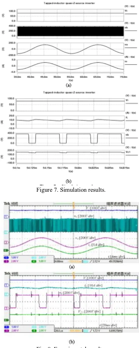
When the input voltage is low, the shoot-through zero state was regulated to boost the amplitude of the bus voltage to 390V, enough to output the desired ac voltage. The voltage and current stresses are consistent with the analysis above. Both the input voltage and the voltage stress of capacitor C1 are lower than the reported results of quasi-Z-source inverter
in [10], given the same output voltage. By controlling the shoot-through duty cycle D0 or the boost factor B when the tapped inductor parameters has been designed, the desired output ac voltage can be obtained even when the input voltage is at a low level.
[image:8.612.195.423.144.713.2]Figure 7. Simulation results.
Technology (IJRASET)
VI.CONCLUSION
This paper has proposed a tapped inductor quasi-Z-source inverter (TL-qZSI) which improving the boost inversion ability of the traditional qZSI. The proposed converter introduces an impedance network with tapped inductor to couple the low dc input voltage source to the inverter bridge. The boost ability is decided by the tapping positions and the shoot-through zero state. Turns ratio and leakage inductance of the tapped inductor affect the performance of whole inverter greatly. The proposed converter has some merits.
A. By designing the tapped inductor properly and adjusting the previously forbidden shoot-through zero state, the amplitude of the bus voltage can be greatly stepped up and the boost inversion ability of the whole inverter can be greatly improved.
B. By inheriting the unique “shoot-through” time interval of the traditional ZSI, the reliability of whole invertercan be improved.
C. Input current of the proposed converter is continuous. Capacitor voltage stresses are reduced, and component count is minimized compared to traditional ZSI.
D. The concepts of TL quasi-Z-source impedance network can also be applied to ac-dc, ac-ac, and dc-dc power conversion.
REFERENCES
[1] Mohr. M, Franke. W. T., Wittig. B., et al, “Converter systems for fuel cells in the medium power range—a comparativestudy,” IEEE Transactions on Industrial Electronics, vol. 57, no. 6, pp. 2024-2032, June. 2010.
[2] Rong-Jong Wai, Wen-Hung Wang, Chung-You Lin, “Highperformance stand-alone photovoltaic generation system,” IEEE Transactions on Industrial Electronics, vol. 55, no. 1, pp. 240-250, Jan. 2008.
[3] Bo Yang, Yi Zhao, Xiangning He, et al, “Design and analysis of a gridconnected photovoltaic power system,” IEEE Transactions on Power Electronics, vol. 25, no. 4, pp. 992-1000, Apr. 2010.
[4] Seon-Hwan Hwang, Jang-Mok Kim, “Dead time compensation method for voltage-fed PWM inverter,” IEEE Transactions on Energy Conversion, vol. 25, no. 1, pp. 1-10, Mar. 2010.
[5] Lihua Chen, Fang Zheng Peng, “Dead-time elimination for voltage source inverters,” IEEE Transactions on Power Electronics, vol. 23, no. 2, pp. 191-197, March 2008.
[6] F. Z. Peng, “Z-source inverter,” IEEE Transactions on Industry. Application, vol. 39, no. 2, pp. 504-510, Mar. 2003.
[7] Fang Zheng Peng, Miaosen Shen, and Zhaoming Qian, “Maximum boost control of the z-source inverter,” IEEE Transactions on Power Electronics, vol. 20, no. 4, pp. 833-838, July 2005.
[8] Miaosen Shen, Jin Wang, Alan Joseph, and F. Z. Peng, “Constant boost control of the z-source inverter to minimize current ripple and voltage stress,” IEEE Transactions on Industrial Electronics, vol. 42, no. 3, pp. 770-778, May/June 2006.
[9] Poh, Chiang Loh, Vilathgamuwa, D. M., Lai, Y. S., et al., “Pulse-width modulation of Z-source inverters,” IEEE Transactions on Power Electronics, vol. 20, no. 6, pp.1346-1355, Nov. 2005.
[10] Joel Anderson, Peng F. Z., “Four quasi-Z-source inverters,” in Proc. IEEE Power Electronics Specialists Conf., 2008, pp.2743-2749.
[11] Gajanayake C. J., Fang Lin Luo, Hoay Beng Gooi, et al, “Extendedboost Z-source inverters,” IEEE Transactions on Power Electronics., vol. 25, no. 10, pp. 2642-2652, Oct. 2010.
[12] R. Strzelecki, M. Adamowicz, N. Strzelecka, and W. Bury, "New type T-Source inverter," in Proc. Compatibility and Power Electronics, Conf., 2009, pp. 191-195.
[13] Wei Qian, Fang Zheng Peng, and Honnyong Cha, “Trans-Z-source inverters,” in Proc. Power Electronics Conf., 2010, pp. 1874-1881.
[14] M. Zhu, K. Yu, and F. L. Luo, "Switched Inductor Z-Source Inverter,“, IEEE Transactions on Power Electronics, vol. 25, no. 8, pp. 21502158, Aug. 2010. [15] Nguyen M., Lim Y., and Cho G., “Switched-inductor quasi-Z-source inverter,” IEEE Transactions on Power Electronics, in press, 2011.
[16] Ding Li, Poh Chiang Loh, Miao Zhu, and et. al., “Cascaded switchedinductor and tapped-inductor z-source inverters,” in Proc. Applied Power Electronics Conf., 2011, pp. 1661-1666.
[17] Miao Zhu, Ding Li, Poh Chiang Loh, et. al., “Tapped-inductor z-source inverters with enhanced voltage boost inversion abilities,” in Proc. Sustainable Energy Technologies Conf., 2010, pp. 1-6.
[18] Robert W. Erickson, Dragan Maksimovic, “Fundamentals of Power Electronics(second edition),” Norwell, MA: Kluwer, pp. 502-505, 2001.
[19] Xavier Margueron, Jean-Pierre Keradec, “Design of equivalent circuits and characterization strategy for n-input coupled inductors,” IEEE Transactions on Industrial Electronics, vol. 43, no. 1, pp. 14-22, Jan/Feb 2007.