2019 2nd International Conference on Informatics, Control and Automation (ICA 2019) ISBN: 978-1-60595-637-4
Comparative Study on the Forbidden States of the SR Flip-flops
Xiao-dong LIU
1,*, Jian-long FU
1and Li-ping TU
21
School of Physical Science and Technology, Tianjin Polytechnic University, Tianjin 300387, China
2
Engineering Teaching Practice Training Center, Tianjin Polytechnic University, Tianjin 300387, China
*Corresponding author
Keywords: SR latch, Synchronous SR flip-flop, Master-slave SR flip-flop, Forbidden state, Both 0 state, Both 1 state.
Abstract. In the teaching process of “Digital Electronic Technology” or “Digital Circuit” in colleges
and universities, it is usually necessary to teach the forbidden states of the two “basic SR latches”, the “synchronous SR flip-flops”, the “master-slave SR flip-flop” and the “standard SR flip-flop” that do not satisfy the constraint condition. However, it is found in the examination of various teaching materials, many teachers have a vague understanding of the corresponding forbidden state, thus giving the wrong way of speaking. This paper gives a comparative analysis of various forbidden states, trying to clarify the ambiguity about them. Further, four new names of “both 0 state (or third state)” and “both 1 state (or fourth state)” are suggested, and suggestions for the correct truth table of the corresponding forbidden state in various situations are given. This paper is expected to play a positive role in the teaching of the electronic technology basic courses and in the preparation, re-preparation and publication of teaching materials.
Introduction
In the teaching of “Digital Electronic Technology” or “Digital Circuits” in colleges and universities (hereinafter referred to as “digital circuits”), the “Basic SR Latches” and modified “Level-triggered SR flip-flop (FF)” (synchronous SR FF) and the “master-slave SR FF” are generally taught [1-12], and they all involve the constraints they are to satisfy. For example, for the basic SR latch composed of “NOR gates”, the constraint condition to be satisfied is SR = 0, which corresponds to the three allowed cases, and the corresponding forbidden condition is the remaining fourth case: SR = 1. Here, since the asynchronous setting is not involved, the symbol system SD/RD is not used.
However, in the examination of the teaching methods of the existing various textbooks, it is found that many teachers have a vague understanding of the corresponding forbidden (prohibition) state, thus give the wrong way of the expository teaching. This paper gives a comparative analysis of various prohibited states, trying to clarify their ambiguity about these forbidden states.
Forbidden State of the Basic SR Latch
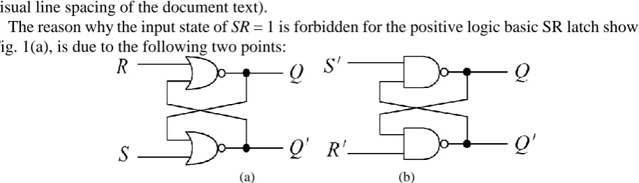
Figure 1 (a) and (b) show two basic SR latch circuits [1] composed of "NOR gate" and "NAND gate", respectively, which are referred to as positive and negative logic basic SR latches, respectively, because the set signal is high for the former and the set signal is low for the latter. This name has not been found in the textbook and is recommended for readers here.
For the positive logic basic SR latch shown in Fig. 1(a), the input constraint to be satisfied is SR = 0, corresponding to three allowable cases: S = 1, R = 0, setting (set 1: Q* = 1, Q'* = 0) function; S = 0, R
is slightly more complicated and usually requires the use of an “formula editor” that changes the visual line spacing of the document text).
The reason why the input state of SR = 1 is forbidden for the positive logic basic SR latch shown in Fig. 1(a), is due to the following two points:
(a) (b)
Figure 1. (a) Positive logic (b) Negative logic circuits of the basic SR latch.
(1) Although the final state of the latch is definite and stable, i.e., Q* = 0, Q'* = 0, in the stable input state of SR = 1, but it is not the standard “1 state (Q = 1, Q' = 0)” or “0 state (Q = 0, Q' = 1)”. In this paper, the author calls it “both 0 state” or the third statesuggested by us, and it is recommended to be widely used in textbooks. The appearance of this state allows students to understand that the latch is as “incompatible” as “Brundan's nephew”, so “reverse” the requirement of S = 1 to get Q* = 0, “reverse” the requirement of R = 1 to gives Q'* = 0.
(2) The next state Q**/Q'** of the latch Q*/Q'* state will become uncertain after S = 1 and R = 1 disappear (become the low level) for three reasons (abbreviated as “uncertain”): (a) S = 1 and R = 1 disappear at different times ( there are other words of “sooner or later” and “faster and slower”, this article appreciates the word “time-sharing”); (b) there is a transportation-delay difference between the two “NOR gates” (the reason of the race-risk phenomenon), and (c) there is a load difference (such as the different effective capacitance at the Q and Q' ports). However, this “uncertain” state is ultimately determined, and once is formed, it is the standard “1 state” or “0 state” and is held on.
Therefore, it is correct and common to make a “forbidden (prohibited or not allowed)” comment at the corresponding position Q* = 0, Q'* = 0 in the truth table of the positive logic basic SR latch. However, in the examination of the truth tables of various existing textbooks, it was found that too many authors made the following mistakes, assumed as a matter of course, or been wrongly informed: (1) Disregarding the fact that the latch state is an explicit “both 0 state”, and the final state at corresponding position of the “truth / function table” is directly written as “uncertain” or “x”, or even unconditionally written as “forbidden”.
(2) Even if the final state of the latch is clearly marked as “both 0 state” (written as “both 1 state”, it can be understood as a miswriting), but the remarks under the truth / function table only indicate only one or two of the above-mentioned three reasons that cause the latch state to be uncertain.
(3) Assume that the S and R high-level signals disappear “simultaneously”, but still use the inconsistent assumption that “one of high-level signals disappear first”, and many more.
As for the negative logic basic SR latch shown in Fig. 1(b), the forbidden conditions are S' = 0 and
R' = 0, which are actually also equivalent to SR = 1. The reason why the input states of S' = 0 and R' = 0 at the same time are disabled is similar to the abovementioned case of the positive logic basic SR latch, except that:
(1) The final state of the latch is a clear “both 1 state” (or the fourth state suggested by us): Q* = 1,
Q'* = 1, because the latch impartially “obey” the setting requirement of S' = 0 and the resetting requirement of R' = 0 to result in Q* = 1 and Q'* = 1.
(2) After both S' = 0 and R' = 0 disappear (become high-levels), the state of the latch becomes uncertain due to the above three reasons.
[image:2.595.63.521.90.221.2]Forbidden State of the Synchronous SR FF
[image:3.595.181.413.152.262.2]Usually, a positive logic synchronous SR FF is formed through improving a negative logic NAND basic SR latch composed of two NAND gates by using two NAND gates (substantially not improving a positive logic basic SR latch by using two NAND gates to be a negative logic synchronous SR FF), as shown in Figure 2 [1].
Figure 2. Circuit of the Synchronous SR FF.
The discussion on the forbidden condition and state of the synchronous SR FF is more complicated because the CLK is in the same position as the S/R input. During the duration of CLK = 1, the situation is similar to the two basic SR latches described above, but the FF “follows” the requirement of S/R = 1 to get the “both 1 state” (the fourth state).
The added complexity or problem is that during the duration of SR = 1, after CLK = 0, for G1, 2 due
to the difference in transmission delay between the two pairs of NAND gates (because of the race-risk phenomenon: the outputs of G1, 2 can become either the standard setting signal, or a standard reset
signal), it can also cause the final state of the FF to become uncertain. Of course, this “uncertain” state is finally maintained once it is formed, which is the standard “1 state” or “0 state”, not the third, forth or unstable state.
Therefore, when the teaching activity is conducted on the synchronous SR FF, you should be able to express these two problems correctly and completely.
Forbidden State of the Master-slave SR FF
As a further improvement to the synchronous SR FF, the pulse-triggered master-slave SR FF circuit is shown in Figure 3 [1].
Figure 3. Circuit of the master-slave SR FF.
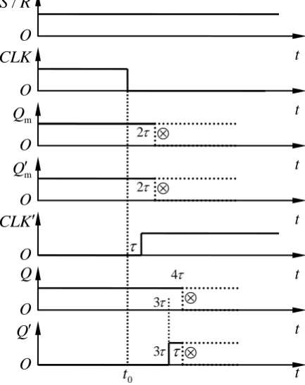
The discussion of the forbidden condition and state of the master-slave SR FF is further more complicated than the synchronous SR FF because the path from the S/R/CLK signal to the input ports of the slave SR FF that ultimately determines the Q/Q' state of the master-slave SR FF is more complicated. Here, we will not discuss the forbidden state of the “master” SR FF state caused by the disappearance of S = R = 1 during the existence of CLK = 1.
Assume that the propagation delays of all eight NAND gates G1~8 and NOT gates G9 (here we can
[image:3.595.143.451.529.660.2]of the master-slave SR FF (i.e. the state of the slave FF) is “1 state” (Q' = 0), then the
[image:4.595.189.406.115.389.2]CLK/Qm/Q'm/CLK'/Q/Q' logic level waveformsafter CLK = 0 at time t0 are shown in Figure 4.
Figure 4. Logic level waveform of the master-slave SR FF before and after CLK = 0.
It can be seen from Fig. 4 that after τ the clock signal CLK' = 1 of the slave SR FF is reached. Since the state of the master SR FF is “both 1 state (the fourth state)”, then when 2τ is passed, the state of the slave SR FF also becomes a clear “both 1 state”, but this state can only maintain a short time τ. Because the master SR FF is the aforementioned synchronous SR FF, the “both 1 state” of the master SR FF can only hold for 2τ, and the state is “uncertain” after 2τ from CLK = 0 at time t0 , so that after
another 2τ, the state of the slave SR FF has also become uncertain.
Therefore, under the forbidden condition (SR = 1), after the clock pulse disappears, the steady state of the master-slave SR FF, similar to the synchronous SR FF, is the “uncertain” state, while the state of the positive/negative logic basic SR latch is a certain “both 0 state” (third state) or “both 1 state” (forth state), except that the state of basic SR FF become uncertain after the S/R = 1 disappears.
Forbidden State of the Standard SR FF
When studying the logical function description of the SR FF, the so-called “standard SR FF” is generally discussed, that is, the setting/resetting/holding operations work according to the positive logic, and the specific triggering mode (level-triggered, pulse-triggered and edge-triggered modes) is not discussed, one does not distinguish between the “0 state”, “1 state”, “both 0 state” or “both 1 state” before the clock is applied under the forbidden condition. It is considered that after the clock is active, the steady state is uncertain, and therefore it is forbidden.
Description Collection of Prohibited States of Various SR FFs
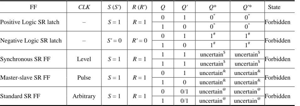
Thus, the forbidden states and notes about them of the five cases (positive/negative logic SR latch and synchronous/master-slave/standard SR FF) are summarized in Table 1 for reference.
CLK
/
S R
m Q
m Q
Q
Q
CLK t
t
t
t
t
t
t
3 2
2
3 O
O O O O O O
0 t
Table 1. Collection of the forbidden states and notes about them of positive/negative logic SR latches and synchronous/master-slave/standard SR FFs for the correct truth / function table and comments.
FF CLK S (S') R (R') Q Q' Q* Q'* State
Positive Logic SR latch – S = 1 R = 1 0 1 0
* 0*
Forbidden
1 0 0* 0*
Negative Logic SR latch – S' = 0 R' = 0 0 1 1
# 1#
Forbidden
1 0 1# 1#
Synchronous SR FF Level S = 1 R = 1 1 1 uncertain
$
uncertain$
Forbidden 1 1 uncertain$ uncertain$
Master-slave SR FF Pulse S = 1 R = 1 0 1 uncertain
& uncertain&
Forbidden 1 0 uncertain& uncertain&
Standard SR FF Arbitrary S = 1 R = 1 0 0/1 uncertain
@ uncertain@
Forbidden 1 0/1 uncertain@ uncertain@
Notes:
*“Both 0 state” (third state), but the final state is uncertain after the both S =1 and R = 1 signals disappear synchronously
or asynchronously.
# “Both 1 state” (forth state), but the final state is uncertain after the both S' =0 and R' = 0 signals disappear
synchronously or asynchronously.
$ The final state is uncertain when (1) the state of both S = 1 and R = 1 disappear during the period of CLK = 1, (2) CLK
disappears with S = R = 1 signals existing all the way.
&
The “master” FF is at “both 1 state” CLK = 1 during, but is uncertain after both S =1 and R = 1 signals disappear; when
S = R = 1 signals exist, and CLK becomes to be 0, the slave FF is first at “both 1 state”, and then quickly becomes uncertain due to the “both 1 state” of the master FF.
@
Uncertain state because of the abovementioned * and # notes, regardless of the triggering method.
Summary
The two “basic SR latches”, “synchronous SR flip-flops”, “master-slave SR flip-flops” and the so-called “standard SR flip-flops” have the corresponding forbidden condition S = R = 1. In this paper a comparative analysis of various forbidden states is given, trying to clarify the ambiguity of them. Further, four new definitions of “both 0 state (or third state)” and “both state (or fourth state)” are suggested, and the correct truth/function table of the corresponding forbidden state part of each case is given. We hope that this paper can play a positive role in the teaching of the basic course and the preparation, reprinting and publication of the related textbooks.
Acknowledgement
This research was financially supported by the Returned Overseas Chinese Research Fund from the Ministry of Education (48th).
References
[1] S. Yan, Digital Electronic Technology Foundation, sixth ed., Higher Education Press, Beijing, 2016.
[2] W.N. Li, L.H. Su, Digital Electronic Technology Foundation, China Electric Power Press, Beijing, 2016.
[3] C.L. Yang, S.J. Wang, Digital Electronic Technology Foundation, Tsinghua University Press, Beijing, 2107.
[5] X. L. Chen, W. He, Digital Electronic Technology Foundation, Tsinghua University Press, Beijing, 2018.
[6] Y.C. Wang, X.L. Wu, Digital Electronic Technology Foundation, Anhui University Press, Hefei, 2018.
[7] P. Wang, Digital Electronic Technology Foundation, Mechanical Industry Press, Beijing, 2019.
[8] R.Y. Shen, Digital Electronic Technology Foundation, second ed., Mechanical Industry Press, Beijing, 2019.
[9] G.W. Gao, Digital Electronic Technology Foundation, second ed., China Electric Power Press, Beijing, 2019.
[10] H. An, Digital Electronic Technology Foundation and Practice, Xi'an University of Electronic Science and Technology Press, Xi'an, 2019.
[11] X.X. Shen, Digital Electronic Technology, China Railway Publishing House, Beijing, 2019.