2019 International Conference on Applied Mathematics, Modeling, Simulation and Optimization (AMMSO 2019) ISBN: 978-1-60595-631-2
Research on Modeling Simulation and Parameters Extraction of IGBT
Huan-yao QIN
1, Hong-min GAO
1,*and Guang-yu LI
21
School of Information and Electronics, Beijing Institute of Technology, Beijing China 2
Beijing Research Institute of Mechanical and Electrical Technology, Beijing China
*Corresponding author
Keywords: IGBT modeling, MOSFET structure, Parameter extract, SCR, Simulation software.
Abstract. IGBT is the key component of electric vehicle motor control system. In order to control IGBT and motor accurately and effectively, the structure of MOSFET and N-IGBT is given based on semiconductor principle. The four-layer PNPN structure of IGBT is analyzed. The equivalent circuit model of IGBT based on MOSFET, PNP and NPN transistor is established. Combining with Infineon IGBT chip and its application data, the collector current transmission characteristic curves under different gate source voltages and environment temperature are given. The simulation method of the same characteristic curves can be obtained by setting IGBT micro-variable equivalent circuit model parameters using Q3D and Simplorer. The model parameters such as parasitic capacitance, parasitic inductance, junction resistance and so on of the IGBT chip are determined and extracted. Thus the accurate model of IGBT chip is established. The simulation results show that the modeling and parameters extraction methods can effectively extract the precise parameters of IGBT, and can provide precise data for the analysis and establishment of the equivalent circuit model of IGBT.
Introduction
The electric vehicle uses the power of battery packs to drive the motors and wheels. The power motor drive and control module of the new energy vehicle is the inverter which is called motor controller. The core components of the motor controller usually are six Insulated Gate Bipolar Transistors (IGBT). The IGBT is very important for influencing the electromagnetic characteristics and the power motor performance of electric vehicle. It is the key factor for the electric vehicle to have strong power, fast acceleration and good driving performance. Infineon IGBT power module used in the new generation motor drive system has higher power density and integration characteristics. The various electromagnetic effects caused by IGBT have been paid more and more attention by automobile manufacturers and users. Therefore, it is important practical significance that the research on the principle of IGBT, the formation of dynamic parameters and its influence mechanism for solving the electromagnetic compatibility and power problems of IGBT power module motor controller and electric vehicle.
Structure Composition and Physical Model of IGBT
It is necessary to extract various parameters of IGBT for researching the characteristics of IGBT and establish the equivalent physical model of IGBT. The formation of various parameters of IGBT depends on the basic composition and structure of semiconductor materials. In order to analyze and model of PN junctions and the structures of PNP, NPN and MOSFET, so as to extract the parasitic parameters of IGBT and establish an accurate physical model of IGBT.
Intrinsic Semiconductor
electron-hole pairs reach a dynamic equilibrium. Carrier concentration changes the conductivity of semiconductors. The concentration of free electron-hole pairs in intrinsic semiconductors is as follows:
kT E i
i
GO e T K p
n 2 2
3
1
(1)
Where niand pi are the carrier concentration of free electron-hole pairs, units
-3
cm .
T is the thermodynamic temperature.
k is Boltzmann constant, k 8.63 105eV/K.
GO
E is the energy required to destroy covalent bonds at 0K(degree of thermodynamics), which is
also called bandgap width. EGOis 1.21eV for Silicon and 0.785eV for germanium.
1
K is a constant and related to the carrier effective mass and the effective level density of
semiconductor materials, and K1 is 2
3 3 16cm K 10
87 .
3 for Silicon and 2
3 3 16cm K 10
76 .
1 for
germanium [1].
Impurity Semiconductor and PN Junction
N-type Semiconductor. Because only four valence electrons in pentavalent impurity atoms can form covalent bonds with the valence electrons in the four semiconductor atoms around them, and the extra valence electrons can easily form free electrons because they are not bound by covalent bonds. Most carriers in N-type semiconductors which is formed by doping pentavalent elements into pure silicon crystals to provide donor atoms in pure silicon crystals are free electrons, mainly from impurity atoms, and holes are a few carriers, which are formed by thermal excitation. Pentavalent impurity atoms that provide free electrons become positive ions because of their positive charge, so pentavalent impurity atoms are also called donor impurities.
P-type Semiconductor. When trivalent impurity atoms form covalent bonds with silicon atoms, they lack a valence electron and leave a hole in the covalent bond. Most carriers in P-type semiconductors formed by doping trivalent elements into pure silicon crystals are holes which are mainly formed by doping. While free electrons are a few carriers, which are formed by thermal excitation. Holes can easily capture electrons, making impurity atoms turn into negative ions, so trivalent impurities are also known as acceptor impurities.
Electrical Parameters of PN Junction
PN junctions have certain junction resistance and capacitance effect. The junction resistance Rj can
form a voltage drop which can affect the potential change between the electrodes. The junction
capacitance Cj can be equivalent to the sum of barrier capacitance Cb and diffusion capacitance Cd.
Although the barrier capacitance Cb and diffusion capacitance Cd are generally very small, they show
great capacitance reactance for low frequency signals and the capacitance effect of junction
capacitance Cj for high frequency signals and its influence need to be considered. Therefore, the
parameter extraction of IGBT is very important for the control and function design of IGBT power control module.
Structural Comparison of IGBT and MOSFET
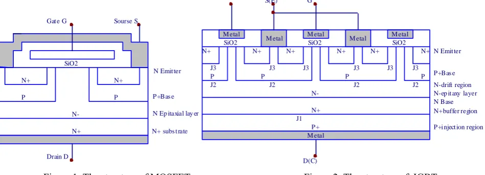
Basic Structure of MOSFET. Insulated Gate Field Effect Transistor (IGFET) uses SiO2 insulating layer between gate and source, gate and drain. The gate is made of aluminum metal and the gate resistance is over 1000 ohms. In order to fabricate high-power Metal Oxide Semiconductor FET (MOSFET), The substrates of N-channel enhanced insulated gate FET adopts N-type substrates with high doping N+ region. As shown in Figure 1. Low-doped N-region (N-type epitaxy layer) is epitaxied on N+ substrates, which together acts as the drain region and leads to drain D. The layer of P region is formed on the N-type epitaxy layer, and the highly doped N+ region is formed on the P region. From the overlooking of the P region and the N+ region, it can be seen that they are both annular regions, the N+ region is the source region, and the electrodes attached to it is the source S. The V-groove is formed by etching the middle to the N-type epitaxy layer. Because of the existence of the V-groove, the MOSFET is also named VMOS. The layer of insulating layer is grown on the V-groove and covered with a layer of metal (aluminum) that formed the control region of the device is called gate region, and the electrodes attached to it are called gate G. In this way, high power MOSFET is fabricated.
N+
N-N+
P
N+
P+Bas e Sourse S
Drain D Gat e G
N Emit ter
N Ep itaxial lay er
N+ subs t rate P
SiO2
N+
N-N+
P+
P+Bas e G
N Emit ter
N Base N+buffer region
P+i nject ion region P
J1
J2 J3
N+
J3 N+
D(C) P
J2 J3
N+
J3
N+ N+
P P
J2 J3
J2 J3 S(E)
M etal
SiO2 SiO2
M etal M etal
M etal M etal
M etal
SiO2
[image:3.595.61.536.467.638.2]N-ep it axy layer N-drift region
Figure 1. The structure of MOSFET. Figure 2. The structure of IGBT.
The additional base plate is the P+ layer drain injection region in Figure 2, and it is the unique functional region of IGBT. The N+ layer becomes the N+ layer buffer region between the P+ drain injection region and the N- epitaxy layer (N- drift region). The presence or absence of N+ layer buffer region determines the different characteristics of IGBT. The IGBT with N+ buffer region is called asymmetric IGBT, also known as through IGBT, which has the advantages of small forward voltage drop, short turn-off time and small tail current when turn-off, but its reverse blocking ability is relatively weak. The IGBT without N+ buffer region is called symmetric IGBT, also known as non-through IGBT, which has strong forward and backward blocking ability, but its other characteristics are not as good as asymmetric IGBT [2].
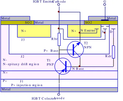
4-Layer PNPN Structure of IGBT. In the four-layer PNPN structure of IGBT, the P+ substrate constitutes a drain injection region. The metal layer and electrode attached to the P+ substrate are called the drain (collector C) of IGBT. The drain injection region P+ substrate is connected with the drain region. The drain region mainly consists of N+ layer buffer region and N-epitaxy layer. The equivalent structures of IGBT is combined by the MOSFET, triode PNP and NPN shown in Figure 3. P+ base and N base are defined. That is, the P region formed on the N-region is also called P+ base, and the N-region is also called N base or drift region. The layer of P region is formed on the N-type epitaxy layer, and a highly doped N+ region is formed on the P region. The P region here is also called the P+ base. The N+ region produced on the P region is the source region, and the N+ region is also called the N emitter. The electrodes attached to the N+ region are called the source (Emitter E) of IGBT. The control region of IGBT is still a gate region, and the electrode attached to it is a gate(G). IGBT can form conductive channel in the region close to the gate boundary, and the channel region formed in the P-type region between the drain region (N+ layer, N-layer) and the source region (N+ region) is the sub-channel region. Therefore, as can be seen from Figure 3 and Figure 4, a four-layer structure of P+N+N-PN+ of IGBT is formed from bottom to top.
M et al
M et al
M et al
N - ep i t ax y d ri ft reg io n
N +
P+ N
-P+ i n j ect io n reg io n
SO 2
N +
M et al
T1 PN P P+ B as e
T2 N PN R b r
S
R d r D C ath o d e
A n o d e
G
N E mi t ter
N B as e SO 2
N +
IGB T C o l ecto r IGB T Em i tt er
J 3
J 1 J 2
R b r
S
T2 N PN
M O SFE T
PN P
R d r D B
T1
G E
[image:4.595.70.534.314.613.2] [image:4.595.87.330.415.614.2]C
Figure 3. Four-Layer Structure of P+N+N-PN+ of IGBT. Figure 4. The Equivalent Circuit of IGBT.
PN Junction Formation and Transistor Equivalent Circuit in IGBT
PN Junction and Device Formation in IGBT
region with high doping concentration, forming the N+ emitter. The lower N region is the collector region with a large area and can withstand large current. The PNP structure is composed of P+ drain injection region, the drain region, and P+ base P region. The NPN structure is composed of the drain region, P+ base P region, and N+ source region. The MOSFET structure is composed of gate region, source region, conductive channel, sub-channel region and drain region. Therefore, the equivalent circuit of IGBT with parasitic transistor and MOSFET is shown in Figure 4. The IGBT of this structure is called N-channel IGBT (N-IGBT), similar to P-channel IGBT (P-IGBT), which is a
three-terminal device with gate G, collector C and emitter E. Rdr is N- Drift region equivalent
resistance. Rbr is the P+ Base region Equivalent Resistance and Distributed Resistance.
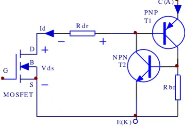
Modeling of IGBT Internal Thyristor
The PNP and NPN transistors in IGBT constitute a Thyristor (Silicon Controlled Rectifier, SCR) structure, as shown in Figure 5 and Figure 6. When positive high voltage is applied between anode A and cathode K and the control electrode TG is not applied, circuit A and K are high voltage blocking state. When positive high voltage is applied between anode A and cathode K with positive voltage between the control electrode TG and cathode K at the same time, conduction between anode A and
cathode K. The current of base B1 of PNP transistor is IB1(IB1). The current of collector C1 is
IC1(IC1) [1][3] :
B2 B1 1
C1 I I
I (2)
Where IC1 acts as the base current of NPN transistor. The current IB2(IB2) of base B2 of the NPN
transistor is1IB1.
The current IC2 (IC2) of collector C2 is
B1 1 1 B2 2
C2 I I
I (3) The amplification process mentioned above is carried out again to form the positive feedback. Therefore, in a short period of time, generally not more than a few microseconds, both PNP and NPN transistors are in the saturated state, thus the thyristor is fully turned on. Decreasing the current of anode A or changing the polarity of A-K voltage can achieve forward condition or reverse blocking.
As can be seen from Figure 6, the current of the thyristor control TG is Id.
B1 2 1 C2
B1
d I - I (1- )I
I (4)
Therefore, IGBT is the on-off of thyristor formed by the connection of PNP-NPN transistor controlled by MOSFET, that is, the voltage change of control TG of thyristor can be controlled by MOSFET, and the on-off between IGBT collector C and emitter E can be controlled by gate G based on MOSFET, so as to realize the control function of power supply.
R d r Id
M O SFE T
T1
G V d s
E(K )
C (A )
R b r T2
S D
B N PN
PN P
IB2 IC2
T2 T1
E(K )
C (A )
N PN PN P IB1
IC1
[image:5.595.119.310.619.753.2] [image:5.595.378.478.620.748.2]TG Id
Equivalent Circuit Analysis and Physical Modeling of IGBT
Equivalent Circuit Analysis of IGBT Physical Model
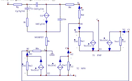
Based on the equivalent circuits of MOSFET, PNP and NPN, the micro-variable equivalent circuits of the three components of IGBT are established respectively as shown in the following Figure 7. The MOSFET has three working states of cut-off, amplifier and variable resistor. From Figure 3 and
Figure 7, the SCR is controlled by Id current, and the Id current is controlled by the voltage uGS. The
gate control signal uGS is generated by the motor controller. It is usually controlled by PWM square
wave with a certain driving power. The drain current Id should also reach a certain value [4].
2
GS(th) GS DO
d 1
u u I
I (5)
Where IDO is the Id value when uGS 2UGS(th).
When uDS 0 and uGS UGS(th) when the drain current Id 0, that is, the MOSFET is not on
and it works in the cut-off state.
When uDS 0 and uGS UGS(th), the drain current Id appears, that is, the MOSFET is on state.
When uDS uGS UGS(th), Id can be regarded as a controlled current source controlled by the
voltage uGS, that is, the MOSFET works in the amplification state.
When uDS uGS UGS(th) and uGS 2UGS(th), Id can be regarded as a saturated current, that is, the
MOSFET works in the saturated on state and in the variable resistance region. Therefore, IGBT uses
voltage uGS to control the cut-off state and saturated conduction state of MOSFET, and uses Id
controlled the SCR which is composed with PNP and NPN. So the IGBT can be realized turn off and
turn on by the gate voltage controlled uGS.
GND
NPN T1
Yre2Uc2
+ _
+ _
Yie2 B2
Yoe2
E1
Yfe2Ub2
Uc2
Ib2 Ic2
C1 Rg
G
Cds
S Ri
+
Cd(Ug,Ud)
Ud Ug Cg(Vg,Vd)
Id(U g,Ud)
Rs
Rd D
_
+
_
Yre1Uc1
+
_ +
_ Yie1 B1
Yoe1 C
Yfe1Ub1 Uc1
Ub1 Ib1
Ic1 Rdr
C2 Rbr
E Ub2
E2 M OSFET
T2
[image:6.595.77.504.457.720.2]PNP Id
Figure 7. The Micro-Variable Equivalent Circuits of The Three Components of IGBT.
The Parasitic Parameters and the Accurate Modeling and Analysis of IGBT
parameters include parasitic capacitance, parasitic inductance and junction resistance of voltage PN junctions, which are embodied in the transmission characteristics of IGBT. Therefore, through the simulation of the circuit, the equivalent parameters of the model of the actual components can be obtained while the best control transmission characteristics are obtained [5].
The 3D model of IGBT is built by Q3D and Simplorer simulation software in order to extract parasitic parameters. IBGT model based on micro-variable equivalent circuit is shown in the Figure 7.
The Rg, Rs and Rd are ohmic contact resistance of gate electrode, source electrode and drain
electrode respectively. Ri is resistance of semiconductor region between source and channel under
the positive gate. Cdsis drain source capacitance, mainly by metal. Capacitance determines the
constant. Cg and Cd are gate and channel capacitors, generally linear; Id is a voltage controlled drain
current source. Cg, Cd and Id are functions of internal gate voltage uGS and internal drain voltage
d
U or uDS [6][7].
Simplorer is used to simulate the transmission characteristics of IGBT, and the process of current
C
I changing with gate voltage uGS(VGE) at different temperatures is given. It can be seen in the Figure
9 that under different VGE(VM2,Vgin) conditions the simulation curves of AM1.1(IC) are obtained at
the environment temperature from 25C to 125C, which are basically consistent with those provided
by the IGBT user manual in Figure 8. By the modeling and parameters extraction methods can effectively extract the precise parameters of Rg, Rs, Rd, Ri, Rdr, Rbr, Cds, Cg, Cd , Yie1, Yie2, Yoe1
and Yoe2 etc. in the IGBT chip, so the corresponding distribution parameters can be determined and
the accurate model of IGBT chip can be achieved [8].
[image:7.595.330.506.400.760.2] [image:7.595.89.260.410.761.2]
Summary
IGBT is a composite fully controlled voltage-driven power semiconductor device composed of input stage MOSFET and output stage bipolar transistor PNP and NPN or GTR. When MOSFET is used for control and response, it has the characteristics of small driving power, fast switching speed, large input impedance, good thermal stability and simple driving circuit. The on-resistance of MOSFET increases rapidly with the increase of above 200 V or higher voltage, which makes its power consumption increase greatly that IGBT can’t obtain higher tolerance voltage and large capacity. BJT and GTR have the advantages of low on-voltage, low saturation voltage, high current density, high driving current, higher tolerance voltage, and are suitable for high-capacity power applications. However, they require large driving current, complex control circuits and insufficient switching speed. IGBT combines the advantages of these two devices. It has low driving power and low saturation voltage. Its frequency characteristics are between MOSFET and power transistor. Based on these excellent characteristics, IGBT adopts high frequency, high voltage and high current chip technology, which is widely used in voltage applications over 300V. Modular IGBT can meet higher current conduction requirements, and is very suitable for converter systems with DC voltage above 600V, such as AC motor, frequency converter, switching power supply, lighting circuit, traction drive and so on. At present, there are mainly international semiconductor manufacturers such as Infineon, ABB, Mitsubishi and so on. Among them, Infineon's N-IGBT module has the most obvious market advantage.
Acknowledgement
This research was financially supported by Research Foundation of General Equipment Department.
References
[1] Shi-bai Tong, Cheng-ying Hua, Fundamentals of Analog Electronics Technology[M], fourth ed., Higher Education Press, Beijing, 2011, pp. 12-43.
[2] Hai-hui Zha, Measurement of IGBT Power Device Parameters, China Integrated Circuit[J], 230 (2018), pp. 74-76.
[3] S. Iura, A. Narazaki, M. Inoue, S. Fujita, Development of New Generation 3.3 kV IGBT Module[J], Power Electronics. 42(9), 1998, pp. 76-78.
[4] Kai-yi Tang, Xin Yin, Zheng Shen, Zhi-kang Shuai, Gong Chen, Design Principles and Technical Comparisons of IGBT Gate Driver[J], Chinese Journal of Power Sources. 40(3), 2016, pp. 693-696.
[5] Li-wei Zhou, Ming-dan Zhang, Infineon new 34 mm Advantage series IGBT Modules and its application features and benefits in welding inverter[J], Electric Welding Machine, 46(8), 2016, pp. 67-70.
[6] Ming Chen, Design of Split Gate MOSFET with Graded-doped Drifting Region[J], Applications of IC, 35(5), 2018, pp. 35-37.
[7] Wei Hu, The Structure and Working Principle of IGBT[OL], 2019-03-28, http://m.elecfans. com/article/701446.html.