Phase separation during co-deposition of Al-Ge thin films
C. D. AdamsDepartment of Materials Science and Engineering, University of Michigan, Ann Arbor, Michigan 48109-2136
M. Atzmon
Department of Nuclear Engineering, University of Michigan, Ann Arbor, Michigan 48109-2104
Y-T. Cheng
Physical Chemistry Department, General Motors Research Laboratories, Warren, Michigan 48090-9055
D.J. Srolovitz
Department of Materials Science and Engineering, University of Michigan, Ann Arbor, Michigan 48109-2136
(Received 28 May 1991; accepted 30 October 1991)
We present the results of a combined experimental and theoretical investigation of phase separation and microstructure development in co-deposited A l - G e thin films. For small film thicknesses and deposition temperatures above 150 °C the phase-separated films consist of an array of domains of the Al- and Ge-rich terminal phases (lateral phase separation). Films deposited at 100 °C or less contained one or both of the terminal phases plus a metastable phase. We show that the domain structure evolves during deposition in a manner consistent with a surface interdiffusion controlled process. As film thickness increases we observe a transition from the laterally phase-separated microstructure to a layered microstructure exhibiting phase separation perpendicular to the film/substrate interface (transverse phase separation), with Al segregating to the film surface. We present a thermodynamic argument based on the competition between surface and interfacial free energies to explain this transition. Finally, we discuss the stability of the transverse phase-separated microstructure in the thick-film limit in terms of the transport of Ge through the Al-rich surface layer.
I. INTRODUCTION
Thin films are an integral part of most magnetic, optical, and electronic devices. Therefore, the properties of these films play a significant role in determining the ultimate performance capabilities of those devices. Numerous studies have shown that the physical and transport properties of thin films are strongly influ-enced by their microstructure. Thin film microstructure, in turn, is largely controlled by deposition conditions. Therefore, it is of great importance to understand the relationships between microstructure development and deposition conditions. One of the pioneering studies of these relationships was performed by Movchan and Demchishin over 20 years ago.1 These researchers iden-tified three distinct structural zones as a function of the homologous deposition temperature in which elemental metal and oxide thin films exhibited either a porous and "tapered" grain structure, a columnar grain structure, or a microstructure consisting of equiaxed grains. While there have been a number of studies of the influence of de-position conditions on the microstructure of multiphase films,2"6 there have been very few systematic studies and the effects of deposition conditions on multiphase film microstructure remain poorly understood.
One important aspect of multicomponent thin film deposition, which is unimportant during the deposition of elemental metal or oxide thin films, is phase sepa-ration. Depending upon the intended application, phase separation in a multicomponent thin film can be either desirable or undesirable, and is often an unexpected result of thin film processing. For example, in the case of multicomponent thin films used for magnetic recording media, the desired domain structure is the result of phase separation.7 However, in the case of compound semiconductors, such as In^GayAsi^Px^, phase separa-tion often occurs during processing and degrades device performance.8
C. D. Adams et al.: Phase separation during co-deposition of Al-Ge thin films
thin films during deposition. In film growth, however, the velocity of the reaction front is controlled by the externally imposed, finite, deposition rate. As a result, the microstructure of phase-separated films is strongly influenced by deposition conditions.
To address the question of phase separation in multi-component thin films, we have performed a combined experimental and theoretical study of phase separation in binary co-deposited A l - G e thin films as a function of film thickness and deposition temperature. The primary reason for selecting A l - G e as a model system for this study was its simple eutectic phase diagram with limited mutual solid solubilities.11 Therefore, phase separation into the terminal solid solutions is expected during co-deposition, provided that favorable kinetic conditions exist. Scanning and transmission electron microscopy were used to study the surface morphology, surface topography, and microstructure of the films. X-ray and electron diffraction were used for phase identification. Rutherford backscattering spectrometry, x-ray energy dispersive spectroscopy, Auger electron spectroscopy, and x-ray photoelectron spectroscopy were used for compositional analysis of the films.
Deposition conditions were such that we observed phase separation in all co-deposited A l - G e thin films studied as part of this investigation. At deposition tem-peratures above 150 °C the films consisted of only the Al- and Ge-rich terminal phases. Films deposited at temperatures below 150 °C contained one or both of the terminal phases in addition to a metastable phase. Films less than a critical thickness, determined by the deposition conditions, exhibited phase separation par-allel to the film/substrate interface (i.e., lateral phase separation). The domain size in these films increased with deposition temperature in an Arrhenius manner with an apparent activation energy of 0.19 eV/atom. This activation energy is consistent with surface interdiffu-sion controlled evolution of the film microstructure. As film thickness increases we observe a transition from a laterally phase-separated microstructure to a microstruc-ture phase-separated perpendicular to the film/substrate interface (i.e., transverse phase separation). A simple thermodynamic model is used to explain the origin of this transition.
II. EXPERIMENTAL PROCEDURE
A l - G e thin films, having a nominal composition of 40 at. % Ge, were co-deposited onto oxidized Si substrates by electron beam evaporation. The starting materials were 99.999% pure Al and Ge. Base pressure prior to deposition was less than 5 x 10"9 Torr (after source conditioning). Films 110 to 800 nm thick were deposited at substrate temperatures between 25 and 375 °C (see Table I). Substrate temperature was
mon-TABLE I. Matrix of the film thicknesses and deposition temperatures studied. Film Thickness 110 300 800 (nm) 25 X Deposition 70 100 X X temperature 150 X (°Q 200 XX X 375 X
itored with two chromel-alumel thermocouples mounted between the two substrate heaters at either end of the substrate. During deposition, substrate temperature rose by no more than 3 °C, except in the case of the 25 °C sample, where a 10 °C temperature rise was observed. The Al and Ge deposition rates were between 0.09 and 0.15 nm/s with deviations typically less than 0.03 nm/s. Hitachi S-520 and S-800 SEM's and a JEOL 2000FX TEM with a STEM attachment were used to study the phase morphology, surface topography, and micro-structure of the films. The x-ray energy dispersive spec-troscopy (XEDS) capabilities of the S-520 SEM and TEM were used to obtain compositional maps of the film microstructures. Electron and x-ray diffraction (in the Seemann-Bohlin thin film geometry) were used for phase identification. Plan-view and cross-sectional TEM specimens of selected samples were prepared by standard methods using a Gatan model 600 Dual Ion Mill with a liquid nitrogen cooled specimen stage. Surface topog-raphy of the films was investigated by first fracturing a film in liquid nitrogen to obtain a clean, brittle, fracture surface. These samples were then mounted for SEM examination such that the electron beam was incident at an angle of 10° relative to the film surface.
Rutherford backscattering spectrometry (RBS) and Auger electron spectroscopy (Perkin-Elmer Phi 600) were used to determine the overall composition and through-thickness homogeneity of the as-deposited films. X-ray photoelectron spectroscopy (Perkin-Elmer Phi 5400) combined with sputter depth profiling was also used to determine the near surface composition of selected films. Mechanically polished cross-sections of selected samples were prepared by gluing samples together film-to-film to study through-thickness homo-geneity using the XEDS capability of the SEM. Several films were also etched in a saturated NaOH solution to remove the Al-rich phase and allow the microstructure of the remaining Ge-rich film to be observed with SEM.
III. RESULTS
C. D. Adams ef a/.; Phase separation during co-deposition of Al-Ge thin films
varied considerably with deposition temperature and film thickness. We will consider the effects of these deposition parameters on microstructure development separately.
A. Deposition temperature effects
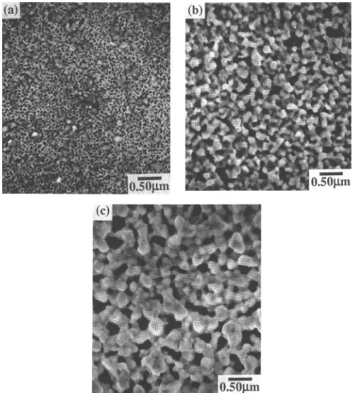
The SEM photomicrographs presented in Fig. 1 re-veal the effect of deposition temperature on the surface morphology of nominally 300 nm thick films deposited at temperatures of 25, 100, 150, 200, and 375 °C. The 375 °C film was somewhat thinner than the others, 200 nm instead of 300 nm. Figure 2 shows the surface topography of the same films as seen from glancing angle SEM images of fractured samples. Films deposited at 25 and 70 °C are characterized by a relatively smooth,
[image:3.576.296.524.272.658.2]O.SOfim
FIG. 1. Secondary electron SEM photomicrographs showing the ef-fect of deposition temperature on the surface morphology of films nominally 300 nm in thickness deposited at (a) 25 °C, (b) 100 °C, (c) 150 °C, (d) 200 °C, and (e) 375 °C. The film deposited at 375 °C was closer to 200 nm thick.
textured surface of uniformly sized features 20-50 nm in diameter [see Fig. l(a)]. In these samples, surface rough-ness is small compared to the total film thickrough-ness [see Fig. 2(a)]. Cross-sectional TEM of the film deposited at 25 °C shows that it consists of a fine, equiaxed, grain structure with a grain size much less than the film thickness and comparable to the scale of surface features. X-ray diffraction demonstrates that films deposited at 25 and 70 °C are a two-phase mixture of a micro-crystalline or amorphous phase and the face-centered cubic Al-rich terminal phase. A broad x-ray diffraction peak corresponding to the microcrystalline or amorphous
(a)
0.20jlm
0.25|im
[image:3.576.81.247.297.685.2]C D . Adams ef a/.: Phase separation during co-deposition of Al-Ge thin films
(C) (C)
. . . : : : : : : - •
• - "W.sa:s
.; • " " " »
.50|J-m
FIG. 1. (continued)
25|im
25\im
FIG. 2. (continued)
i citinn no - 77 3° films Using x-ray diffraction data from films deposited phase occurs at the same angular position (26/ - 21.5 nims. using A ia.y u „ _ , „„ . . «/. for Cu K« radiation) for both the 25 and 70 °C samples. at 25
[image:4.576.66.233.52.659.2] [image:4.576.253.511.62.668.2]C. D. Adams et al.: Phase separation during co-deposition of Al-Ge thin films
microcrystalline phase. As the Ge content was increased from 25 to 40 at. %, the integrated diffracted intensity from the face-centered cubic Al-rich terminal phase de-creased. A linear extrapolation to the A l - G e alloy com-position at which this diffracted intensity goes to zero provided an estimated composition for the amorphous or microcrystalline phase of 45 at. % Ge. It is interesting to note that this composition is within 10 at. % of the com-position obtained by extrapolation of the Al-rich liquidus to the deposition temperatures of 25 and 70 °C. Finally, due to the fine scale of the microstructures of these films, we were unable to correlate the phases observed by x-ray diffraction with specific features of the micro-structure observed in either SEM or TEM. However, based on the similarity of the microstructure of these films to that of other co-deposited A l - G e thin films,3 it appears that the microstructure consists of 20-50 nm grains of the Al-rich terminal phase embedded in an amorphous or microcrystalline matrix having a compo-sition of 45 at. % Ge.
X-ray diffraction showed that a film deposited at 100 °C is a three-phase mixture consisting of the Al-rich face-centered cubic and Ge-rich diamond cubic terminal phases and a third crystalline phase. From the positions of the lines in the x-ray diffraction pattern associated with this third phase we conclude that it is the monoclinic metastable Al7Ge3 phase previously observed by Larid-jani and Cahn12 and Koster13 in splat quenched A l - G e
alloy films and designated the 72 phase by Koster.13 The surface morphology depicted in the SEM photo-micrograph presented in Fig. l(b) was unique to the 300 nm thick films deposited at 100 °C. When viewed at normal incidence, the surface appears to have a wrinkled or cratered texture with features approximately 85 nm in diameter. The surface roughness of this sample represents only a small fraction of the film thickness [see Fig. 2(b)]. RBS analysis [see Fig. 3(a)] indicates that the film surface is enriched in Al relative to the bulk of the film, while near the substrate the film is enriched in Ge. The former is illustrated by the reduction in normalized yield, giving rise to a shoulder, on the high energy side of the Ge RBS signal and the small spike at the high energy side of the Al RBS signal. This is consistent with the composition of the film surface determined by XPS of 86 at. % Al, which is 3 1 % higher than the overall alloy composition of 55- at. % Al, as determined by RBS from the ratio of the integrated normalized yields for Al and Ge. The gradual decrease in normalized yield at the low energy side of the Al RBS signal in Fig. 3(a) indicates that the region of the film adjacent to the substrate is enriched in Ge. Removal of the Al-rich phase by etching the film in NaOH revealed a cellular microstructure of the underlying Ge enriched portion of the film adjacent to the substrate [see Fig. 4(a)]. This unusual cellular microstructure may be associated with
50 40 30 20 10 Energy (MeV)
0.4 0.6 0.8 1.0 1.2 1.4 1.6
0 100
i I I \
Temperature: 1 00°C
Thickness: 300nm
I I
Substrate
200 300 400 500 600 700 800
Channel
(a)
Energy (MeV)
0.4 0.6 0.8 1.0 1.2 1.4 -i 1—"—I r
Temperature: 1 50°C Thickness: 300nm 70 60 50 40 30 20
-10 - Substrate
1.6
— I —
100 200 300 400 500 Channel
600 700 800
(b)
FIG. 3. RBS spectra of 300 nm thick films deposited at (a) 100 °C and (b) 150 °C. The spectra show segregation of Al to the film surface and Ge to the film/substrate interface.
the formation of the metastable Al7Ge3 phase during deposition, as revealed by x-ray diffraction (see the preceding paragraph).
C. D. Adams et al.: Phase separation during co-deposition of Al-Ge thin films
(a)
[image:6.576.38.539.80.634.2]0.50iim
FIG. 4. Seconaary electron SHM photomicrographs of 300 nm thick films deposited at (a) 100 °C, (b) 150 °C, and (c) 200 °C after etching in NaOH to remove the Al-rich phase and expose the underlying Ge-rich phase.
the contrast observed in the SEM photomicrograph of Fig. l(c) to topographical contrast resulting from groov-ing at grain boundaries in the Al-rich phase. The Al-rich layer is visible in the SEM photomicrograph of the fracture surface shown in Fig. 2(c). Further evidence of
C D . Adams et al.: Phase separation during co-deposition of Al-Ge thin films
is 93 at. % Al, representing an enrichment of 39% above the overall film composition of 54 at. % Al determined by RBS. The presence of a shoulder on the low energy side of the Al RBS signal also indicates that near the substrate the film is enriched in Ge. The sponge-like microstructure of this Ge-rich layer, revealed after the Al-rich phase was removed by etching the film in NaOH, is depicted in the SEM photomicrograph presented in Fig. 4(b). Using XEDS in conjunction with SEM we find that there is a negligible amount of Al remaining in the film after etching. The faceting of the individual particles visible in Fig. 4(b) suggests that they are interconnected, single-crystal, grains of the Ge-rich phase, approximately 150 nm in diameter.
The surface morphology and topography of a 300 nm thick film deposited at 200 °C are shown in the SEM photomicrographs presented in Figs. l(d) and 2(d), re-spectively. The scale of the surface roughness of this film is larger than that of the lower temperature samples and is approximately 20% of the total film thickness. Similarly, the lateral dimension of the surface features has increased to approximately 700 nm. The results of TEM and SEM examination of a thinner film deposited at 200 °C, which will be discussed later, suggest that the bright, fine-structured material visible in Fig. l(d) is the Ge-rich phase while the smooth, and darker, areas of the photomicrograph correspond to Al-rich regions. Again, as in the case of the 300 nm thick film deposited at 150 °C, we attribute the contrast observed in the Al-rich regions of the film to topographical contrast arising from grooving at grain boundaries (see below). The film surface is nearly completely covered by a layer of the Al-rich terminal phase [see Fig. l(d)]. The Ge-rich phase is visible at the film surface, using SEM, only along grain boundaries and at holes in the Al-rich phase. Removal of this Al-rich layer by etching the film in NaOH revealed the sponge-like microstructure of the Ge-rich phase adjacent to the substrate [see Fig. 4(c)], which is similar to that observed in the 300 nm thick film deposited at 150 °C. In this case the grains of the Ge-rich phase are approximately 300 nm in diameter. SEM and XEDS again indicate that there is a negligible amount of Al remaining after etching.
The surface morphology and topography of a film deposited at 375 °C are shown in the SEM photomicro-graphs presented in Figs. l(e) and 2(e). As we indicated earlier, this film was somewhat thinner than the lower temperature films discussed thus far (200 nm instead of 300 nm). Unlike the 100, 150, and 200 °C films, there is no Al-rich layer covering the surface of this sample. Only phase separation parallel to the film/substrate interface is observed. XEDS, used in conjunction with SEM, shows that the darker regions in Fig. l(e) are Al-rich while the surrounding lighter, finely textured material, is Ge-rich. We will refer to the polycrystalline Al-rich regions as
Al domains and the polycrystalline Ge-rich region as Ge domains. The lateral dimension of the Al domains is approximately 700 nm [see Fig. l(e)]. Finally, the scale of the surface roughness of this film is of the same order as film thickness [see Fig. 2(e)] and the Ge domains rise only about half as far above the substrate as do the Al domains.
In summary, the co-deposited films phase separate during deposition into either a mixture of the Al- and Ge-rich terminal phases or a combination of one or both of the terminal phases and a metastable phase. The scale of the microstructure, both in terms of lateral di-mensions and surface roughness, increases as deposition temperature is increased.
B. Film thickness effects
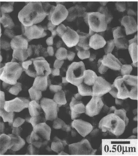
To investigate the effect of film thickness on the microstructures and surface morphologies of co-deposited A l - G e thin films, additional films were de-posited at 200 °C with thicknesses of 110 and 800 nm. The surface morphologies of these films, and that of a 300 nm thick film deposited at the same temperature, are shown in the SEM photomicrographs in Fig. 5. The 110 nm thick film [Fig. 5(a)] is characterized by phase separation into the Al- and Ge-rich terminal phases par-allel to the film/substrate interface (i.e., laterally phase-separated). However, closer SEM examination suggests the Al-rich phase is just beginning to cover the film surface at this deposition temperature and film thickness. At a film thickness of 300 nm [Fig. 5(b)] the surface is largely covered by a layer of the Al-rich phase. Finally, at a film thickness of 800 nm [Fig. 5(c)], the surface is completely covered by the Al-rich phase. An SEM photo-micrograph of a polished cross section of the 800 nm thick film (see Fig. 6) shows the extent of phase sepa-ration transverse to the substrate. The film is roughly divided into two halves: an Al-rich layer at the film surface and a Ge-rich layer adjacent to the substrate. Note, however, that the Al- and Ge-rich layers are not separated by a planar interface. Grains of the Ge-rich phase protrude into the rich overlayer and the Al-rich phase does contact the substrate at a few locations. Removal of the Al-rich phase by etching exposed the microstructure of the Ge-rich phase adjacent to the sub-strate (see Fig. 7). Two distinct ranges of grain sizes are evident. There appears to be a layer of small Ge-rich grains (~200 nm diameter) close to the substrate and an array of larger Ge-rich grains (~500 nm in diameter) above this layer (i.e., closer to the film surface).
C. D. Adams et al.: Phase separation during co-deposition of Al-Ge thin films
(a)!
(h)
[image:8.576.41.533.78.617.2](c)
FIG. 5. Secondary electron SEM photomicrographs showing the effect of film thickness on the surface morphology of films deposited at 200 °C having thicknesses of (a) 110 nm, (b) 300 nm, and (c) 800 nm. At 800 nm the film surface is entirely covered by a layer of the Al-rich phase (transverse phase separation).
the dark grey or black regions of the photomicrograph are predominantly Ge-rich, while the lighter regions are predominantly Al-rich. An exception is the large dark grain in the center of the photomicrograph which is Al-rich but oriented for strong diffraction. Note that the
C. D. Adams ef al.: Phase separation during co-deposition of Al-Ge thin films
[image:9.576.296.534.82.273.2]0.50jim
FIG. 6. Secondary electron SEM photomicrograph of a polished cross section through two samples of an 800 nm thick film deposited at 200 °C which shows the extent of transverse phase separation in this film. The cross section was prepared by epoxying two samples together film-to-film.
photomicrograph of Fig. 5(a), that the surface morphol-ogy (observed in SEM) of films showing only lateral phase separation is representative of the underlying bulk microstructure of the film. In our case, this applies to the 110 nm thick film deposited at 200 °C as well as the 200 nm thick film deposited at 375 °C. This result was also used earlier to interpret the SEM photomicrograph
,m
FIG. 7. Secondary electron SEM photomicrograph of an 800 nm thick film deposited at 200 °C after etching in NaOH to remove the Al-rich phase and reveal the Ge-rich phase. Two distinct ranges of grain sizes for the Ge-rich phase are evident: ~150 nm adjacent to the substrate and ~500 nm near the film surface.
[image:9.576.41.276.84.250.2]10.um
FIG. 8. Bright-field, plan-view, TEM photomicrograph of a 110 nm thick film deposited at 200 °C. The grain boundaries in the Al domains are in metastable equilibrium with respect to the grains of the Al domains (see arrows).
presented in Fig. l(d) of a 300 nm thick film deposited at 200 °C.
Finally, the uppermost arrow in Fig. 8 indicates the location of a triple junction in an Al domain at which the grain boundaries intersect at an angle of nearly 120°, indicative of equilibrium between grain boundaries of equal interfacial free energy. Similarly, Al grain boundaries are straight and traverse the Al domains at necks (see lower arrow in Fig. 8). We conclude from these observations that the Al grains and their boundaries are in metastable equilibrium for the size and shape the Al domains have achieved at 200 and 375 °C.
We have shown that as film thickness increases, for a fixed deposition temperature of 200 °C, we observe a transition from a laterally phase-separated microstructure to a microstructure exhibiting transverse phase separa-tion, with an Al-rich layer at the film surface. Except for the increase in the scale of the microstructure, an 800 nm thick film deposited at 200 °C has the same appearance as a 300 nm thick film deposited at 150 °C. Both films exhibit transverse phase separation. Finally, we have shown that the surface morphology of films exhibiting only lateral phase separation is representative of the underlying microstructure of the film.
IV. DISCUSSION
[image:9.576.41.279.415.684.2]C. D. Adams et al.: Phase separation during co-deposition of Al-Ge thin films
[image:10.576.297.537.97.253.2]when phase separation is expected from thermodynamic considerations, sluggish kinetics may preclude the for-mation of phase-separated microstructures consisting of the equilibrium phases. The kinetics established by our deposition conditions were such that we observed phase separation in all A l - G e films co-deposited at temper-atures between 25 and 375 °C. However, it was only for deposition temperatures of 150 °C or higher that the phase-separated films consisted of only the Al- and Ge-rich terminal phases. Films deposited at 100 °C also contained a monoclinic metastable phase in addition to the terminal phases. Films deposited at 25 and 70 °C contained the Al-rich terminal phase and an amorphous or microcrystalline phase containing 55 at. % Al.
TABLE II. Diffusion data for the Al-Ge system.
Diffusion mechanism Albulk self-diffusion Ge bulk self-diffusion Albulk
diffusion in Ge Ge bulk
diffusion in Al Ge surface
diffusion on Al
Activation energy (eV/atom) 1.26-1.31 2.95-3.1 3.27 1.26 0.52 Pre-exponential factor (m2/s) x KT4
0.11 10.8 214 0.48 Reference 14, 15 16, 17 18 15 19
A. Lateral phase separation
Films that were "thin" and/or deposited at elevated temperatures exhibited phase separation predominantly parallel to the film/substrate interface. As defined ear-lier, we refer to this as lateral phase separation. Phase separation perpendicular to the film/substrate interface is referred to as transverse phase separation. The meaning of the term "thin" depends on deposition temperature as illustrated by two films deposited at 200 and 375 °C, with thicknesses of 110 nm [see Fig. 5(a)] and 200 nm [see Fig. l(e)], respectively. The two films are laterally phase-separated. However, the thinner film deposited at 200 °C does show evidence of the Al-rich phase beginning to cover the film surface at the Ge domain boundaries. Therefore, at a film thickness of 110 nm and a deposition temperature of 200 °C we find evidence of the onset of transverse phase separation while at 375 °C a 200 nm thick film shows no evidence of transverse phase separation, whatsoever.
Throughout the deposition process there is a thermo-dynamic driving force for coarsening of the Al and Ge domains to minimize the contribution of A l - G e interfacial area to the total free energy of the system. Since such coarsening processes would occur through interdiffusion, kinetic limitations determine its extent. At low deposition temperatures, surface interdiffusion is the dominant kinetic process controlling coarsening and microstructure development. As deposition temper-ature is increased, the contribution of bulk diffusion to microstructure development is expected to become increasingly important. We now compare the relative contributions of surface and bulk diffusion.
Typical activation energies and pre-exponential fac-tors for various bulk and surface diffusion processes in the A l - G e system are presented in Table II. Using these values, the bulk diffusion coefficient for Al in Ge is 2.9 x 10~37 m2/s at 200 °C and that for bulk diffusion of Ge in Al is 1.8 x 10"18 m2/s at 200 °C. Assuming the bulk interdiffusion coefficient is the average of these two
values (9.0 x 10 19 m2/s), and setting the time spent at 200 °C during the deposition of a 110 nm thick film to 5 min, an interdiffusion distance [x = (Dt)112] of
16 nm is obtained. This interdiffusion distance is 5% of the domain diameter of ~300 nm we measured for a film of this thickness deposited at 200 °C. Therefore we conclude that bulk interdiffusion has a negligible influence on microstructure development of laterally phase-separated A l - G e films deposited at temperatures of 200 °C or less. For a 200 nm thick film deposited at 375 °C, the total time (deposition plus cooldown) spent above 200 °C was approximately 26 min. If we again use the average, temperature-dependent bulk interdiffu-sivity this leads to a bulk interdiffusion distance, dur-ing deposition and cooldown to 200 °C, of ~2000 nm, which is considerably larger than the domain diameter of 700 nm measured in this film. Therefore, we cannot rule out the possibility that bulk interdiffusion played a major role in the development of microstructure in the film deposited at this temperature. However, if the deep grooving [see Fig. 2(e)] observed at A l - G e interfaces of the film deposited at 375 °C was present throughout the deposition process, then it is highly plausible that this film lacked the bulk connectivity needed to sup-port a bulk interdiffusion process during deposition. We therefore conclude that the microstructural development of our co-deposited, laterally phase-separated, films was controlled by surface interdiffusion during the deposition process (at least for T ^ 200 °C). We demonstrate below that our experimental results are consistent with this interpretation.
C. D. Adams ef al.: Phase separation during co-deposition of Al-Ge thin films
in the reference frame that moves with the advancing surface, we find the following relation for the evolution of composition along the surface:
(1)
where Ds is the surface interdiffusivity of the two
elements and 6 is the width of the surface layer (of order the interatomic spacing). Equation (1) was originally derived by Cahn10 in his analysis of eutectoid growth and has since been rederived more generally elsewhere.20 In deriving Eq. (1) we assumed that the bulk diffusivity is negligible compared with the surface diffusivity. This implies that the composition profile in the film below the surface reflects the history of the composition profile at the film surface. In this picture, depth into the film is equivalent to time.
In order to apply this type of diffusional analysis to phase separation during film growth, we assume that a two-phase microstructure exists from the very earliest stages of deposition. The complex microstructure of the real film is idealized, as shown in Fig. 9, in order to make the problem more tractable. That is, we assume cylindrical a domains of radius R separated by a distance 21H by continuous regions of a second phase, /3, where 9K is equal to the radius of a circle of influence around each
a domain. In our situation, a represents the Al domains
and (3 the Ge domains. This idealized geometry is a good approximation when R -C 9t. The application of Eq. (1) to this geometry is discussed in detail by Atzmon et al.20 The natural scaling parameter for the length scale in this problem is p, which is the surface interdiffusion distance of Al and Ge in the time required to deposit a layer of thickness 6, given by:
[image:11.576.41.282.498.695.2]P = (2)
FIG. 9. Idealized domain structure of a laterally phase-separated film. The surface and interfacial free energies of interest are identified by the symbol, 7^, where x and y are a for the a phase, /3 for the /3 phase, v for the vapor, or s for the substrate.
The composition profile within an a domain, with the origin of the coordinate system at the domain center, is then given by:
and the composition profile outside the a domain is given by:
c\r) = (c° - c0)
°
where /„ and Kn are modified Bessel functions, of order n, of the first and second kind, respectively. c° and c°p
are the equilibrium compositions of the a and f3 phases, respectively, at the a-(3 interface, neglecting the effects of capillarity.
Mass balance yields the following equation:
(R/p)]Io(R/p)
[K
0(R/p)h(n/p)
^/p)]h{RI p)
or in the limit 91 ^> p:
KX{RIp)I0(R/p)
h(RI p)K0{R/p)
(5)
(6)
Consistent solutions are obtained when the left-hand side of Eq. (5) or (6) is sufficiently large, of the order of 3 or more. For c° « 1, c$ « 0, and IH/p ^ 4, Eq. (5) or (6) yields the following approximate values for R/p: 0.83 for c0 = 0.20, and 0.43 for c0 = 0.1. Therefore R is within a geometrical factor of p, the length scale associated with surface interdiffusion controlled coarsening. Using Eq. (2), R can be expressed as:
Roc (7)
This approach to determining R is very different from that taken by Cahn10 in his analysis of eutec-toid growth, where R was the euteceutec-toid plate size that minimizes the free energy of the system. Although experimental evidence supports Cahn's approach in sys-tems for which the velocity of the reaction front (v) is selected by the system,10 it has been shown that it is not applicable to systems in which v is an externally imposed variable,21'22 as in thin film deposition. In fact, we show, within the assumption of the present model,20 that the imposition of a fixed v is sufficient to determine R.
C. D. Adams et al.: Phase separation during co-deposition of Al-Ge thin films
sizes exhibit an Arrhenius temperature dependence with an apparent activation energy of 0.19 eV/atom. Equation (7) suggests that this activation energy should be 1/2 the activation energy of surface interdiffusion. Therefore, the activation energy for surface inter-diffusion is 0.38 eV/atom. It should be noted, however, that we cannot verify that the domain sizes in Fig. 10 have achieved their true, steady-state values, R. While correction of Fig. 10 to account for this may increase the apparent activation energy, this change is likely to be insignificant due to the logarithmic scale.
Table II presents several activation energies (usu-ally determined at high temperatures) reported in the literature for various types of diffusion in the A l - G e system. The activation energy determined using our data and Eq. (7) is much closer to that for surface diffusion than to any of the activation energies for bulk diffusion. Therefore, we conclude that the above theoretical analysis based on surface interdiffusion con-trolled microstructural evolution is consistent with our experimental data in the A l - G e system.
In summary, our experimental results on lateral phase separation in co-deposited Al—Ge thin films are consistent with an analysis in which the film phase sepa-rates into Al- and Ge-rich domains which coarsen by way of surface interdiffusion during deposition. Eventually the domain size reaches a steady-state value determined by the temperature-dependent surface interdiffusion dis-tance. The steady-state domain size exhibits an Arrhenius temperature dependence with an activation energy equal to half that for surface interdiffusion. Were it not for the onset of transverse phase separation, the films would
e
I
'a
S
©
a
es
1.0 2.0 3.0 4.0
[image:12.576.41.277.493.708.2]1000/TtK"
1]
FIG. 10. Domain sizes, determined from measurements on SEM photomicrographs plotted as a function of reciprocal temperature. The data exhibit Arrhenius behavior.
continue to thicken during deposition with the domain size remaining fixed at the steady-state value.
B. Transverse phase-separated films
As film thickness is increased from 110, to 300 and finally to 800 nm, at 200 °C, we observe a transition from a laterally phase-separated microstructure to one exhibiting transverse phase separation (see Fig. 5). The energetics of this transition can be analyzed in terms of the idealized microstructures shown in Figs. 9 and 11. In the laterally phase-separated microstructure (see Fig. 9), an increase in film thickness leads to an increase in the contribution of the A l - G e interfacial free energy to the total free energy of the system. However, in the case of a transverse phase-separated microstructure, the contribution of the interfacial free energy to the total free energy of the system remains constant, and independent of the film thickness, throughout deposition (see the idealized microstructure in Fig. 11). Therefore, we expect the laterally phase-separated microstructure to become unstable with respect to the transverse phase-separated microstructure for a sufficiently thick film.
With reference to Fig. 9, we can express the total interfacial free energy per unit film area associated with the laterally phase-separated microstructure as:
7lat = X{i<xv + las) + (1 - X){lpv + Ifis)
(8)
[image:12.576.296.539.564.713.2]where h, R, the surface and interfacial free energies (7's) are defined in the figure, and x — irR2/4£H2 is the volume fraction of the a phase (the Al-rich phase in our films). Due to the last term on the right side of Eq. (8), the energy of this microstructure increases with increas-ing film thickness and decreasincreas-ing phase domain size. The transverse phase-separated microstructure, depicted
C. D. Adams et al.: Phase separation during co-deposition of Al-Ge thin films
in Fig. 11, has the following total interfacial free energy per unit film area, independent of film thickness:
Ttrans = lav + la/3 + 7/3 s- (9) Without loss of generality in Eq. (9), we have labeled the phase in contact with the substrate in Fig. 11, /?. Note that 7trans is independent of the volume fraction of the
a phase.
The condition for the transition between the two types of phase-separated microstructures is obtained by equating Eqs. (8) and (9). This yields:
1 2a? 1 +
(1 - a;) x(yas
-lap
(10) For h/R < [h/R]c, the laterally phase-separated
micro-structure is stable, and for h/R > [h/R]c, transverse
phase separation is stable. Under certain conditions, the right-hand side of Eq. (10) can be negative, implying that the transverse phase-separated microstructure will be favored from the beginning of deposition.
The experimental results presented in Fig. 5 clearly show a transition from lateral to transverse phase separa-tion with increasing film thickness, in agreement with the predictions of Eq. (10). Although our study of the effect of film thickness on surface morphology and microstruc-ture was limited to a deposition temperamicrostruc-ture of 200 °C, experimental results and the model discussed above suggest the transition from a lateral to transverse phase-separated microstructure with increasing film thickness is a general result. For example, RBS analysis (see Fig. 3) and SEM examination [see Figs. l(c) and 2(c)] indicate that the surfaces of the 300 nm thick films deposited at 100 and 150 °C are enriched with Al relative to the overall film composition. Further, the theoretical analysis implies that the thickness at which this transition occurs increases with increasing domain size. Since the steady-state domain size increases with increasing deposition temperature [see Eq. (7) where there is a strong tem-perature dependence in Ds], this transition will occur at
larger thicknesses for higher temperatures. This result is consistent with our experimental observations where a 300 nm thick film shows complete surface Al coverage when deposited at 150 °C but not at 200 °C [compare Figs. l(c) and l(d)].
Clearly, the transverse phase-separated microstruc-ture cannot persist to very large film thicknesses since Ge must be transported from the advancing film surface to the Ge-rich layer, which is in contact with the substrate. Although bulk diffusion is very slow at these tempera-tures, significant Ge flux through the Al film may still be maintained due to grain boundary diffusion or via diffusion through holes in the Al film [see Fig. l(d)]. Nonetheless, at some point the Al layer thickness will
become sufficiently large that significant Ge supersatu-ration of the Al layer must occur. This supersatusupersatu-ration may be relieved by nucleation of Ge-rich domains within the Al-rich phase or by a Mullins-Sekerka23 instability of the A l - G e interface. This suggests a microstructure in which the surface is covered by the Al-rich phase, the substrate by the Ge-rich phase, and an equiaxed phase-separated region is present between them. We expect that the thickness of the Al- and Ge-rich layers will increase with increasing temperature due to the concomitant increase in diffusion length.24 This is supported by our RBS data, shown in Fig. 3, where a sample deposited at 150 °C has a thicker Al-rich layer than a sample of equal thickness deposited at 100 °C.
V. CONCLUSIONS
We observe phase separation in all A l - G e thin films co-deposited at temperatures between 25 and 375 °C. However, the form of the phase-separated microstruc-tures is strongly influenced by thermodynamics as well as kinetic factors determined by the deposition condi-tions. For deposition above 150 °C, films consist of the Al- and Ge-rich terminal phases expected from the phase diagram. Below this temperature the films consist of a mixture of one or both terminal phases with a metastable phase. Films that were thin and/or deposited at elevated temperatures exhibited only lateral phase separation. Surface roughness and the lateral scale of the microstructures increased with the deposition temperature. Surface roughness is the result of grooving, driven by the need to balance interfacial free energies at grain and phase boundaries. We show that the lateral scale of the microstructure of the phase-separated films exhibits Arrhenius temperature dependence with an ac-tivation energy half that for surface interdiffusion. This suggests an activation energy for surface interdiffusion of 0.38 eV/atom, which is consistent with measured values.
As film thickness increases, we observe a transi-tion from a laterally phase-separated microstructure to a transverse phase-separated microstructure with an Al layer at the film surface and Ge near the substrate. We show that this transition should be expected based on the minimization of the contribution of interfacial free ener-gies to the total free energy of a phase-separated film.
ACKNOWLEDGMENTS
C. D. Adams et al.: Phase separation during co-deposition of Al-Ge thin films
authors would like to thank Dr. D. Kessler for useful discussions and the referees for their valuable comments.
REFERENCES
1. B. A. Movchan and A. V. Demchishin, Phys. Met. Metallogr. 28, 83 (1969).
2. B. Cantor and R. W. Cahn, Acta Metall. 24, 845 (1976). 3. G. Deutscher, M. Rappaport, and Z. Ovadyahu, Solid State
Commun. 28, 593 (1978).
4. N. Saunders and A. P. Miodownik, J. Mater. Sci. 22, 629 (1987). 5. Z.H. Barber, Vacuum 41, 1102 (1990).
6. A. G. Dirks, J. J. van den Broek, and P. E. Wierenga, J. Appl. Phys. 55, 4248 (1984).
7. S. H. Liou and C. L. Chien, J. Appl. Phys. 63, 4240 (1988). 8. S. Mahajan and M. A. Shahid, in Advances in Materials,
Process-ing and Devices in III-V Compound Semiconductors, edited by D.K. Sadana, L. E. Eastman, and R. Dupuis (Mater. Res. Soc. Symp. Proc. 144, Pittsburgh, PA, 1989).
9. R. W. Cahn and P. Haasen, Physical Metallurgy (North-Holland, Amsterdam, 1983).
10. J.W. Cahn, Acta Metall. 7, 18 (1959).
11. Binary Alloy Phase Diagrams, edited by T. B. Massalski (ASM, Metals Park, OH, 1986), p. 116.
12. M. Laridjani and R. W. Cahn, Mater. Sci. Eng. 23, 125 (1976). 13. U. Koster, Z. Metallk. 63, 472 (1972).
14. T. E. Vollin and R. W. Balluffi, Phys. Status Solidi 25, 163 (1968). 15. N.L. Peterson and S.J. Rothman, Phys. Rev. B 1, 3264 (1970). 16. H. Widmer and G. R. Giinther-Mohr, Helv. Phys. Acta 34, 635
(1961).
17. H. Letaw, L. Slifkin, and W.M. Portnoy, Phys. Rev. 102, 636 (1956).
18. W. Meer and D. Pommerrenig, Z. Angew. Phys. 23, 369 (1967). 19. B. Ya Pines and Z.Z. Zyman, Fiz. Metal. Metalloved 25, 840
(1968).
20. M. Atzmon, D. A. Kessler, and D. J. Srolovitz (to be published). 21. D. A. Kessler and H. Levine, Phys. Rev. A 39, 3041 (1989). 22. T. Dombre and V. Hakim, Phys. Rev. A 36, 2811 (1987). 23. W.W. Mullins and R.F. Sekerka, J. Appl. Phys. 35, 444 (1964). 24. C. D. Adams, M. Atzmon, Y-T. Cheng, and D. J. Srolovitz, Appl.