2003 Microchip Technology Inc. May 2003 DS30277D
In-Circuit Serial Programming
™
DS30277D - page ii 2003 Microchip Technology Inc. Information contained in this publication regarding device
applications and the like is intended through suggestion only and may be superseded by updates. It is your responsibility to ensure that your application meets with your specifications. No representation or warranty is given and no liability is assumed by Microchip Technology Incorporated with respect to the accuracy or use of such information, or infringement of patents or other intellectual property rights arising from such use or otherwise. Use of Microchip’s products as critical com-ponents in life support systems is not authorized except with express written approval by Microchip. No licenses are con-veyed, implicitly or otherwise, under any intellectual property rights.
Trademarks
The Microchip name and logo, the Microchip logo, KEELOQ, MPLAB, PIC, PICmicro, PICSTART, PRO MATE and PowerSmart are registered trademarks of Microchip Technology Incorporated in the U.S.A. and other countries. FilterLab, microID, MXDEV, MXLAB, PICMASTER, SEEVAL and The Embedded Control Solutions Company are registered trademarks of Microchip Technology Incorporated in the U.S.A.
Accuron, Application Maestro, dsPIC, dsPICDEM, dsPICDEM.net, ECONOMONITOR, FanSense, FlexROM, fuzzyLAB, In-Circuit Serial Programming, ICSP, ICEPIC, microPort, Migratable Memory, MPASM, MPLIB, MPLINK, MPSIM, PICC, PICkit, PICDEM, PICDEM.net, PowerCal, PowerInfo, PowerMate, PowerTool, rfLAB, rfPIC, Select Mode, SmartSensor, SmartShunt, SmartTel and Total Endurance are trademarks of Microchip Technology Incorporated in the U.S.A. and other countries.
Serialized Quick Turn Programming (SQTP) is a service mark of Microchip Technology Incorporated in the U.S.A.
All other trademarks mentioned herein are property of their respective companies.
© 2003, Microchip Technology Incorporated, Printed in the U.S.A., All Rights Reserved.
Printed on recycled paper.
Microchip received QS-9000 quality system certification for its worldwide headquarters, design and wafer fabrication facilities in Chandler and Tempe, Arizona in July 1999 and Mountain View, California in March 2002. The Company’s quality system processes and procedures are QS-9000 compliant for its PICmicro®8-bit MCUs, KEELOQ®code hopping
devices, Serial EEPROMs, microperipherals, non-volatile memory and analog products. In addition, Microchip’s quality system for the design and manufacture of development systems is ISO 9001 certified.
Note the following details of the code protection feature on Microchip devices:
• Microchip products meet the specification contained in their particular Microchip Data Sheet.
• Microchip believes that its family of products is one of the most secure families of its kind on the market today, when used in the intended manner and under normal conditions.
• There are dishonest and possibly illegal methods used to breach the code protection feature. All of these methods, to our knowledge, require using the Microchip products in a manner outside the operating specifications contained in Microchip's Data Sheets. Most likely, the person doing so is engaged in theft of intellectual property.
• Microchip is willing to work with the customer who is concerned about the integrity of their code.
• Neither Microchip nor any other semiconductor manufacturer can guarantee the security of their code. Code protection does not mean that we are guaranteeing the product as “unbreakable.”
Code protection is constantly evolving. We at Microchip are committed to continuously improving the code protection features of our products. Attempts to break microchip’s code protection feature may be a violation of the Digital Millennium Copyright Act. If such acts allow unauthorized access to your software or other copyrighted work, you may have a right to sue for relief under that Act.
2003 Microchip Technology Inc. DS30277D-page iii
PAGE
SECTION 1INTRODUCTION
In-Circuit Serial Programming™ (ICSP™) Guide ... 1-1
SECTION 2
TECHNICAL BRIEFS
How to Implement ICSP™ Using PIC12C5XX OTP MCUs ... 2-1 How to Implement ICSP™ Using PIC16CXXX OTP MCUs ... 2-9 How to Implement ICSP™ Using PIC17CXXX OTP MCUs ... 2-15 How to Implement ICSP™ Using PIC16F8X FLASH MCUs ... 2-21
SECTION 3
PROGRAMMING SPECIFICATIONS
In-Circuit Serial Programming for PIC12C5XX OTP MCUs ... 3-1 In-Circuit Serial Programming for PIC12C67X and PIC12CE67X OTP MCUs ... 3-15 In-Circuit Serial Programming for PIC14000 OTP MCUs ... 3-27 In-Circuit Serial Programming for PIC16C55X OTP MCUs ... 3-39 Programming Specifications for PIC16C6XX/7XX/9XX OTP MCUs ... 3-51 In-Circuit Serial Programming for PIC17C7XX OTP MCUs ... 3-75 In-Circuit Serial Programming for PIC18CXXX OTP MCUs ... 3-101 PIC16F8X EEPROM Memory Programming Specification ... 3-147 PIC16F62X EEPROM Memory Programming Specification ... 3-161 PIC16F87X EEPROM Memory Programming Specification ... 3-181
SECTION 4
APPLICATION NOTES
In-Circuit Serial Programming™ (ICSP™) of Calibration Parameters
Using a PICmicro® Microcontroller ... 4-1
DS30277D-page iv © 2003 Microchip Technology Inc.
2003 Microchip Technology Inc. DS30277D-page 1-i
IN-CIRCUIT SERIAL
PROGRAMMING
™
GUIDE
Section 1 – Introduction
In-Circuit Serial Programming
™
Guide
=2003 Microchip Technology Inc. DS30277D-page 1-1
INTRODUCTION
WHAT IS IN-CIRCUIT SERIAL
PROGRAMMING (ICSP)?
In-System Programming (ISP) is a technique where a programmable device is programmed after the device is placed in a circuit board.
In-Circuit Serial Programming (ICSP) is an enhanced ISP technique implemented in Microchip’s PICmicro® One-Time-Programmable (OTP) and FLASH RISC microcontrollers (MCU). Use of only two I/O pins to serially input and output data makes ICSP easy to use and less intrusive on the normal operation of the MCU. Because they can accommodate rapid code changes in a manufacturing line, PICmicro OTP and FLASH MCUs offer tremendous flexibility, reduce development time and manufacturing cycles, and improve time to market.
In-Circuit Serial Programming enhances the flexibility of the PICmicro even further.
This In-Circuit Serial Programming Guide is designed to show you how you can use ICSP to get an edge over your competition. Microchip has helped its customers implement ICSP using PICmicro MCUs since 1992. Contact your local Microchip sales representative today for more information on implementing ICSP in your product.
PICmicro MCUs MAKE IN-CIRCUIT
SERIAL PROGRAMMING A CINCH
Unlike many other MCUs, most PICmicro MCUs offer a simple serial programming interface using only two I/O pins (plus power, ground and VPP). Following very sim-ple guidelines, these pins can be fully utilized as I/O pins during normal operation and programming pins during ICSP.
ICSP can be activated through a simple 5-pin connec-tor and a standard PICmicro programmer supporting Serial Programming mode such as Microchip’s PRO MATE® II.
No other MCU has a simpler and less intrusive Serial Programming mode to facilitate your ICSP needs.
WHAT CAN I DO WITH IN-CIRCUIT
SERIAL PROGRAMMING?
ICSP is truly an enabling technology that can be used in a variety of ways including:
• Reduce Cost of Field Upgrades
The cost of upgrading a system’s code can be dramatically reduced using ICSP. With very little effort and planning, a PICmicro OTP- or FLASH-based system can be designed to have code updates in the field.
For PICmicro FLASH devices, the entire code memory can be rewritten with new code. In PICmicro OTP devices, new code segments and parameter tables can be easily added in program memory areas left blank for update purpose. Often, only a portion of the code (such as a key algorithm) requires update.
• Reduce Time to Market
In instances where one product is programmed with different customer codes, generic systems can be built and inventoried ahead of time. Based on actual mix of customer orders, the PICmicro MCU can be programmed using ICSP, then tested and shipped. The lead-time reduction and simplification of finished goods inventory are key benefits.
• Calibrate Your System During Manufacturing
Many systems require calibration in the final stages of manufacturing and testing. Typically, calibration parameters are stored in Serial EEPROM devices. Using PICmicro MCUs, it is possible to save the additional system cost by programming the calibra-tion parameters directly into the program memory.
• Add Unique ID Code to Your System During Manufacturing
Many products require a unique ID number or a serial number. An example application would be a remote keyless entry device. Each transmitter has a unique “binary key” that makes it very easy to pro-gram in the access code at the very end of the man-ufacturing process and prior to final test.
Serial number, revision code, date code, manufac-turer ID and a variety of other useful information can also be added to any product for traceability. Using ICSP, you can eliminate the need for DIP switches or jumpers.
In-Circuit Serial Programming™ (ICSP™) Guide
Introduction
DS30277D-page 1-2 2003 Microchip Technology Inc.
In fact, this capability is so important to many of our customers that Microchip offers a factory program-ming service called Serialized Quick Turn Program-ming (SQTPSM), where each PICmicro MCU device is
coded with up to 16 bytes of unique code.
• Calibrate Your System in the Field
Calibration need not be done only in the factory. During installation of a system, ICSP can be used to further calibrate the system to actual operating environment.
In fact, recalibration can be easily done during periodic servicing and maintenance. In OTP parts, newer calibration data can be written to blank memory locations reserved for such use.
• Customize and Configure Your System in the Field
Like calibration, customization need not be done in the factory only. In many situations, customizing a product at installation time is very useful. A good example is home or car security systems where ID code, access code and other such information can be burned in after the actual configuration is deter-mined. Additionally, you can save the cost of DIP switches and jumpers, which are traditionally used.
• Program Dice When Using Chip-On-Board (COB)
If you are using COB, Microchip offers a comprehen-sive die program. You can get dice that are preprogrammed, or you may want to program the die once the circuit board is assembled. Programming and testing in one single step in the manufacturing process is simpler and more cost effective.
PROGRAMMING TIME
CONSIDERATIONS
Programming time can be significantly different between OTP and FLASH MCUs. OTP (EPROM) bytes typically program with pulses in the order of several hundred microseconds. FLASH, on the other hand, require several milliseconds or more per byte (or word) to program.
Figure 1 and Figure 2 below illustrate the programming time differences between OTP and FLASH MCUs. Figure 1 shows programming time in an ideal program-mer or tester, where the only time spent is actually pro-gramming the device. This is only important to illustrate the minimum time required to program such devices, where the programmer or the tester is fully optimized. Figure 2 is a more realistic programming time compar-ison, where the “overhead” time for programmer or a tester is built in. The programmer often requires 3 to 5 times the “theoretically” minimum programming time.
FIGURE 1: PROGRAMMING TIME FOR FLASH AND OTP MCUS
(THEORETICAL MINIMUM TIMES)
0 5 10 15 20 25 30 35 40 45
0 1K 2K 4K 8K 16K
Typical Flash MCU
Microchip OTP MCU
Programming T
ime (Seconds)
Note 1: The programming times shown here only include the total programming time for all memory. Typically, a programmer will have quite a bit of overhead over this “theoretical minimum” programming time.
2: In the PIC16CXX MCU (used here for comparison) each word is 14-bits wide. For the sake of simplicity, each word is viewed as “two bytes”.
Memory Size (in bytes) Typical FLASH MCU
Microchip OTP MCU
=2003 Microchip Technology Inc. DS30277D-page 1-3
Introduction
FIGURE 2: PROGRAMMING TIME FOR FLASH AND OTP MCUS
(TYPICAL PROGRAMMING TIMES ON A PROGRAMMER)
Ramifications
The programming time differences between FLASH and OTP MCUs are not particular material for prototyp-ing quantities. However, its impact can be significant in large volume production.
MICROCHIP PROVIDES A COMPLETE
SOLUTION FOR ICSP
Products
Microchip offers the broadest line of ICSP-capable MCUs:
• PIC12C5XX OTP, 8-pin Family • PIC12C67X OTP, 8-pin Family • PIC12CE67X OTP, 8-pin Family • PIC16C6XX OTP, Mid-Range Family • PIC17C7XX OTP High-End Family • PIC18CXXX OTP, High-End Family • PIC16F62X FLASH, Mid-Range Family • PIC16F8X FLASH, Mid-Range Family • PIC6F8XX FLASH, Mid-Range Family
All together, Microchip currently offers over 40 MCUs capable of ICSP.
Development Tools
Microchip offers a comprehensive set of development tools for ICSP that allow system engineers to quickly prototype, make code changes and get designs out the door faster than ever before.
PRO MATE II Production Programmer – a production quality programmer designed to support the Serial Programming mode in MCUs up to midvolume produc-tion. PRO MATE II runs under DOS in a Command Line mode, Microsoft® Windows® 3.1, Windows® 95/98, and Windows NT®. PRO MATE II is also capable of Serialized Quick Turn ProgrammingSM (SQTPSM), where each device can be programmed with up to 16 bytes of unique code.
Microchip offers an ICSP kit that can be used with the Universal Microchip Device Programmer, PRO MATE II. Together these two tools allow you to implement ICSP with minimal effort and use the ICSP capability of Microchip's PICmicro MCUs.
Technical support
Microchip has been delivering ICSP capable MCUs since 1992. Many of our customers are using ICSP capability in full production. Our field and factory appli-cation engineers can help you implement ICSP in your product.
Programming T
ime (Seconds)
Memory Size (in bytes)
Note 1: The programming times shown are actual programming times on vendor supplied programmers.
2: Microchip OTP programming times are based on PRO MATE II programmer. 0
20 40 60 80 100 120 140 160 180 200 220 240 260 280
0 1K 2K 4K 8K 16K
Typical Flash MCU
Microchip OTP MCU
Typical FLASH MCU
Microchip OTP MCU
Introduction
DS30277D-page 1-4 2003 Microchip Technology Inc.
2003 Microchip Technology Inc. DS30277D-page 2-i
IN-CIRCUIT SERIAL
PROGRAMMING
™
GUIDE
Section 2 – Technical Briefs
HOW TO IMPLEMENT ICSP™ USING PIC12C5XX OTP MCUS ... 2-1 HOW TO IMPLEMENT ICSP™ USING PIC16CXXX OTP MCUS ... 2-9 HOW TO IMPLEMENT ICSP™ USING PIC17CXXX OTP MCUS ... 2-15 HOW TO IMPLEMENT ICSP™ USING PIC16F8X FLASH MCUS ... 2-21
In-Circuit Serial Programming
™
Guide
=OMMP=jáÅêçÅÜáé=qÉÅÜåçäçÖó=fåÅK
Preliminary
apVNMNT_Jé~ÖÉ=OJNTB017
INTRODUCTION
The technical brief describes how to implement in-cir-cuit serial programming™ (ICSP) using the PIC12C5XX OTP PICmicro® MCU.
ICSP is a simple way to manufacture your board with an unprogrammed PICmicro MCU and program the device just before shipping the product. Programming the PIC12C5XX MCU in-circuit has many advantages for developing and manufacturing your product. • Reduces inventory of products with old
firmware. With ICSP, the user can manufacture product without programming the PICmicro MCU. The PICmicro MCU will be programmed just before the product is shipped.
• ICSP in production. New software revisions or additional software modules can be programmed during production into the PIC12C5XX MCU. • ICSP in the field. Even after your product has
been sold, a service man can update your program with new program modules.
• One hardware with different software. ICSP allows the user to have one hardware, whereas the PIC12C5XX MCU can be programmed with different types of software.
• Last minute programming. Last minute pro-gramming can also facilitate quick turnarounds on custom orders for your products.
IN-CIRCUIT SERIAL PROGRAMMING
To implement ICSP into an application, the user needs to consider three main components of an ICSP system: Application Circuit, Programmer and Programming Environment.
Application Circuit
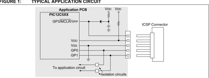
During the initial design phase of the application circuit, certain considerations have to be taken into account. Figure 1 shows and typical circuit that addresses the details to be considered during design. In order to implement ICSP on your application board you have to put the following issues into consideration:
1. Isolation of the GP3/MCLR/VPP pin from the rest of the circuit.
2. Isolation of pins GP1 and GP0 from the rest of the circuit.
3. Capacitance on each of the VDD, GP3/MCLR/ VPP, GP1, and GP0 pins.
4. Interface to the programmer.
5. Minimum and maximum operating voltage for VDD.
FIGURE 1: TYPICAL APPLICATION CIRCUIT
Author: Thomas Schmidt
Microchip Technology Inc.
Application PCB PIC12C5XX
GP3/MCLR/VPP
VDD
VSS
GP0 GP1
VDD VDD
To application circuit
Isolation circuits
ICSP Connector
How to Implement ICSP™ Using PIC12C5XX OTP MCUs
PICmicro, PRO MATE and PICSTART are registered trademarks of Microchip Technology Inc. In-Circuit Serial Programming and ICSP are trademarks of Microchip Technology Inc.
TB017
apVNMNT_Jé~ÖÉ=OJO
Preliminary
=OMMP=jáÅêçÅÜáé=qÉÅÜåçäçÖó=fåÅKIsolation of the GP3/MCLR/VPP Pin from the Rest of the Circuit
PIC12C5XX devices have two ways of configuring the MCLR pin:
• MCLR can be connected either to an external RC circuit or
• MCLR is tied internally to VDD
When GP3/MCLR/VPP pin is connected to an external RC circuit, the pull-up resistor is tied to VDD, and a capacitor is tied to ground. This circuit can affect the operation of ICSP depending on the size of the capac-itor.
Another point of consideration with the GP3/MCLR/VPP
pin, is that when the PICmicro MCU is programmed, this pin is driven up to 13V and also to ground. There-fore, the application circuit must be isolated from the voltage coming from the programmer.
When MCLR is tied internally to VDD, the user has only to consider that up to 13V are present during program-ming of the GP3/MCLR/VPP pin. This might affect other components connected to that pin.
For more information about configuring the GP3/ MCLR/VPP internally to VDD, please refer to the PIC12C5XX data sheet (DS40139).
Isolation of Pins GP1 and GP0 from the Rest of the Circuit
Pins GP1 and GP0 are used by the PICmicro MCU for serial programming. GP1 is the clock line and GP0 is the data line.
GP1 is driven by the programmer. GP0 is a bidirec-tional pin that is driven by the programmer when pro-gramming and driven by the PICmicro MCU when verifying. These pins must be isolated from the rest of the application circuit so as not to affect the signals dur-ing programmdur-ing. You must take into consideration the output impedance of the programmer when isolating GP1 and GP0 from the rest of the circuit. This isolation circuit must account for GP1 being an input on the PIC-micro MCU and for GP0 being bidirectional pin. For example, PRO MATE® II has an output impedance of 1 kW. If the design permits, these pins should not be used by the application. This is not the case with most designs. As a designer, you must consider what type of circuitry is connected to GP1 and GP0 and then make a decision on how to isolate these pins.
Total Capacitance on VDD, GP3/MCLR/VPP, GP1, and GP0
The total capacitance on the programming pins affects the rise rates of these signals as they are driven out of the programmer. Typical circuits use several hundred microfarads of capacitance on VDD, which helps to dampen noise and improve electromagnetic interfer-ence. However, this capacitance requires a fairly strong driver in the programmer to meet the rise rate timings for VDD.
Interface to the Programmer
Most programmers are designed to simply program the PICmicro MCU itself and don’t have strong enough drivers to power the application circuit.
One solution is to use a driver board between the pro-grammer and the application circuit. The driver board needs a separate power supply that is capable of driv-ing the VPP, VDD, GP1, and GP0 pins with the correct ramp rates and also should provide enough current to power-up the application circuit.
The cable length between the programmer and the cir-cuit is also an important factor for ICSP. If the cable between the programmer and the circuit is too long, signal reflections may occur. These reflections can momentarily cause up to twice the voltage at the end of the cable, that was sent from the programmer. This voltage can cause a latch-up. In this case, a termina-tion resistor has to be used at the end of the signal line.
Minimum and Maximum Operating Voltage for VDD
The PIC12C5XX programming specification states that the device should be programmed at 5V. Special con-siderations must be made if your application circuit operates at 3V only. These considerations may include totally isolating the PICmicro MCU during program-ming. The other point of consideration is that the device must be verified at minimum and maximum operation voltage of the circuit in order to ensure proper program-ming margin.
For example, a battery driven system may operate from three 1.5V cells giving an operating voltage range of 2.7V to 4.5V. The programmer must program the device at 5V and must verify the program memory con-tents at both 2.7V and 4.5V to ensure that proper pro-gramming margins have been achieved.
=OMMP=jáÅêçÅÜáé=qÉÅÜåçäçÖó=fåÅK
Preliminary
apVNMNT_Jé~ÖÉ=OJPTB017
THE PROGRAMMER
PIC12C5XX MCUs only use serial programming and, therefore, all programmers supporting these devices will support the ICSP. One issue with the programmer is the drive capability. As discussed before, it must be able to provide the specified rise rates on the ICSP sig-nals and also provide enough current to power the application circuit. It is recommended that you buffer the programming signals.
Another point of consideration for the programmer is what VDD levels are used to verify the memory contents of the PICmicro MCU. For instance, the PRO MATE II verifies program memory at the minimum and maxi-mum VDD levels for the specified device and is there-fore considered a production quality programmer. On the other hand, the PICSTART® Plus only verifies at 5V and is for prototyping use only. The PIC12C5XX pro-gramming specifications state that the program mem-ory contents should be verified at both the minimum and maximum VDD levels that the application circuit will be operating. This implies that the application circuit must be able to handle the varying VDD voltages. There are also several third-party programmers that are available. You should select a programmer based on the features it has and how it fits into your program-ming environment. The Microchip Development Sys-tems Ordering Guide (DS30177) provides detailed information on all our development tools. The Micro-chip Third Party Guide (DS00104) provides information on all of our third party development tool developers. Please consult these two references when selecting a programmer. Many options exist including serial or par-allel PC host connection, stand-alone operation, and single or gang programmers.
PROGRAMMING ENVIRONMENT
The programming environment will affect the type of programmer used, the programmer cable length, and the application circuit interface. Some programmers are well suited for a manual assembly line while others are desirable for an automated assembly line. A gang programmer should be chosen for programming multi-ple MCUs at one time. The physical distance between the programmer and the application circuit affects the load capacitance on each of the programming signals. This will directly affect the drive strength needed to pro-vide the correct signal rise rates and current. Finally, the application circuit interface to the programmer depends on the size constraints of the application cir-cuit itself and the assembly line. A simple header can be used to interface the application circuit to the pro-grammer. This might be more desirable for a manual assembly line where a technician plugs the programmer cable into the board.
A different method is the uses spring loaded test pins (often referred as pogo-pins). The application circuit has pads on the board for each of the programming sig-nals. Then there is a movable fixture that has pogo pins
in the same configuration as the pads on the board. The application circuit is moved into position and the fixture is moved such that the spring loaded test pins come into contact with the board. This method might be more suitable for an automated assembly line. After taking into consideration the issues with the application circuit, the programmer, and the program-ming environment, anyone can build a high quality, reliable manufacturing line based on ICSP.
OTHER BENEFITS
ICSP provides several other benefits such as calibra-tion and serializacalibra-tion. If program memory permits, it would be cheaper and more reliable to store calibration constants in program memory instead of using an external serial EEPROM.
Field Programming of PICmicro OTP MCUs
An OTP device is not normally capable of being repro-grammed, but the PICmicro MCU architecture gives you this flexibility provided the size of your firmware is less than half that of the desired device.
This method involves using jump tables for the reset and interrupt vectors. Example 1 shows the location of a main routine and the reset vector for the first time a device with 0.5K-words of program memory is pro-grammed. Example 2 shows the location of a second main routine and its reset vector for the second time the same device is programmed. You will notice that the GOTO Main that was previously at location 0x0002 is replaced with an NOP. An NOP is a program memory location with all the bits programmed as 0s. When the reset vector is executed, it will execute an NOP and then a GOTO Main1instruction to the new code.
TB017
apVNMNT_Jé~ÖÉ=OJQ
Preliminary
=OMMP=jáÅêçÅÜáé=qÉÅÜåçäçÖó=fåÅKEXAMPLE 1: LOCATION OF THE FIRST MAIN ROUTINE AND ITS INTERRUPT VECTOR
MOVLW XX MOVWF OSCAL
PROGRAM MEMORY
0X000
0X1FF
GOTO MAIN1 0X001
MAIN1 0X040
0X080
CALIBRATION VALUE RESET VECTOR
MAIN1 ROUTINE
UNPROGRAMMED
UNPROGRAMMED
=OMMP=jáÅêçÅÜáé=qÉÅÜåçäçÖó=fåÅK
Preliminary
apVNMNT_Jé~ÖÉ=OJRTB017
EXAMPLE 2: LOCATION OF THE SECOND MAIN ROUTINE AND IT INTERRUPT VECTOR
(AFTER SECOND PROGRAMMING)
MOVLW XX MOVWF OSCAL
PROGRAM MEMORY
0X000
0X1FF
NOP 0X001
MAIN1 0X040
0X080
CALIBRATION VALUE RESET VECTOR
MAIN1 ROUTINE GOTO MAIN2
MAIN2
MAIN2 ROUTINE 0X10E
0X136
UNPROGRAMMED
UNPROGRAMMED
0X002
TB017
apVNMNT_Jé~ÖÉ=OJS
Preliminary
=OMMP=jáÅêçÅÜáé=qÉÅÜåçäçÖó=fåÅKSince the program memory of the PIC12C5XX devices is organized in 256 x 12 word pages, placement of such information as look-up tables and CALL instructions must be taken into account. For further information, please refer to application note AN581, Implementing Long Calls and application note AN556, Implementing a Table Read.
CONCLUSION
Microchip Technology Inc. is committed to supporting your ICSP needs by providing you with our many years of experience and expertise in developing in-circuit system programming solutions. Anyone can create a reliable in-circuit system programming station by cou-pling our background with some forethought to the cir-cuit design and programmer selection issues previously mentioned. Your local Microchip representa-tive is available to answer any questions you have about the requirements for ICSP.
=OMMP=jáÅêçÅÜáé=qÉÅÜåçäçÖó=fåÅK
Preliminary
apVNMNT_Jé~ÖÉ=OJTTB017
APPENDIX A: SAMPLE DRIVER BOARD SCHEMATIC
R6 1
V
mm
_OUT
TO CIRCU
IT
3
2
1
4
1U1A TLE2144A R9 100 R9 100
V
CC
Q1 2N3906
R10 100
R2 33k
5
6
7
U1B
TLE2144A
V
``
V
CC
15V
EXTERNAL POWER SUPPLY
R12 100k
V
mm
_I
N
FROM PROGRAMMER C1 1NF D1 12.7V
Q2 2N2222 R13 5k Q3 2N3906 C3 0.1µ
F
V
aa
_OUT
R15 1
TO CIRCU
IT
C6 0.1µ
F
10
9
8
U1C TLE2144A
V
CC
R18 100 R17 100
Q4 2N2222 R22 5k
R19 100 C4 1NF D2 6.2V
V
aa
_IN
12
13
14
U1D
TLE2144A
R4 10k
R21 100k
FROM PROGRAMMER
GP1_IN GND_IN
GN
D_OU
T
FROM PROGRAMMER FROM PROGRAMMER
TO CIRCUIT
GP1_OUT
GP0_IN
FROM PROGRAMMER
TO CIRCUIT
GP0_OUT
TO CIRCUIT
Note:
The driver board design MUST be tested in the user's application to determine the ef
fect
s of the applications
circuit on the programming signals timing. Changes may be required if the application places a significant load on V
DD
, V
PP
, GP0 or GP1.
*see text in technical brief.
TB017
apVNMNT_Jé~ÖÉ=OJU
Preliminary
=OMMP=jáÅêçÅÜáé=qÉÅÜåçäçÖó=fåÅK=OMMP=jáÅêçÅÜáé=qÉÅÜåçäçÖó=fåÅK
Preliminary
apVNMNP_Jé~ÖÉ=OJVTB013
INTRODUCTION
In-Circuit Serial Programming™ (ICSP) is a great way to reduce your inventory overhead and time-to-market for your product. By assembling your product with a blank Microchip microcontroller (MCU), you can stock one design. When an order has been placed, these units can be programmed with the latest revision of firmware, tested, and shipped in a very short time. This method also reduces scrapped inventory due to old firmware revisions. This type of manufacturing system can also facilitate quick turnarounds on custom orders for your product.
Most people would think to use ICSP with PICmicro® OTP MCUs only on an assembly line where the device is programmed once. However, there is a method by which an OTP device can be programmed several times depending on the size of the firmware. This method, explained later, provides a way to field upgrade your firmware in a way similar to EEPROM- or Flash-based devices.
HOW DOES ICSP WORK?
Now that ICSP appeals to you, what steps do you take to implement it in your application? There are three main components of an ICSP system: Application Circuit, Programmer and Programming Environment.
Application Circuit
The application circuit must be designed to allow all the programming signals to be directly connected to the PICmicro MCU. Figure 1 shows a typical circuit that is a starting point for when designing with ICSP. The application must compensate for the following issues: 1. Isolation of the MCLR/VPP pin from the rest of
the circuit.
2. Isolation of pins RB6 and RB7 from the rest of the circuit.
3. Capacitance on each of the VDD, MCLR/VPP, RB6, and RB7 pins.
4. Minimum and maximum operating voltage for VDD.
5. PICmicro Oscillator.
6. Interface to the programmer.
The MCLR/VPP pin is normally connected to an RC cir-cuit. The pull-up resistor is tied to VDD and a capacitor is tied to ground. This circuit can affect the operation of ICSP depending on the size of the capacitor. It is, there-fore, recommended that the circuit in Figure 1 be used when an RC is connected to MCLR/VPP. The diode should be a Schottky-type device. Another issue with MCLR/VPP is that when the PICmicro MCU device is programmed, this pin is driven to approximately 13V and also to ground. Therefore, the application circuit must be isolated from this voltage provided by the programmer.
FIGURE 1: TYPICAL APPLICATION CIRCUIT
Author: Rodger Richey
Microchip Technology Inc.
Application PCB PIC16CXXX
MCLR/Vpp
Vdd Vss RB7 RB6
Vdd Vdd
To application circuit
Isolation circuits
ICSP Connector
TB013
apVNMNP_Jé~ÖÉ=OJNM
Preliminary
=OMMP=jáÅêçÅÜáé=qÉÅÜåçäçÖó=fåÅKPins RB6 and RB7 are used by the PICmicro MCU for serial programming. RB6 is the clock line and RB7 is the data line. RB6 is driven by the programmer. RB7 is a bidirectional pin that is driven by the programmer when programming, and driven by the PICmicro MCU when verifying. These pins must be isolated from the rest of the application circuit so as not to affect the sig-nals during programming. You must take into consider-ation the output impedance of the programmer when isolating RB6 and RB7 from the rest of the circuit. This isolation circuit must account for RB6 being an input on the PICmicro MCU, and for RB7 being bidirectional (can be driven by both the PICmicro MCU and the pro-grammer). For instance, PRO MATE® II has an output impedance of 1k¾. If the design permits, these pins should not be used by the application. This is not the case with most applications so it is recommended that the designer evaluate whether these signals need to be buffered. As a designer, you must consider what type of circuitry is connected to RB6 and RB7 and then make a decision on how to isolate these pins. Figure 1 does not show any circuitry to isolate RB6 and RB7 on the application circuit because this is very application dependent.
The total capacitance on the programming pins affects the rise rates of these signals as they are driven out of the programmer. Typical circuits use several hundred microfarads of capacitance on VDD which helps to dampen noise and ripple. However, this capacitance requires a fairly strong driver in the programmer to meet the rise rate timings for VDD. Most programmers are designed to simply program the PICmicro MCU itself and don’t have strong enough drivers to power the application circuit. One solution is to use a driver board between the programmer and the application circuit. The driver board requires a separate power supply that is capable of driving the VPP and VDD pins with the correct rise rates and should also provide enough cur-rent to power the application circuit. RB6 and RB7 are not buffered on this schematic but may require buffer-ing dependbuffer-ing upon the application. A sample driver board schematic is shown in Appendix A.
The Microchip programming specification states that the device should be programmed at 5V. Special con-siderations must be made if your application circuit operates at 3V only. These considerations may include totally isolating the PICmicro MCU during program-ming. The other issue is that the device must be veri-fied at the minimum and maximum voltages at which the application circuit will be operating. For instance, a battery operated system may operate from three 1.5V cells giving an operating voltage range of 2.7V to 4.5V.
The programmer must program the device at 5V and must verify the program memory contents at both 2.7V and 4.5V to ensure that proper programming margins have been achieved. This ensures the PICmicro MCU option over the voltage range of the system.
This final issue deals with the oscillator circuit on the application board. The voltage on MCLR/VPP must rise to the specified program mode entry voltage before the device executes any code. The crystal modes available on the PICmicro MCU are not affected by this issue because the Oscillator Start-up Timer waits for 1024 oscillations before any code is executed. However, RC oscillators do not require any startup time and, there-fore, the Oscillator Startup Timer is not used. The pro-grammer must drive MCLR/VPP to the program mode entry voltage before the RC oscillator toggles four times. If the RC oscillator toggles four or more times, the program counter will be incremented to some value X. Now when the device enters programming mode, the program counter will not be zero and the program-mer will start programming your code at an offset of X. There are several alternatives that can compensate for a slow rise rate on MCLR/VPP. The first method would be to not populate the R, program the device, and then insert the R. The other method would be to have the programming interface drive the OSC1 pin of the PICmicro MCU to ground while programming. This will prevent any oscillations from occurring during pro-gramming.
Now all that is left is how to connect the application cir-cuit to the programmer. This depends a lot on the programming environment and will be discussed in that section.
Programmer
The second consideration is the programmer. PIC16CXXX MCUs only use serial programming and therefore all programmers supporting these devices will support ICSP. One issue with the programmer is the drive capability. As discussed before, it must be able to provide the specified rise rates on the ICSP signals and also provide enough current to power the application circuit. Appendix A shows an example driver board. This driver schematic does not show any buffer cir-cuitry for RB6 and RB7. It is recommended that an evaluation be performed to determine if buffering is required. Another issue with the programmer is what VDD levels are used to verify the memory contents of the PICmicro MCU. For instance, the PRO MATE II ver-ifies program memory at the minimum and maximum VDD levels for the specified device and is therefore con-sidered a production quality programmer. On the other hand, the PICSTART® Plus only verifies at 5V and is for prototyping use only. The Microchip programming specifications state that the program memory contents should be verified at both the minimum and maximum VDD levels that the application circuit will be operating. This implies that the application circuit must be able to handle the varying VDD voltages.
Note: The driver board design MUST be tested in the user's application to determine the effects of the application circuit on the programming signals timing. Changes may be required if the application places a significant load on VDD, VPP, RB6 OR
=OMMP=jáÅêçÅÜáé=qÉÅÜåçäçÖó=fåÅK
Preliminary
apVNMNP_Jé~ÖÉ=OJNNTB013
There are also several third party programmers that are available. You should select a programmer based on the features it has and how it fits into your programming environment. The Microchip Development Systems Ordering Guide (DS30177) provides detailed informa-tion on all our development tools. The Microchip Third Party Guide (DS00104) provides information on all of our third party tool developers. Please consult these two references when selecting a programmer. Many options exist including serial or parallel PC host con-nection, stand-alone operation, and single or gang pro-grammers. Some of the third party developers include Advanced Transdata Corporation, BP Microsystems, Data I/O, Emulation Technology and Logical Devices.
Programming Environment
The programming environment will affect the type of programmer used, the programmer cable length, and the application circuit interface. Some programmers are well suited for a manual assembly line while others are desirable for an automated assembly line. You may want to choose a gang programmer to program multi-ple systems at a time.
The physical distance between the programmer and the application circuit affects the load capacitance on each of the programming signals. This will directly affect the drive strength needed to provide the correct signal rise rates and current. This programming cable must also be as short as possible and properly terminated and shielded, or the programming signals may be corrupted by ringing or noise.
Finally, the application circuit interface to the program-mer depends on the size constraints of the application circuit itself and the assembly line. A simple header can be used to interface the application circuit to the pro-grammer. This might be more desirable for a manual assembly line where a technician plugs the programmer cable into the board. A different method is the use of spring loaded test pins (commonly referred to as pogo pins). The application circuit has pads on the board for each of the programming signals. Then there is a fixture that has pogo pins in the same configuration as the pads on the board. The application circuit or fix-ture is moved into position such that the pogo pins come into contact with the board. This method might be more suitable for an automated assembly line. After taking into consideration the issues with the appli-cation circuit, the programmer, and the programming environment, anyone can build a high quality, reliable manufacturing line based on ICSP.
Other Benefits
ICSP provides other benefits, such as calibration and serialization. If program memory permits, it would be cheaper and more reliable to store calibration con-stants in program memory instead of using an external serial EEPROM. For example, your system has a ther-mistor which can vary from one system to another. Storing some calibration information in a table format allows the microcontroller to compensate in software for external component tolerances. System cost can be reduced without affecting the required performance of the system by using software calibration techniques. But how does this relate to ICSP? The PICmicro MCU has already been programmed with firmware that per-forms a calibration cycle. The calibration data is trans-ferred to a calibration fixture. When all calibration data has been transferred, the fixture places the PICmicro MCU in programming mode and programs the PICmicro MCU with the calibration data. Application note AN656, In-Circuit Serial Programming of Calibra-tion Parameters Using a PICmicro Microcontroller, shows exactly how to implement this type of calibration data programming.
The other benefit of ICSP is serialization. Each individ-ual system can be programmed with a unique or ran-dom serial number. One such application of a unique serial number would be for security systems. A typical system might use DIP switches to set the serial num-ber. Instead, this number can be burned into program memory, thus reducing the overall system cost and lowering the risk of tampering.
Field Programming of PICmicro OTP MCUs
An OTP device is not normally capable of being reprogrammed, but the PICmicro MCU architecture gives you this flexibility provided the size of your firm-ware is at least half that of the desired device and the device is not code protected. If your target device does not have enough program memory, Microchip provides a wide spectrum of devices from 0.5K to 8K program memory with the same set of peripheral features that will help meet the criteria.
The PIC16CXXX microcontrollers have two vectors, reset and interrupt, at locations 0x0000 and 0x0004. When the PICmicro MCU encounters a reset or inter-rupt condition, the code located at one of these two locations in program memory is executed. The first list-ing of Example 1 shows the code that is first pro-grammed into the PICmicro MCU. The second listing of Example 1 shows the code that is programmed into the PICmicro MCU for the second time.
TB013
apVNMNP_Jé~ÖÉ=OJNO
Preliminary
=OMMP=jáÅêçÅÜáé=qÉÅÜåçäçÖó=fåÅKEXAMPLE 1: PROGRAMMING CYCLE LISTING FILES
First Program Cycle Second Program Cycle
_________________________________________________________________________________________
Prog Opcode Assembly |Prog Opcode Assembly
Mem Instruction |Mem Instruction
---0000 2808 goto Main ;Main loop |0000 0000 nop
0001 3FFF <blank> ;at 0x0008 |0001 2860 goto Main ;Main now
0002 3FFF <blank> |0002 3FFF <blank> ;at 0x0060
0003 3FFF <blank> |0003 3FFF <blank>
0004 2848 goto ISR ;ISR at |0004 0000 nop
0005 3FFF <blank> ;0x0048 |0005 28A8 goto ISR ;ISR now at
0006 3FFF <blank> |0006 3FFF <blank> ;0x00A8
0007 3FFF <blank> |0007 3FFF <blank>
0008 1683 bsf STATUS,RP0 | 0008 1683 bsf STATUS,RP0
0009 3007 movlw 0x07 |0009 3007 movlw 0x07
000A 009F movwf ADCON1 |000A 009F movwf ADCON1
. | .
. | .
. | .
0048 1C0C btfss PIR1,RBIF | 0048 1C0C btfss PIR1,RBIF
0049 284E goto EndISR |0049 284E goto EndISR
004A 1806 btfsc PORTB,0 |004A 1806 btfsc PORTB,0
. | .
. | .
. | .
0060 3FFF <blank> |0060 1683 bsf STATUS,RP0
0061 3FFF <blank> |0061 3005 movlw 0x05
0062 3FFF <blank> |0062 009F movwf ADCON1
. | .
. | .
. | .
00A8 3FFF <blank> |00A8 1C0C btfss PIR1,RBIF
00A9 3FFF <blank> |00A9 28AE goto EndISR
00AA 3FFF <blank> |00AA 1806 btfsc PORTB,0
. | .
. | .
. | .
---=OMMP=jáÅêçÅÜáé=qÉÅÜåçäçÖó=fåÅK
Preliminary
apVNMNP_Jé~ÖÉ=OJNPTB013
The example shows that to program the PICmicro MCU a second time the memory location 0x0000, originally
goto Main (0x2808), is reprogrammed to all 0’s which
happens to be a nop instruction. This location cannot be reprogrammed to the new opcode (0x2860) because the bits that are 0’s cannot be reprogrammed to 1’s, only bits that are 1’s can be reprogrammed to 0’s. The next memory location 0x0001 was originally blank (all 1’s) and now becomes a goto Main
(0x2860). When a reset condition occurs, the PICmicro MCU executes the instruction at location 0x0000 which is the nop, a completely benign instruction, and then executes the goto Main to start the execution of code. The example also shows that all program memory loca-tions after 0x005A are blank in the original program so that the second time the PICmicro MCU is pro-grammed, the revised code can be programmed at these locations. The same descriptions can be given for the interrupt vector at location 0x0004.
This method changes slightly for PICmicro MCUs with >2K words of program memory. Each of the goto Main and goto ISR instructions are replaced by the following code segments due to paging on devices with >2K words of program memory.
movlw <page> movlw <page>
movwf PCLATH movwf PCLATH
goto Main goto ISR
Now your one time programmable PICmicro MCU is exhibiting more EEPROM- or Flash-like qualities.
CONCLUSION
Microchip Technology Inc. is committed to supporting your ICSP needs by providing you with our many years of experience and expertise in developing ICSP solutions. Anyone can create a reliable ICSP program-ming station by coupling our background with some forethought to the circuit design and programmer selection issues previously mentioned. Your local Microchip representative is available to answer any questions you have about the requirements for ICSP.
TB013
apVNMNP_Jé~ÖÉ=OJNQ
Preliminary
=OMMP=jáÅêçÅÜáé=qÉÅÜåçäçÖó=fåÅKAPPENDIX A: SAMPLE DRIVER BOARD SCHEMATIC
R6 1
V
mm
_OUT
TO CIRCUIT
3
2
1
4
1
U1A TLE2144A R9 100 R9 100
V
CC
Q1 2N3906
R10 100
R2 33k
5
6
7
U1B
TLE2144A
V
``
V
CC
15V
EXTERNAL POWER SUPPLY
R12 100k
V
mm
_IN
FROM PROGRAMMER C1 1NF D1 12.7V
Q2 2N2222 R13 5k Q3 2N3906 C3 0.1µ
F
V
aa
_OUT
R15 1
TO CIRCUIT
C6 0.1µ
F
10
9
8
U1C TLE2144A
V
CC
R18 100 R17 100
Q4 2N2222 R22 5k
R19 100 C4 1NF D2 6.2V
V
aa
_IN
12
13
14
U1D
TLE2144A
R4 10k
R21 100k
FROM PROGRAMMER
RB6_IN GND
_
IN
GN
D_OU
T
FROM PROGRAMMER FROM PROGRAMMER
TO CIRCUIT
RB6_OUT
RB7_IN
FROM PROGRAMMER
TO CIRCUIT
RB7_OUT
TO CIRCUIT
Note:
The driver board design MUST be tested in the user's application to determine the
ef
fect
s of the application
circuit on the programming
signals timing. Changes
may be required if the applic
ation places a significant
load on Vdd, Vpp, RB6 or RB7.
*see text in technical brief.
2003 Microchip Technology Inc.
Preliminary
DS91015B-page 2-15TB015
INTRODUCTION
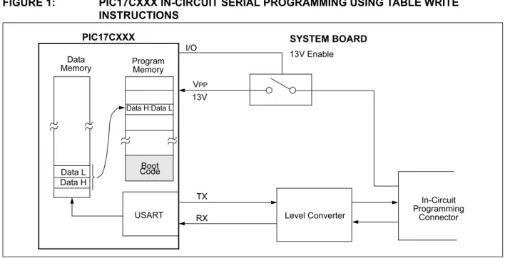
PIC17CXXX microcontroller (MCU) devices can be serially programmed using an RS-232 or equivalent serial interface. As shown in Figure 1, using just three pins, the PIC17CXXX can be connected to an external interface and programmed. In-Circuit Serial Program-ming (ICSP™) allows for a greater flexibility in an appli-cation as well as a faster time to market for the user's product.
This technical brief will demonstrate the practical aspects associated with ICSP using the PIC17CXXX. It will also demonstrate some key capabilities of OTP devices when used in conjunction with ICSP.
Implementation
The PIC17CXXX devices have special instructions, which enables the user to program and read the PIC17CXXX's program memory. The instructions are
TABLWT and TLWT which implement the program
mem-ory write operation and TABLRD and TLRD which per-form the program memory read operation. For more details, please check the In-Circuit Serial Programming for PIC17CXXX OTP Microcontrollers Specification
(DS30273), PIC17C4X data sheet (DS30412) and PIC17C75X data sheet (DS30264).
When doing ICSP, the PIC17CXXX runs a boot code, which configures the USART port and receives data serially through the RX line. This data is then pro-grammed at the address specified in the serial data string. A high voltage (about 13V) is required for the EPROM cell to get programmed, and this is usually supplied by the programming header as shown in Figure 1 and Figure 2. The PIC17CXXX's boot code enables and disables the high voltage line using a ded-icated I/O line.
FIGURE 1: PIC17CXXX IN-CIRCUIT SERIAL PROGRAMMING USING TABLE WRITE
INSTRUCTIONS Author: Stan D’Souza
Microchip Technology Inc.
PIC17CXXX Data
Memory ProgramMemory
Data L Data H
Boot Code
USART Level Converter
In-Circuit Programming
Connector I/O
13V Enable SYSTEM BOARD
VPP 13V
RX TX
Data H:Data L
How to Implement ICSP™ Using PIC17CXXX OTP MCUs
TB015
DS91015B-page 2-16
Preliminary
2003 Microchip Technology Inc.FIGURE 2: PIC17CXXX IN-CIRCUIT SERIAL PROGRAMMING SCHEMATIC
ICSP Boot Code
The boot code is normally programmed, into the PIC17CXX device using a PRO MATE® or PICSTART® Plus or any third party programmer. As depicted in the flowchart in Figure 4, on power-up, or a reset, the pro-gram execution always vectors to the boot code. The boot code is normally located at the bottom of the pro-gram memory space e.g. 0x700 for a PIC17C42A (Fig-ure 3).
Several methods could be used to reset the PIC17CXXX when the ICSP header is connected to the system board. The simplest method, as shown in Figure 2, is to derive the system 5V, from the 13V sup-plied by the ICSP header. It is quite common in manu-facturing lines, to have system boards programmed with only the boot code ready and available for testing, calibration or final programming. The ICSP header would thus supply the 13V to the system and this 13V would then be stepped down to supply the 5V required to power the system. Please note that the 13V supply should have enough drive capability to supply power to the system as well as maintain the programming volt-age of 13V.
The first action of the boot code (as shown in flowchart Figure 4) is to configure the USART to a known baud rate and transmit a request sequence to the ICSP host system. The host immediately responds with an acknowledgment of this request. The boot code then gets ready to receive ICSP data. The host starts send-ing the data and address byte sequences to the PIC17CXXX. On receiving the address and data information, the 16-bit address is loaded into the TBLPTR registers and the 16-bit data is loaded into the TABLAT registers. The RA2 pin is driven low to enable 13V at MCLR. The PIC17CXXX device then executes a table write instruction. This instruction in turn causes
a long write operation, which disables further code exe-cution. Code execution is resumed when an internal interrupt occurs. This delay ensures that the program-ming pulse width of 1 ms (max.) is met. Once a location is written, RA2 is driven high to disable further writes and a verify operation is done using the Table read instruction. If the result is good, an acknowledge is sent to the host. This process is repeated till all desired loca-tions are programmed.
In normal operation, when the ICSP header is not con-nected, the boot code would still execute and the PIC17CXXX would send out a request to the host. However it would not get a response from the host, so it would abort the boot code and start normal code execution.
FIGURE 3: BOOT CODE EXAMPLE
FOR PIC17C42A
PIC17CXXX
VDD
MCLR
RA2
RX VSS
+5V
MAX232 2N3905 13V
+5V
SERIAL PORT TX SERIAL PORT RX TX
7805
Programming Header
RESET Vector
Boot Code Program Memory
0x700
2003 Microchip Technology Inc.
Preliminary
DS91015B-page 2-17How to Implement ICSP™ Using PIC17CXXX OTP MCUs
FIGURE 4: FLOWCHART FOR ICSP BOOT CODE
Start
Received Host’s Configure USART and send request Goto Boot Code
Prepare to receive ICSP data
Do Table Write operation Received Address
and Data info?
Last Data/Address
Signal Programming Error
END
sequence? ACK?
Time-out complete?
Start Code Execution
Interrupt?
Read Program Location
Program location verified correctly?
No
Yes No
Yes
No
Yes
No
Yes
Yes No
Yes No
TB015
DS91015B-page 2-18
Preliminary
2003 Microchip Technology Inc.USING THE ICSP FEATURE ON
PIC17CXXX OTP DEVICES
The ICSP feature is a very powerful tool when used in conjunction with OTP devices.
Saving Calibration Information Using
ICSP
One key use of ICSP is to store calibration constants or parameters in program memory. It is quite common to interface a PIC17CXXX device to a sensor. Accurate, pre-calibrated sensors can be used, but they are more expensive and have long lead times. Un-calibrated sensors on the other hand are inexpensive and readily available. The only caveat is that these sensors have to be calibrated in the application. Once the calibration constants have been determined, they would be unique to a given system, so they have to be saved in program memory. These calibration parameters/constants can then be retrieved later during program execution and used to improve the accuracy of low cost un-calibrated sensors. ICSP thus offers a cost reduction path for the end user in the application.
Saving Field Calibration Information Using ICSP
Sensors typically tend to drift and lose calibration over time and usage. One expensive solution would be to replace the sensor with a new one. A more cost effec-tive solution however, is to re-calibrated the system and save the new calibration parameter/constants into the PIC17CXXX devices using ICSP. The user program however has to take into account certain issues: 1. Un-programmed or blank locations have to be
reserved at each calibration constant location in order to save new calibration parameters/con-stants.
2. The old calibration parameters/constants are all programmed to 0, so the user program will have to be "intelligent" and differentiate between blank (0xFFFF), zero (0x0000), and programmed locations. Figure 5 shows how this can be achieved.
Programming Unique Serial Numbers Using ICSP
There are applications where each system needs to have a unique and sometimes random serial number. Example: security devices. One common solution is to have a set of DIP switches which are then set to a unique value during final test. A more cost effective solution however would be to program unique serial numbers into the device using ICSP. The user applica-tion can thus eliminate the need for DIP switches and subsequently reduce the cost of the system.
FIGURE 5: FIELD CALIBRATION USING ICSP
Factory Settings Field Calibrate #1 Field Calibrate #2
Parameter 1.1 0xFFFF 0xFFFF 0xFFFF 0xFFFF 0xFFFF 0xFFFF Parameter 2.1
~
Parameter 1.3 0xFFFF
0xFFFF Parameter 2.3 Parameter 1.2
0xFFFF 0xFFFF
0xFFFF 0xFFFF Parameter 2.2
0x0000
0x0000
0x0000 0x0000
0x0000 0x0000
~
~~
~~
~~
~~
~~
~~
2003 Microchip Technology Inc.
Preliminary
DS91015B-page 2-19How to Implement ICSP™ Using PIC17CXXX OTP MCUs
Code Updates in the Field Using ICSP
With fast time to market it is not uncommon to see application programs which need to be updated or cor-rected for either enhancements or minor errors/bugs. If ROM parts were used, updates would be impossible and the product would either become outdated or recalled from the field. A more cost effective solution is to use OTP devices with ICSP and program them in the field with the new updates. Figure 6 shows an example where the user has allowed for one field update to his program.
Here are some of the issues which need to be addressed:
1. The user has to reserve sufficient blank memory to fit his updated code.
2. At least one blank location needs to be saved at the reset vector as well as for all the interrupts. 3. Program all the old "goto" locations (located at
the reset vector and the interrupts vectors) to 0 so that these instructions execute as NOPs. 4. Program new "goto" locations (at the reset
vec-tor and the interrupt vecvec-tors) just below the old "goto" locations.
5. Finally, program the new updated code in the blank memory space.
CONCLUSION
ICSP is a very powerful feature available on the PIC17CXXX devices. It offers tremendous design flex-ibility to the end user in terms of saving calibration con-stants and updating code in final production as well as in the field, thus helping the user design a low-cost and fast time-to-market product.
FIGURE 6: CODE UPDATES USING ICSP
Goto Boot
Production Program Code Update #1
Goto Boot
0x0000 0x0000
Main
Main1 Boot
Goto Main1 0xFFFF 0xFFFF
Goto Main
Main
Main1
Main2
Boot
0x0000 Goto Main2
0xFFFF
Goto Main
~ ~
~ ~
~ ~
~ ~
~ ~
~ ~
~ ~
~ ~
~ ~
~ ~
~ ~
~ ~
TB015
DS91015B-page 2-20
Preliminary
2003 Microchip Technology Inc.=OMMP=jáÅêçÅÜáé=qÉÅÜåçäçÖó=fåÅK apVNMNS_Jé~ÖÉ=OJON
TB016
INTRODUCTION
In-Circuit Serial Programming™ (ICSP) with PICmicro® FLASH microcontrollers (MCU) is not only a great way to reduce your inventory overhead and time-to-market for your product, but also to easily provide field upgrades of firmware. By assembling your product with a Microchip FLASH-based MCU, you can stock the shelf with one system. When an order has been placed, these units can be programmed with the latest revision of firmware, tested, and shipped in a very short time. This type of manufacturing system can also facil-itate quick turnarounds on custom orders for your prod-uct. You don’t have to worry about scrapped inventory because of the FLASH-based program memory. This gives you the advantage of upgrading the firmware at any time to fix those “features” that pop up from time to time.
HOW DOES ICSP WORK?
Now that ICSP appeals to you, what steps do you take to implement it in your application? There are three main components of an ICSP system.
These are the: Application Circuit, Programmer and Programming Environment.
Application Circuit
The application circuit must be designed to allow all the programming signals to be directly connected to the PICmicro MCUs. Figure 1 shows a typical circuit that is a starting point for when designing with ICSP. The application must compensate for the following issues: 1. Isolation of the MCLR/VPP pin from the rest of
the circuit.
2. Isolation of pins RB6 and RB7 from the rest of the circuit.
3. Capacitance on each of the VDD, MCLR/VPP, RB6, and RB7 pins.
4. Minimum and maximum operating voltage for VDD.
5. PICmicro Oscillator.
6. Interface to the programmer.
The MCLR/VPP pin is normally connected to an RC cir-cuit. The pull-up resistor is tied to VDD and a capacitor is tied to ground. This circuit can affect the operation of ICSP depending on the size of the capacitor. It is, there-fore, recommended that the circuit in Figure 1 be used when an RC is connected to MCLR/VPP. The diode should be a Schottky-type device. Another issue with MCLR/VPP is that when the PICmicro MCU device is programmed, this pin is driven to approximately 13V and also to ground. Therefore, the application circuit must be isolated from this voltage provided by the programmer.
FIGURE 1: TYPICAL APPLICATION CIRCUIT
Author: Rodger Richey
Microchip Technology Inc.
Application PCB PIC16F8X
MCLR/smm
Vdd Vss RB7 RB6
Vdd Vdd
To application circuit
Isolation circuits
ICSP Connector
How to Implement ICSP™ Using PIC16F8X FLASH MCUs
PICmicro, PRO MATE, and PICSTART are registered trademarks of Microchip Technology Inc. In-Circuit Serial Programming and ICSP are trademarks of Microchip Technology Inc.
TB016
apVNMNS_Jé~ÖÉ=OJOO =OMMP=jáÅêçÅÜáé=qÉÅÜåçäçÖó=fåÅK
Pins RB6 and RB7 are used by the PICmicro MCU for serial programming. RB6 is the clock line and RB7 is the data line. RB6 is driven by the programmer. RB7 is a bidirectional pin that is driven by the programmer when programming, and driven by the PICmicro MCU when verifying. These pins must be isolated from the rest of the application circuit so as not to affect the sig-nals during programming. You must take into consider-ation the output impedance of the programmer when isolating RB6 and RB7 from the rest of the circuit. This isolation circuit must account for RB6 being an input on the PICmicro MCU and for RB7 being bidirectional (can be driven by both the PICmicro MCU and the program-mer). For instance, PRO MATE® II has an output impedance of 1k¾. If the design permits, these pins should not be used by the application. This is not the case with most applications so it is recommended that the designer evaluate whether these signals need to be buffered. As a designer, you must consider what type of circuitry is connected to RB6 and RB7 and then make a decision on how to isolate these pins. Figure 1 does not show any circuitry to isolate RB6 and RB7 on the application circuit because this is very application dependent.
The total capacitance on the programming pins affects the rise rates of these signals as they are driven out of the programmer. Typical circuits use several hundred microfarads of capacitance on VDD which helps to dampen noise and ripple. However, this capacitance requires a fairly strong driver in the programmer to meet the rise rate timings for VDD. Most programmers are designed to simply program the PICmicro MCU itself and don’t have strong enough drivers to power the application circuit. One solution is to use a driver board between the programmer and the application circuit. The driver board requires a separate power supply that is capable of driving the VPP and VDD pins with the cor-rect rise rates and should also provide enough current to power the application circuit. RB6 and RB7 are not buffered on this schematic but may require buffering depending upon the application. A sample driver board schematic is shown in Appendix A.
The Microchip programming specification states that the device should be programmed at 5V. Special con-siderations must be made if your application circuit operates at 3V only. These considerations may include totally isolating the PICmicro MCU during program-ming. The other issue is that the device must be veri-fied at the minimum and maximum voltages at which the application circuit will be operating. For instance, a battery operated system may operate from three 1.5V
cells giving an operating voltage range of 2.7V to 4.5V. The programmer must program the device at 5V and must verify the program memory contents at both 2.7V and 4.5V to ensure that proper programming margins have been achieved. This ensures the PICmicro MCU option over the voltage range of the system.
This final issue deals with the oscillator circuit on the application board. The voltage on MCLR/VPP must rise to the specified program mode entry voltage before the device executes any code. The crystal modes available on the PICmicro MCU are not affected by this issue because the Oscillator Start-up Timer waits for 1024 oscillations before any code is executed. However, RC oscillators do not require any startup time and, there-fore, the Oscillator Startup Timer is not used. The pro-grammer must drive MCLR/VPP to the program mode entry voltage before the RC oscillator toggles four times. If the RC oscillator toggles four or more times, the program counter will be incremented to some value X. Now when the device enters programming mode, the program counter will not be zero and the program-mer will start programming your code at an offset of X. There are several alternatives that can compensate for a slow rise rate on MCLR/VPP. The first method would be to not populate the R, program the device, and then insert the R. The other method would be to have the programming interface drive the OSC1 pin of the PICmicro MCU to ground while programming. This will prevent any oscillations from occurring during pro-gramming.
Now all that is left is how to connect the application cir-cuit to the programmer. This depends a lot on the programming environment and will be discussed in that section.
Programmer
The second consideration is the programmer. PIC16F8X MCUs only use serial programming and therefore all programmers supporting these devices will support ICSP. One issue with the programmer is the drive capability. As discussed before, it must be able to provide the specified rise rates on the ICSP signals and also provide enough current to power the application circuit. Appendix A shows an example driver board. This driver schematic does not show any buffer cir-cuitry for RB6 and RB7. It is recommended that an evaluation be performed to determine if buffering is required. Another issue with the programmer is what VDD levels are used to verify the memory contents of the PICmicro MCU. For instance, the PRO MATE II ver-ifies program memory at the minimum and maximum VDD levels for the specified device and is therefore con-sidered a production quality programmer. On the other hand, the PICSTART® Plus only verifies at 5V and is for prototyping use only. The Microchip programming specifications state that the program memory contents should be verified at both the minimum and maximum VDD levels that the application circuit will be operating. This implies that the application circuit must be able to handle the varying VDD voltages.
Note: The driver board design MUST be tested in the user's application to determine the effects of the application circuit on the programming signals timing. Changes may be required if the application places a significant load on Vdd, VPP, RB6 or RB7.