MULTIPLE INPUT SINGLE OUTPUT CONVERTER WITH UNEVEN LOAD
SHARING CONTROL FOR IMPROVED SYSTEM EFFICIENCY
A Thesis
presented to
the Faculty of California Polytechnic State University,
San Luis Obispo
In Partial Fulfillment
of the Requirements for the Degree
Master of Science in Electrical Engineering
by
Kristen Yee-Shan Chan
ii © 2020
Kristen Yee-Shan Chan
iii
COMMITTEE MEMBERSHIP
TITLE: Multiple Input Single Output Converter with
Uneven Load Sharing Control for Improved
System Efficiency
AUTHOR: Kristen Yee-Shan Chan
DATE SUBMITTED: June 2020
COMMITTEE CHAIR: Taufik, Ph.D.
Professor of Electrical Engineering
COMMITTEE MEMBER: Majid Poshtan, Ph.D.
Associate Professor of Electrical Engineering
COMMITTEE MEMBER: Tina Smilkstein, Ph.D.
iv ABSTRACT
Multiple Input Single Output Converter with Uneven Load Sharing Control
for Improved System Efficiency
Kristen Yee-Shan Chan
This paper presents the development and study of multiple-input single-output
converter (MISO) for the DC House project that utilizes a controller to maximize the
overall converter’s efficiency. The premise of this thesis is to create uneven load current
sharing between the converters at different loading conditions in order to maximize the
efficiency of the overall MISO converter. The goal is to find a proper ratio of current
from each converter to the total load current of the MISO system to achieve the greatest
efficiency. The Arduino microcontroller is implemented to achieve this goal. The design
and operation of the MISO converter with the proposed controller will be explained in
this paper. The design and operation of the converter was tested and verified through
simulation in LTSpice in addition to hardware implementation. Different ratios of current
from each converter were used to fully test the MISO converter. For the 5A and 6A load
current, the maximum efficiencies were reached with the 70% / 30% ratio case, with
efficiencies of 94.91% and 95.07%, respectively. For 7A load current, the maximum
efficiency was reached with the 60% / 40% ratio case, with an efficiency of 94.59%. The
results were then compared with those obtained from the equal current sharing cases. For
the cases tested, the efficiency of the unequal current sharing outperforms that obtained
v
Keywords: Parallel, DC-DC Converter, Power Electronics, Buck, Multiple Input Single
vi
ACKNOWLEDGMENTS
First and foremost, I would like to thank Dr. Taufik for inspiring my interest in
power electronics. Your enthusiasm and immense knowledge in power electronics has
made me enjoy EE even more. You are one of the funniest, most down-to-earth, and
smartest professors that I know. Never stop telling your ghost and college stories to your
students! Those were some of the highlights of my days when I was in your power
electronics classes! Again, thank you so much for your guidance, patience, and
motivation in these past few years.
Thank you to Sabrinna Tan and Patricia Liu for coming into my life! You guys
helped me get through this tough year and I definitely wouldn’t have been able to do it
without our one bean cell that we share! Thanks for all the love and support y’all brought
into my life. Let’s continue our one-million-hour long Zoom calls forever, even when
Sab moves to Colorado! Also, don’t forget that we promised Hawaii!
Thank you to Kenny Nguyen, my thesis partner, who supported me immensely
throughout this past school year. Thanks for understanding the stress I felt throughout the
school year and being there for me. Also, thanks for being just a great person overall. I
can’t wait to see what you and your genius brain accomplish in the future.
Last but not least, I would like to thank the most important people in my life.
Thank you to my family: my dad, Chris, my mom, Jennet, my older sister, Jocelyn, and
my younger sister, Kaitlyn. I definitely would not be where I am today without you guys,
nor completed my thesis without your support and advice. Thank you guys for pushing
me, your encouragement, and ultimately, unconditional love, to help me achieve my
vii
TABLE OF CONTENTS
Page
LIST OF TABLES ... viii
LIST OF FIGURES ... ix
CHAPTER 1. INTRODUCTION ... 1
2. BACKGROUND ... 4
3. DESIGN REQUIREMENTS ... 11
4. DESIGN AND SIMULATION ... 14
5. HARDWARE DESIGN AND RESULTS ... 37
6. CONCLUSION ... 62
REFERENCES ... 65
APPENDICES A: ARDUINO CODE ... 69
B: SCHEMATIC ... 81
viii
LIST OF TABLES
Table Page
3-1: Summary of Design Requirements ... 13
5-1: Uneven Current Splitting and Efficiencies of Converter 1
with 5A Load Current... 48
5-2: Uneven Current Splitting and Efficiencies of Converter 2
with 5A Load Current... 49
5-3: Total Efficiencies with 5A Load Current ... 51
5-4: Uneven Current Splitting and Efficiencies of Converter 1
with 6A Load Current... 53
5-5: Uneven Current Splitting and Efficiencies of Converter 2
with 6A Load Current... 53
ix
LIST OF FIGURES
Figure Page
1-1: Number of smartphone users worldwide from 2016 to 2021 [1] ... 1
1-2: Functional block diagram of the DC House project [3] ... 2
2-1: Full bridge converter with phase shift pulse width modulation with two inputs [10] ... 7
2-2: Multiple input DC to DC soft-switching edge-resonant converter with two inputs [12-13] ... 8
3-1: Level 0 block diagram ... 11
3-2: Level 1 Block Diagram ... 12
4-1: Block diagram of stage 1, passthrough stage ... 14
4-2: Block diagram of stage 2, uneven current sharing ... 15
4-3: Voltage sense by a voltage divider ... 17
4-4: Zener diode as a voltage reference for the DAC... 22
4-5: MPX1D1264L220’s inductance value vs. current graph ... 23
4-6: Resistor divider on external pin of VFB ... 27
4-7: Circuit with two paralleled buck converters used to unevenly split current ... 28
4-8: Simulation of current splitting with 6A load current ... 30
4-9: Efficiency vs. percentage load current percentage with identical converters ... 31
4-10: Efficiency vs. percentage of 6A load current; one converter with DCR = 0.08Ω and one converter with no DCR ... 32
4-11: Efficiency vs percentage of 6A load current; one converter with DCR = 0.08Ω and one converter with DCR = 0.5Ω ... 33
x
5-1: Block diagram of stage 1, passthrough stage ... 37
5-2: Test setup of stage 1 ... 38
5-3: Part of Arduino code illustrating switch S1 off and switch S2 on. ... 39
5-4: Test results for switch S1 off and switch S2 on ... 39
5-5: Arduino code illustrating switch S1 on and switch S2 off ... 40
5-6: Test results for switch S1 on and switch S2 off ... 41
5-7: Stage 1 protoboard ... 41
5-8: Block diagram of stage 2, uneven current sharing ... 42
5-9: Schematic of LT3845 demo board, R8 and R9 highlighted ... 43
5-10: LT3845 demo board ... 43
5-11: Test configuration setup of stage 2 ... 45
5-12: Setup of entire circuit ... 45
5-13: Stage 2, demo boards in parallel with protoboard and Arduino ... 46
5-14: Stage 2 protoboard ... 46
5-15: Efficiency vs. Percentage load current with 5A load current ... 50
5-16: Overall efficiency vs. load current percentage of converter 1 with 5A load current ... 52
5-17: Efficiency vs. Percentage load current with 6A load current ... 54
5-18: Overall efficiency vs. load current percentage of converter 1 with 6A load current ... 55
5-19: Efficiency vs. Percentage load current with 7A load current ... 56
5-20: Overall efficiency vs. Percentage load current of converter 1 with 7A load current ... 57
xi
5-22: DAC values vs. Percentage load current of converter 1
with 5A load current ... 59
5-23: DAC values vs. load current percentage of converter 1
with 6A load current ... 59
5-24: DAC values vs. percentage load current of converter 1
1 1. INTRODUCTION
Since the development of electricity, Alternating Current (AC) has been the most
predominant form of electricity used in the world to transmit and distribute electrical
power from generating stations to loads. AC electricity offers advantages which make
them more preferred over the Direct Current (DC) counterpart. One major advantage
relates to the convenience in transforming AC voltage from one level to another level via
a transformer. This allows for efficient transmission of power from one location to
another resulting in a complete transformation of the power systems to AC. However,
with recent advances in power electronics it has become possible nowadays to perform
the same voltage transformation on DC voltages.
2
As electronics technology is advancing, the number of DC devices has been
increasing. Smartphone users worldwide for example has grown from 2.5 billion in 2016
to 3.3 billion in 2019, and is projected to continue to grow to 3.8 billion in 2021, as
shown in Figure 1-1 [1]. The continuing increase in DC devices poses a challenge for AC
electrical systems since this would imply the need for lossy AC to DC conversion or
rectifier. Coupled with the increasing DC energy sources such as solar panels and fuel
cells, interest in DC has returned.
Figure 1-2. Functional block diagram of the DC House project [3]
Several studies have investigated the use of a DC distribution system. In [2], a
small-localized DC distribution system for building loads is investigated. This power
system is supplied by a DC distributed energy source for the DC loads and has a separate
3
compared to a system solely based on AC through avoiding the use of the rectifier. In [3],
a residential DC electricity has been studied since 2010 at Cal Poly State University to
help provide access to electricity in rural, isolated, and remote areas mainly in developing
countries by utilizing small-scale renewable energy sources. The DC system is called the
DC House where several low power energy sources can be combined into a single DC
bus that powers a DC house, as depicted in Figure 1-2. The energy combiner plays an
important role in the DC House system and it is made up of stackable DC-DC converters
called the Multiple Input Single Output (MISO) converter. Since the inception of the DC
House project, several versions of the MISO converter have been developed with various
4 2. BACKGROUND
Throughout the world, people are gaining interest in DC electricity once again.
The fear that non-renewable fossil-based energy resources are being used up more
quickly than they can replace themselves is causing people to turn to renewable energy
sources. Additionally, people are looking into DC since converting from AC to DC
requires converters which will introduce significant loss [4]. As renewable energy
sources are becoming more attractive to power companies and consumers, the use of DC
is on the rise again mainly due to the more prevalent use of Photovoltaic (PV) which
produces DC electricity [5].
One research effort to utilize DC in everyday life is the DC House project
initiated in 2010 at Cal Poly State University [6]. The project aims to promote the use of
DC electricity using renewable energy to provide access to electricity in rural areas and
areas geographically difficult to be reached by power grid. Rural electrification can be
problematic, as distributing power from an AC grid can be expensive due to the need for
constructing facilities, transmission lines, and more. Therefore, the most feasible solution
for rural electrification is to produce electricity from their general surroundings. The
perfect sources for this would be renewable energy resources such as solar, wind, and
hydroelectric, which are usually plentiful in these areas [7]. With the exception of PVs
and fuel cells which produce DC, when small amount of power needed, the generators
used for the renewable energy sources commonly use DC electricity. This consequently
calls for the need to use DC to DC converter to convert and control the produced voltage
5
With the use of DC-DC converters to process the energy produced by renewable
energy sources, not only that the voltage matching between source and load can be
accomplished, but the DC-DC converters also increase the reliability and efficiency of
the overall system [8]. Equally important, the DC to DC conversion process is generally
very efficient and not as lossy as the AC to DC conversion. To date there are many types
of DC to DC converters, but in general they provide the step-down (buck), step-up
(boost), and up/down (buck-boost).
Because energy generation from renewable resources can vary from day to day
and even second to second, just as there could be a sudden loss of sunlight with cloud
cover coming in, a method to continuously pull in their energy is important. One method
to achieve this is by having multiple renewable energy sources to produce the electricity.
Within the DC House project, a DC-DC converter that has been developed to
accommodate multiple energy sources is called the Multiple Input Single Output (MISO)
converter. According to [9], there are four rules to determine whether a converter is
allowed to have multiple inputs. The first rule is that all input stages must have a forward
conducting bidirectional blocking switch, in which the common output stage must have
some control over the power delivered by each source. The next rule is that the
connection between the input stage and the common output stage should not have
independent controlled switches in parallel. The third rule is that both nodes of input
stage capacitor should not both be connected to the common output stage. Lastly, both
ends of the input source should not be terminals of the input stage, or else there will be a
6
In the end, it was determined that the two most feasible types of converters that can be
used as a multiple input converter include the boost and the buck-boost.
Outside of the DC House project, other researchers have proposed and explored
MISO converter topologies. One commonly known technical problem with MISO
converter is that when the input-stage circuits were put in parallel with a coupled
transformer in an interleaving method, the converter was only able to transfer energy
from one source to the load at a time. This will in turn produces several performance
issues including increased components’ stress, uneven thermal distribution, reduced
efficiency, and increased cost due to oversizing components in the converter.
One example of MISO converter was proposed by [10]. Figure 2-1 shows the
power stage of the converter. As shown, the converter utilizes the current-fed full-bridge
converter to address the aforementioned issue; however, it still has complications. It
employs a phase shift pulse width modulation technique, in which different power
sources are able to transfer into the load. This unfortunately presents switching losses, as
there are many power switches used in the topology. Increased complexity also comes in
the gating drivers and controller used, which makes the converter expensive and large in
7
Figure 2-1: Full bridge converter with phase shift pulse width modulation with two inputs
[10].
Another previous converter that has been proposed for renewable resources
solved these issues [11]. This converter is comprised of two current-fed input stage
circuits, a coupled transformer, and a bridge-rectifier, as shown in Figure 2-2. It was a
preferred converter at the time as it was simple, consisted of fewer components, a cheaper
alternative, and more efficient than the standard converter. However, the issue with this
converter for the MISO purpose is that it can only take two inputs, where ideally the
MISO converter should be able to take in as many inputs as the user wants.
Another previously explored solution addressed the issue with switching losses.
The MISO converter utilizes a soft-switching edge-resonant converter [12-13]. In
general, power losses can be present in a multiple input converter, especially in high
switching frequency, which will subsequently affect the efficiency. However, with a
zero-8
voltage switching and zero-current switching when the switch turns on. In this topology,
a maximum of 95.5% efficiency was observed.
Figure 2-2: Multiple input DC to DC soft-switching edge-resonant converter with two
inputs [12-13].
Within the DC House project, there have been multiple students designing
different MISO converters. One solution proposed a MISO full-bridge converter [14]. For
this converter, the primary side connects all of the sources together and the secondary
side combines the energy from the sources to the load. The biggest advantage of the
full-bridge converter is that there is only one single primary winding for each source, so there
are only three in total, since there are three renewable resources taken into consideration.
Consequently, the converter size will be smaller, since there will be a smaller winding
9
poor efficiency, never above 80%, and low total output power, around 80W. Another
MISO converter was proposed in [15] using the four-switch buck-boost converters and
implementing the peak current sharing controller for equal sharing of the sources. The
MISO converter was capable of achieving the equal current sharing technique by
designating the module with the largest load current as the master, in which all of the
other modules will either increase or decrease its own current to match the master’s
current. Unfortunately, there were still some issues with the proposed converter, namely
one MOSFET that appeared to be heating up more than others used in the circuit and
relatively poor line regulation of 3%.
Another student proposed and constructed another MISO converter that was
flexible, so it would work in different circumstances, not just specific cases [16]. This
design utilizes boost converters in order to eliminate the need for transformers, which
would introduce losses and decrease efficiency. This high-efficiency MISO converter
consists of multiple boost converters in parallel, in order to increase the amount of output
power. To prevent any back-feeding voltage, ORing diodes were placed at the outputs to
prevent any damage to other outputs. Because this converter incorporates current sharing,
the output voltages need to be regulated with great accuracy.
The latest MISO converter development from the DC House project resulted in a
US Patent where the converter possesses the desired characteristics of a true MISO
converter: scalable in power level, flexible to connect to as many sources, expandable
where more MISO modules could be added, equal load sharing, highly efficient, and
10
Despite the success in the MISO converter development, several further
improvements are in order. First, protection circuitry such as fusing and inversed polarity
must be added. Another improvement is the overall efficiency of the MISO converter at
any source and load conditions. Currently, the operation of the MISO converter forces the
MISO modules to equally share the load current. This, however, may not be the desired
operation since MISO module efficiency is a function of load. For example, at very low
load condition, it may be better to operate just one MISO connecting to one source,
instead of maintaining the equal load sharing.
To address the aforementioned issue with efficiency improvement of the MISO
converter at various loading conditions, this thesis aims to study and investigate the
proper mix of current contribution from each MISO module to the total load current
requirement to achieve the highest efficiency of the overall MISO converter. The MISO
converter will be designed, simulated, and constructed and its performance will be tested
and evaluated under unequal load sharing and then compared with those obtained from
11 3. DESIGN REQUIREMENTS
As stated in the previous chapter, the goal of this design is to maximize efficiency
of a MISO converter using unequal current sharing. This project will take in several
renewable energy sources and combine them into a single DC bus output. However, to
demonstrate the operation and functionality of the proposed method in maximizing the
efficiency while keeping the size and cost low, this project will utilize only two sources
as shown in Figure 3-1.
Figure 3-1: Level 0 block diagram.
The input sources will be chosen to come from renewable energy sources,
harvested from the sun, wind, water, or human power. From previous DC House projects,
in order to generate energy most efficiently, the nominal output voltage of the renewable
energy sources is 24V. This input voltage is allowed to vary from 12V to 60V. However,
in this thesis the nominal input voltage for the proposed MISO converter will have a
tolerance of +/- 6V to simplify the design. Given this, the input voltage will range from
12
In the previous DC House project, the single DC bus output was chosen to be 48
V due to many considerations such as cost, size, efficiency, etc. Therefore, with the 12V
to 60V input this would imply that the MISO topology must be a Buck-Boost. In this
thesis, the focus is on the method for automatic uneven current sharing to maximize
efficiency, and therefore the output voltage is chosen to be 12V to yield the simpler Buck
topology for the MISO converter.
Once constructed, the hardware prototype will undergo testing under different
loading conditions. This results in the output current of each buck converter to change
depending on the efficiency of the MISO. In particular, the MISO’s efficiency will be
maximized by automatically adjusting the currents from the converters with a
microcontroller. Each of the converters will be able to produce different amounts of
current to output a total of 3A. Therefore, the intended maximum output power for this
project is 36W. Figure 3-2 illustrates the level 1 block diagram of the MISO. A summary
of the technical specifications is shown in Table 3-1.
Figure 3-2: Level 1 Block Diagram. Buck
Converter 1 Microprocessor
Buck Converter 2
Microprocessor
Single Output 12V Renewable Energy
Source 1
13
Table 3-1: Summary of Design Requirements
Specification Value Justification
Nominal Input Voltage
24V 24V is the nominal output voltage coming from the renewable energy sources.
Input Voltage Tolerance
+/- 6V This range of input voltage (from 18V to 30V) will account for the renewable energy sources’ swings in voltages.
Nominal Output Voltage
12V As a proof of concept, the nominal output voltage will be 12V to allow the use of a step-down converter.
Output Current 3A This is selected to keep the size and cost of the overall system low.
14 4. DESIGN AND SIMULATION
The premise of this design is to maximize efficiency of the overall system. This
MISO converter will have different stages that will have their own purpose to contribute
to the overall goal. The first stage will implement diodes and switches to allow the
system to use either only one buck converter or to use two converters based on the overall
system’s efficiency. Figure 4-1 depicts this arrangement. In Chapter 3, it was stated that
the output load current would be 3A; however, the output current may need to be larger
to allow better test setup and measurements. The next stage, as shown in Figure 4-2, is
the paralleled buck converters that will implement uneven current sharing at different
loading conditions, from 5A to 7A, since all the components chosen for the two
converters are rated for 6A, as the demo boards used for the hardware test are rated at
6.25A each [18].
15
Figure 4-2: Block diagram of stage 2, uneven current sharing.
In the first stage, diodes are placed after the renewable energy sources or power
supplies to prevent any backflow of current feeding into any of the power supplies, and
switches that are controlled by a gate driver. The MOSFETs that are included in this
stage serve as switches to allow one or two converters to be operating at once, which is
determined by the efficiencies. There will be current and voltage sensors following the
two power supplies, which will be used to determine whether only one or two converters
will be connected to the load. The current and voltage sensors provide the needed
information for the microcontroller to calculate the input and output powers into the
converters, which in turn will determine which converters will be operated. If the sum of
the input power is low, then utilizing only one converter may potentially yield a more
efficient system. To make this decision, the microcontroller performs the comparison of
efficiencies of using one converter versus using two converters, and accordingly will
16
The second stage will unevenly split current under different loading conditions.
The buck converters will be used to decrease the input voltage down to 12V. This stage
will split the current unevenly between the two converters with current ratios of 10/90,
20/80, 30/70, 40/60, and 50/50, which will ultimately combine together again into one
single output. The uneven current between the two converters is achieved by injecting a
small voltage at the feedback pin of one of the buck converters. This small offset will
make the feedback voltage and output voltage of the converter respond accordingly. The
more voltage injected at the converter’s feedback pin, the more the current from the first
converter will decrease. As the small voltage offset at the feedback pin increases, the
output voltage decreases slightly, which in turn decreases the current. Then, the second
converter, with its feedback pin connected to ground, will output a current that
complements the current from the first converter to add up to the load current.
An Arduino will be used for the microcontroller, as it is cheap, readily available,
and convenient to use for this application. The Arduino will be incorporated with the
switches preceding the converters to help determine whether one or two converters will
be connected to the load. The current and voltage sensors are utilized to calculate input
power by the Arduino to the converters. The Arduino will then power the gate drivers on
and off to close and open the switches. In its default state, the path to using both
converters will be closed, so switch S1 will open and switch S2 will be closed, as implied
in Figure 4-1, allowing both converters to be used. When testing the efficiency for only
one converter, switch S1 will close and switch S2 will open. This causes the power from
the second renewable energy source to go through the path of switch S1 and into the first
17
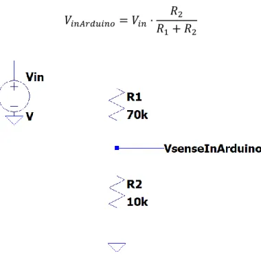
The voltage sense will be implemented using a resistor divider due to its
simplicity and ideal line regulation characteristic. Essentially, the resistor divider divides
the input voltage down by the divider ratio.
𝑉𝑖𝑛𝐴𝑟𝑑𝑢𝑖𝑛𝑜 = 𝑉𝑖𝑛⋅
𝑅2 𝑅1+ 𝑅2
Figure 4-3: Voltage sense by a voltage divider.
Thus, the input voltage will be multiplied by the ratio 𝑅2
𝑅1+𝑅2. For this project, the
chosen ratio is 1
8, as the input voltage can range from 18V to 30V. This results in the
reduced voltage into the Arduino which will range from 2.25V to 3.75V and is lower than
the 5V maximum input into analog pins. After the input voltage is divided by a certain
ratio, the output voltage of the resistor divider will be read into the Arduino. The Arduino
will then read that input analog voltage and multiply it by 8 to get an accurate voltage
from the input of the system. The resistor values 75kΩ and 11kΩ were then chosen to be
18
readily available. Therefore, that input analog voltage will be multiplied by 86
11 in the
Arduino.
Next, the INA169 will be used as the current sense amplifier. It works by
measuring the differential voltage across a small resistor value, thus converting the
current into a voltage. Then, the current will be calculated by the Arduino. In the INA169
datasheet [19], the following equation is used to find external resistors.
𝑉𝑜 =
𝐼𝑠⋅ 𝑅𝑠 ⋅ 𝑅𝐿 1𝑘𝛺
The output voltage of the current sense amplifier aims to be 5V since this is the
maximum input voltage of the Arduino. A value of 6A was chosen for Is as this is the
maximum current that the components of the converter are rated for. A small and
common value of 10mΩ was chosen for the sense resistor. Therefore:
5 =(6𝐴) ⋅ (10𝑚𝛺) ⋅ 𝑅𝐿 1𝑘𝛺
𝑅𝐿 = 83.33𝑘𝛺
With these measured voltages and currents, the Arduino can now calculate an
accurate input power. The final value used for the resistor was 82kΩ since it is a
commercially available nominal resistor value closest to the calculated resistor value.
Furthermore, the smaller resistor value also ensures that the 5V maximum limit of the
Arduino will not be exceeded. Then, 𝐼𝑆 can be found by rearranging the previous
19
𝐼
𝑠=
𝑉𝑜 ⋅ 1𝑘𝛺 𝑅𝑠 ⋅ 𝑅𝐿
,
where 𝑅𝐿 = 83.33𝑘𝛺, 𝑅𝑆 = 10𝑚𝛺, and 𝑉𝑜 is the analog input voltage to the Arduino.
Therefore,
𝐼𝑠 = 𝑉𝑜⋅50 41
After reading the analog input voltage into the Arduino, the current will be calculated by
multiplying the analog input voltage by the ratio 50
41.
Another component is the gate driver. This is the component that will be used to
enable the MOSFETs to pass or block the voltages. The gate driver that will be used is
the LTC7001 [20]. It was chosen due to its high input voltage input capability, up to
135V. Even though the gate driver’s input voltage may be higher than necessary, the
wide input voltage is useful to protect from for any transient swings or spikes from input
voltage without using additional protection device. The Arduino will provide 0V to 5V
pulses to the gate driver’s INP pin that will turn on and off the MOSFET. The gate driver
uses a bootstrap diode and capacitor to charge up to a voltage greater than the 24V input
connected to the gate of the MOSFET, which allows the MOSFET to turn on. This
process is applied to both S1 and S2.
The high voltage N-channel MOSFET [21] used as the switch to block or pass the
power from the renewable energy sources to the converters has a few main factors to
consider when sizing it. This includes the maximum voltage and average current. Based
on the circuit, the MOSFET should be able to handle a maximum voltage of 30V to
20
MOSFET AO4484 from Alpha and Omega Semiconductor matched all the specifications
and was therefore chosen for this project. The MOSFET has its maximum voltage at 40V,
the maximum drain current rating of 10A, and steady-state maximum junction-to-ambient
of 75°C/W.
Additionally, the Arduino will be programmed by the user to inject voltage at the
feedback pin of the first converter. Because 0.1mV resolution is desired, a high precision
digital to analog converter (DAC) must be used. The Arduino will be used to power the
DAC. The DAC8801 from Texas Instruments [22] has a serial peripheral interface (SPI)
protocol that will be used in this operation. It is also a 14-bit DAC, which will provide
enough resolution for the injected voltage as calculated below. The reference voltage Vref
chosen was 1.8V so that the voltage step would be small enough for the resolution that is
desired, which is in the 0.1mV range.
𝑉𝑠𝑡𝑒𝑝 =𝑉𝑟𝑒𝑓
214, where Vref = 1.8V
𝑉𝑠𝑡𝑒𝑝 =
1.8𝑉
16384= 0.11 𝑚𝑉
Because the desired resolution is so small, the DAC chosen needed to have
extremely little noise, as any noise can disrupt the operation of the system. The DAC’s
differential nonlinearity (DNL), which is the variation between two analog values
corresponding to its respective digital values, must be considered. The DAC8801’s
maximum DNL value is ±0.5, which means for one digital value, its corresponding
analog value can swing ±0.055𝑚𝑉 of its corresponding analog value.
21
Therefore, the injected voltage with a swing of ±0.055𝑚𝑉 will correspond to one
digital value. This resolution from this DAC meets the desired resolution.
Moreover, since the DAC’s reference voltage Vref is 1.8V, a Zener diode is used
to bring 5V down to 1.8V. From the datasheet, the DAC’s reference pin has an input
resistance of 5k𝛺. Therefore, as shown in the following equation, it requires about
360𝜇A.
𝐼𝑟𝑒𝑓 = 𝑉𝑟𝑒𝑓 𝑅𝑟𝑒𝑓 =
1.8𝑉
5𝑘𝛺 = 360𝜇𝐴
To allow extra current in case of any spikes on the reference pin, the reference pin
current was increased to 410𝜇A.
For the Zener diode, the MMSZ4678T1G was selected whose reverse voltage is
1.8V. In the datasheet [23], the reverse current of this specific diode is 50𝜇A. A value of
6.8k𝛺 was chosen for the resistor since it is a 5% standard value. Therefore, 60𝜇A will be
the expected reverse current through the Zener diode, which is similar to the datasheet’s
specified reverse current with a 10𝜇A leeway. The value of the resistance is calculated in
the following equation.
𝑅 = 𝑉𝑅 𝐼𝑅 =
𝑉𝐷𝐷−𝑉𝑟𝑒𝑓 410𝜇𝐴 + 60𝜇𝐴=
5𝑉−1.8𝑉
470𝜇𝐴 = 6.8𝑘𝛺.
A capacitor value of 0.1𝜇F was chosen since it is a standard value that is easily
accessible. The capacitor in parallel with the resistor and Zener diode is used to stabilize
22
Figure 4-4: Zener diode as a voltage reference for the DAC.
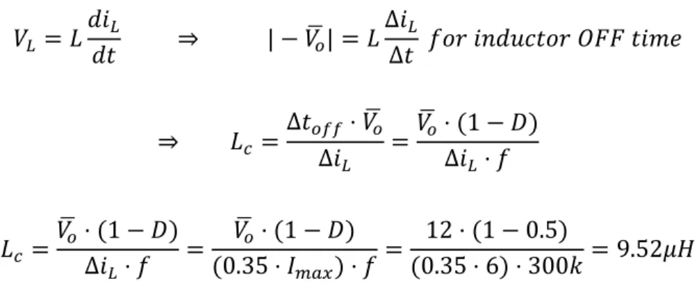
The step-down converter, the LT3845 [24] was chosen. It is a high voltage
synchronous buck converter which operates at a typical value of 300kHz and up to 60V.
The voltage rating is higher than needed, but is useful to account for any spikes from the
renewable energy sources without using any extra protection device. The converters are
to step down from a nominal 24V with a swing of ±6V to 12V. This yields a duty cycle
of approximately 50%. The converter component values were sized according to the
desired values. When sizing an inductor for the converter, the biggest consideration is the
inductor current because of the loss it can impact with the DC resistance (DCR) of the
inductor. Therefore, choosing an inductor with small DC resistance is crucial. Also, as
current through the inductor increases, the inductor eventually begins to saturate and
behaves like a resistor and the value of the inductor decreases. Therefore, it is necessary
to choose a higher value inductor to compensate for the loss of inductance. The critical
inductance was calculated using the equation that is derived below.
𝐷𝑢𝑡𝑦 𝐶𝑦𝑐𝑙𝑒, 𝐷 = 𝑉𝑜 𝑉𝑖𝑛 =
23 𝑉𝐿 = 𝐿
𝑑𝑖𝐿
𝑑𝑡 ⇒ | − 𝑉̅ | = 𝐿𝑜 ∆𝑖𝐿
∆𝑡 𝑓𝑜𝑟 𝑖𝑛𝑑𝑢𝑐𝑡𝑜𝑟 𝑂𝐹𝐹 𝑡𝑖𝑚𝑒
⇒ 𝐿𝑐 =
∆𝑡𝑜𝑓𝑓⋅ 𝑉̅𝑜
∆𝑖𝐿 =
𝑉̅ ⋅ (1 − 𝐷)𝑜 ∆𝑖𝐿⋅ 𝑓
𝐿𝑐 =𝑉̅ ⋅ (1 − 𝐷)𝑜 ∆𝑖𝐿⋅ 𝑓 =
𝑉̅ ⋅ (1 − 𝐷)𝑜 (0.35 ⋅ 𝐼𝑚𝑎𝑥) ⋅ 𝑓 =
12 ⋅ (1 − 0.5)
(0.35 ⋅ 6) ⋅ 300𝑘 = 9.52𝜇𝐻
As shown in the above calculation, the peak to peak current ripple 𝛥𝑖𝐿 is chosen to
be 35% of the maximum output current. This is to follow the common practice of
choosing 𝛥𝑖𝐿 to be in between 30% to 40%. In order to compensate for the loss of
inductance, a higher inductor value, 15𝜇H, was chosen. As seen in Figure 4-5, for the
inductor MPX1D1264L220 inductor [25] whose nominal value is 22𝜇H, its inductance
decreases down to around 17𝜇H at 6A.
24
Next, the following equations that are followed by their derivations were used to
size the critical output capacitance.
𝑞 = 𝐶𝑜∙ ∆𝑉𝑜 ⇒ +𝑞 𝑎𝑟𝑒𝑎 𝑜𝑓 𝑡ℎ𝑒 𝑖𝑐,𝑜𝑢𝑝𝑢𝑡(𝑡) 𝑤𝑎𝑣𝑒𝑓𝑜𝑟𝑚 = 𝐶𝑜∙ ∆𝑉𝑜
⇒ 1 2∙
∆𝑖𝐿 2 ∙
𝑇
2= 𝐶𝑜∙ ∆𝑉𝑜 ⇒ ∆𝑖𝐿
8 ∙ 𝑓 = 𝐶𝑜∙ ∆𝑉𝑜
Thus,
𝐶𝑜 = ∆𝑖𝐿 ∆𝑉𝑜∙ 8𝑓 = [
𝑉̅ ∙ (1 − 𝐷) ∙ 𝑇𝑜
𝐿 ]
1 ∆𝑉𝑜∙ 8𝑓 =
𝑉̅ ∙ (1 − 𝐷)𝑜
∆𝑉𝑜∙ 8𝐿 ∙ 𝑓2 =
(1 − 𝐷) ∆𝑉𝑜
𝑉̅ ∙ 8𝐿 ∙ 𝑓𝑜 2
𝐶
𝑜=
∆𝑉𝑜(1−𝐷)𝑉𝑜
̅̅̅̅ ∙ 8𝐿 ∙ 𝑓2
, where ∆𝑉𝑜
𝑉̅̅̅𝑜 is chosen as 2%, or 0.02
𝐶𝑜= 1 − 0.5 0.02 ⋅ 8 ⋅ 𝐿 ⋅ 𝑓2 =
0.5
1.6 ⋅ 9.52𝜇 ⋅ 300𝑘2 = 3.65𝜇𝐹
Then, for the critical input capacitance equation is derived below.
𝑞 = 𝐶𝑖𝑛∙ ∆𝑉𝑖𝑛 ⇒ −𝑞 𝑎𝑟𝑒𝑎 𝑜𝑓 𝑡ℎ𝑒 𝑖𝑐,𝑖𝑛𝑝𝑢𝑡(𝑡) 𝑤𝑎𝑣𝑒𝑓𝑜𝑟𝑚 = 𝐶𝑖𝑛∙ ∆𝑉𝑖𝑛
𝐶𝑖𝑛 =𝐼̅𝑠𝑤𝑚𝑎𝑥∙ (1 − 𝐷)𝑇
∆𝑉𝑖𝑛 =
𝐷 ∙ 𝐼̅𝑜𝑚𝑎𝑥∙ (1 − 𝐷)𝑇
∆𝑉𝑖𝑛 =
𝐷(1 − 𝐷)𝑉̅𝑜
∆𝑉𝑖𝑛∙ 𝑓 ∙ 𝑅𝑚𝑖𝑛
Thus,
𝐶
𝑖𝑛=
𝐷(1−𝐷)𝑉̅𝑜 ∆𝑉𝑖𝑛∙𝑓∙𝑅𝑚𝑖𝑛,where
𝑅
𝑚𝑖𝑛=
𝑉𝑜𝐼𝑚𝑎𝑥
=
12𝑉
6𝐴
= 2𝛺
and 𝛥𝑉
𝑖𝑛= 2% 𝑜𝑓 24𝑉 = 24𝑉 ⋅ 0.02
𝐶𝑖𝑛 = 0.5 ⋅ (1 − 0.5) ⋅ 12
25
In practice, 2% peak to peak voltages in relation to its average voltage is typically
used as the maximum voltage ripple requirement. A larger output capacitance value was
chosen to smooth the output voltage even more at the expense of a slower transient
response and cost. However, the transient time in this project is not considered as
important as the accuracy of the output voltage. Therefore, a large value of 100𝜇𝐹 was
chosen to minimize the output ripples. By the same token, a larger 80𝜇𝐹 for Cin was also
chosen. Additionally, when sizing the output capacitor, another important consideration
is the capacitor’s equivalent series resistance (ESR). As stated previously, the output
capacitors help minimize the ripples of the output voltage and so one technique to reduce
ESR is by placing output capacitors in parallel. Furthermore, as voltage is applied across
a capacitor, the value of the capacitance decreases. Following these considerations, four
capacitors were used: two 68𝜇𝐹, one 22𝜇𝐹, and one 1𝜇𝐹 capacitor. After the decrease of
the capacitance value of the four capacitors, the total capacitance amounts to around
100𝜇𝐹. Similarly, the multiple input capacitors were used to help decrease ESR and
ripple, resulting in the use of one 47𝜇𝐹and two 2.2𝜇𝐹.
The Rsense is another important component of the buck converter since it is used to
monitor the current through the inductor. The value was calculated from the following
equation in the LT3845 datasheet, where 𝐼𝑜𝑢𝑡,𝑚𝑎𝑥 is around 6A.
𝑅𝑠𝑒𝑛𝑠𝑒 = 70𝑚𝑉 𝐼𝑜𝑢𝑡,𝑚𝑎𝑥 =
70𝑚𝑉
6𝐴 = 11.667𝑚𝛺
Therefore, a sense resistor value of 10𝑚𝛺 was chosen since it is the closest
26
As for the MOSFET in the buck converter, there are many factors to consider
when choosing MOSFET. As stated previously, the main factors to consider when sizing
a MOSFET include the maximum voltage, average current, power, and junction
temperature. The same MOSFET as the ones used for the first stage of the design,
AO4484, can also be used for the buck converter since it meets all of the design
specifications. In the simulations, the results of the MOSFET at boundary conditions is as
follows: the maximum voltage spike is 24.6V, the average current is 6A, and the average
power is 195mW bringing the MOSFET to a maximum of 40°C.
Lastly, the feedback resistors were changed in hopes of making the resolution of
the injected voltage better. Even though decreasing the feedback resistors did not change
the resolution of the injected voltage, the new resistor values were kept, as they are
standard resistor values, readily available, and this resistor divider combination makes a
desired higher output voltage of the buck converter than the intended 12V. The output
voltage was intended to be higher than 12V to account for the diode drops after the buck
converters. The resistor R1 of Figure 4-6 was first chosen to be 9.53k𝛺 as it is a nominal
1% standard resistor. Then, R2 of Figure 4-6 was then calculated by the following
equation found in the LT3845 datasheet.
𝑅2 = 𝑅1 ⋅ ( 𝑉𝑜𝑢𝑡
1.231𝑉− 1), where Vout = 12.7V and R1 = 9.53k𝛺
𝑅2 = 9.53𝑘 ⋅ ( 12.7
27
Figure 4-6: Resistor divider on external pin of VFB.
A nominal 5% resistor of 91k𝛺 was then chosen, as it is a readily available
resistor. The value of R1 and R2 from the datasheet corresponds to R6, R13 and R5, R12 of
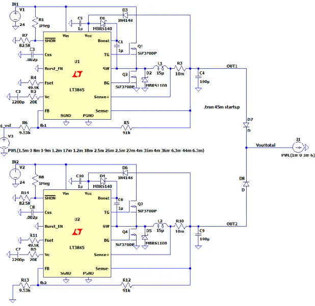
the simulations in Figure 4-7, respectively.
Next, the design is simulated in LTSpice. However, since the first stage deals with
making the decision of using one or two converters, therefore only the second stage
consisting the actual converters is simulated. The goal of the simulations in LTSpice of
the MISO converter is to be able to unevenly split current between the two converters,
which will eventually combine to the value of the load current while maintaining an
output voltage of 12V. The load current will vary from 5A to 7A, with the current rating
of the individual converters to be rated at 6.25A. Following the first stage of determining
which converter should be connected to the output, the converters are first set in parallel,
28
Figure 4-7: Circuit with two paralleled buck converters used to unevenly split current.
The loading current will differ depending on what application is needed and, in
this project, will be varied from 5A to 7A. The injected voltage is applied to the feedback
pin of only the first converter, while the second converter’s feedback pin is connected to
ground. Injecting voltage to only one converter allows for more convenient testing, as
there are less variables to monitor while testing. The feedback pin of a step-down
29
datasheet, the converter desires an external voltage of 1.231V at the feedback pin for an
output of 12V. This external voltage is internally connected into an error amplifier. If the
voltage is not at 1.231V, the buck converter will act accordingly and adjust the output
voltage until it returns back to 12V output. In this simulation, a small positive voltage is
applied to the feedback pin, in which the output voltage decreases slightly. Doing so will
trick the converter into believing that the output voltage had reached the desired 12V.
Therefore, as the injected voltage at the feedback pin increases, the output voltage will
decrease slightly, thereby the output current of the converter must act appropriately by
decreasing its value. Because the second converter does not have a voltage injected at the
feedback pin, it will behave like a regular buck converter; however, it will output a
current that ensures that the sum of the two currents from the converters add up to the
demanded output load current. In this simulation, output voltages of 12.7V from each
individual converters are desired since two diodes are placed following the converters to
prevent any backflow of current into the buck. After the diode drop of around 0.7V, the
30
Figure 4-8: Simulation of current splitting with 6A load current.
Figure 4-8 illustrates the simulation of the paralleled buck converters with a 6A
load. The total output voltage waveform illustrates that it is always around 12V. Near the
beginning of the simulation, at around 1.5ms, the current starts to split into a 50/50 ratio.
At this time, there is a slight drop, 0.7V, on the total voltage output due to the voltage
drop across the diodes. We can also observe from Figure 4-8 that the output voltage
actually decreases very little as the injected voltage increases. As the output voltage starts
to steady out at its own particular voltage per injected voltage value, the feedback voltage
31
voltage is at the right level and to stop increasing or decreasing the output voltage. In the
simulations, as the injected voltage starts to increase, the output voltage decreases very
slightly, in which the output current also decreases.
The model used in this simulation is close to an ideal model. This means there are
no stray and parasitic components incorporated in the model. This results in the same
efficiency curves of the two converters. Figure 4-9 illustrates the efficiency curves of the
identical converters with load currents 6A, 7A, and 8A.
Figure 4-9: Efficiency vs. percentage load current percentage with identical converters.
In practice, the converters will not be identical to each other. For example, the DC
resistance (DCR) of the inductor in one converter or the actual switching frequency of
one converter may be slightly different from the other. With these minor differences, the
efficiency curves of the individual converters will be different. The uneven splitting of 91
92 93 94 95 96 97 98
0 10 20 30 40 50 60 70 80 90
E
ff
icien
cy
(
%)
Load Current of Converter 1 (%)
Efficiency vs. Perecentage Load Current of Converter 1
6A Load Current
7A Load Current
32
current between the two individual converters will then be recorded by the Arduino.
Then, the Arduino will be able to determine which current ratio, and the injected voltage,
to produce in order to achieve the greatest efficiency.
With DCR of 0.0833Ω on one converter, no DCR on the other converter, and a
total output load current of 6A, the efficiency curves are shown in Figure 4-10. The DCR
of 0.0833Ω was chosen to force 3W loss at the output. Because 𝑃 = 𝐼2⋅ 𝑅, and P = 3W
and I = 6A, R = 0.0833Ω. This illustrates that with minor parasitic losses, the efficiency
may decrease dramatically. As depicted in Figure 4-10, at all load current percentages the
converter with no DCR will always be more efficient than its counterpart.
Figure 4-10: Efficiency vs. percentage of 6A load current; one converter with DCR =
0.08Ω and one converter with no DCR.
Another case that was tested is if both converters have DCR, one much larger
than the other. A DCR value of 0.0833Ω was chosen to force a 3W loss at the output, and 90
91 92 93 94 95 96 97 98
0 20 40 60 80 100
E
ff
icien
cy
(
%)
Load Current of Converter 1 (%)
Efficiency vs. Percentage Load Current with 6A Load Current with one converter DCR = 0.0833Ω and one converter with no DCR
33
a DCR value of 0.5Ω was chosen to force a 18W loss at the output. These two extreme
DCR values are used in order to demonstrate that the differences in the two converters
will illustrate different efficiency graphs. Figure 4-11 illustrates that DCR decreases the
efficiency of the converter. With these efficiency graphs, it is clearly more efficient to run
at 20% load current when DCR is 0.5Ω and 80% load current when DCR is 0.08Ω rather
than the combination of 80% load current when DCR is 0.5Ω and 20% load current when
DCR is 0.08Ω.
Figure 4-11: Efficiency vs percentage of 6A load current; one converter with DCR =
0.08Ω and one converter with DCR = 0.5Ω.
Another practical scenario that may produce differences in efficiency curves is if
the switching frequencies of the two converters are not matched. Currently, the typical
switching frequency of the LT3845 converters are 300kHz. The LT3845 datasheet 80
82 84 86 88 90 92 94 96 98
0 20 40 60 80 100
E
ff
icien
cy
(
%)
Load Current [%]
Efficiency vs. Percentage Load Current with 6A Load Current, both Converters with DCR
34
illustrates how to change the switching frequency by calculating for the external resistor
at the Fset pin:
𝑅𝑠𝑒𝑡 = 8.4 ⋅ 104⋅ 𝑓
𝑠𝑤(−1.31),
where 𝑅𝑠𝑒𝑡 is in kΩ and 𝑓𝑠𝑤 is in kHz
For a switching frequency of 300kHz, the Rset value of both converters should be
47.78kΩ. Therefore, the closest standard resistor value is 47kΩ. However, it is very likely
that the resistor values between the two converters will differ by a tiny amount. For a
resistor tolerance of ±5%, the worst-case scenario will be when one converter’s Rset value
is -5%, 44.65kΩ, and when the other converter’s Rset value is +5%, 49.35kΩ. Therefore,
with these two different Rset values, the corresponding frequencies are 315.93kHz and
292.69kHz, respectively, which have been calculated from the aforementioned equation.
No DCR is added to this simulation to have less variables while testing. Figure 4-12
illustrates the two different efficiency curves when the switching frequencies differ
35
Figure 4-12: Efficiency vs. percentage of 6A load current; one converter with R-5% and
one converter with R+5%.
As illustrated in Figure 4-12, the switching frequency does not affect the
efficiency too much, and the slight differences in resistances, thus frequencies, are
negligible.
As illustrated from the simulations, different parasitics may introduce a change in
efficiency. Initially, when the converters are perfectly the same in simulation, there is
hardly any difference with varying loads. However, once parasitics are introduced, the
efficiency graphs change to match the amount of losses from the buck converter; the
more parasitics the efficiency will most likely decrease. The differences in efficiencies
between the two converters illustrate that the specific choosing of different ratios can
result in the maximum efficiency of the circuit. Ultimately, simulation proved that the 90
91 92 93 94 95 96 97 98
0 20 40 60 80 100
E
ff
icien
cy
(
%)
Load Current (%)
Efficiency vs. Percentage Load Current at Output Load 6A, Converter 1 with Rset - 5% and Converter 2 with Rset + 5%
Rset - 5%
36
splitting of currents was successful when applying a small voltage in place of the ground
37 5. HARDWARE DESIGN AND RESULTS
In this chapter, the hardware design, construction, and results are discussed.
The stage 1, shown in Figure 5-1, is used as a passthrough stage. The Arduino
will be utilized to apply 0V or 5V to the input of the gate driver to turn on or off switches
S1 and S2. More specifically the 0V from the Arduino will open the switch while the 5V
signal will close the switch.
Figure 5-1: Block diagram of stage 1, passthrough stage.
Stage 1 is solely used to allow the circuit to use either converter 1 or both
converters at once. Because there is a diode between the power paths, current will only be
able to flow from the bottom power path to the top power path, which means that only
converter 1, and not just converter 2, can be used by itself. All but one ratio case will
have S1 open and S2 closed. Only one case will close S1 and open S2, which is the 100%
/ 0% ratio case where only converter 1 will be used.
For testing stage 1, there were two loads used on the two outputs of the board.
38
Figure 5-2: Test setup of stage 1.
There were two parts done during this test. The DC electronic loads were set to
1A per output. The first test was to turn off (open) switch S1 and to turn on (close) switch
S2. This configuration occurs when the current will split unevenly between the two
converters for all the different ratios except for 100% / 0%. The Arduino was
programmed to turn off switch S1 by providing 0V to the input pin of the first gate driver,
and to turn on switch S2 by providing 5V to the input pin of the second gate driver.
Figure 5-4 illustrates that the top DC electronic load, which belongs to the path of switch
S1, pulls in 0A, and that the bottom DC electronic load, which belongs to the path of
switch S2, has 1A running through it. Additionally, the power supply is supplying 1A,
39
Figure 5-3: Part of Arduino code illustrating switch S1 off and switch S2 on.
Figure 5-4: Test results for switch S1 off and switch S2 on.
The next test was to test the opposite, where switch S1 is closed (turned on), and
switch S2 is open (turned off). This configuration is to test the 100% / 0% load current
40
switch S1 by providing 5V to the input pin of the first gate driver, and to turn off switch
S2 by providing 0V to the input pin of the second gate driver. Figure 5-6 illustrates that
the top DC electronic load, which belongs to the path of switch S1, pulls in 1A, and that
the bottom DC electronic load, which belongs to the path of switch S2, has no current
running through it. Additionally, the power supply is supplying 1A, suggesting that only
one path with 1A is running through it. Figure 5-7 illustrates the physical protoboard for
stage 1, the passthrough stage.
41
Figure 5-6: Test results for switch S1 on and switch S2 off.
42
The block diagram of Stage 2, which combines the outputs of the converters into
one single 12V bus, has been modified from Chapter 4 to illustrate the injected voltages
to both converters as seen in Figure 5-8.
Figure 5-8: Block diagram of stage 2, uneven current sharing.
In the previous chapter, the applied voltage at the FB node was supposed to be
done only to the top converter. However, as the hardware testing progressed, it was
determined that it would be more convenient to apply voltages at both FB nodes to help
create the different ratios.
As stated in the previous chapter, this stage’s goal is to unevenly split the load
current between the two converters. The uneven splitting of the load current is done by
applying a small voltage at the feedback pins of the converters. On both of the LT3845
demo boards, the 0402-sized R8 and R9, as seen highlighted in Figure 5-9, and its demo
board in Figure 5-10, were replaced with 9.53kΩ and 91kΩ resistors. Both figures were
43
grounded part of R8 was then lifted from the ground trace and connected by a wire to the
DAC’s current to voltage amplifier OPA2277, which are both on the protoboard.
Figure 5-9: Schematic of LT3845 demo board, R8 and R9 highlighted.
44
Prior to modifying the demo board, Linear Technology stated that it could take a
Vin that would range from 20V to 55V and would be able to output 12V at 6.25A. During
testing, the demo board could only operate up to 5A, most likely due to the different FB
resistor values that allows for higher output voltage. The reason for a desired higher
output voltage is to account for the diode drop following the converters. Because the
RIGOL DP832 DC Power Supply has a maximum power output of 90W, the higher the
load current means that the power supply will need to deliver more current. Once the
power supply outputs 90W, its voltage will drop to meet the power supply’s output power
requirement. Therefore, all of the data taken had a current limit of 5A per converter.
The Vout and GND from both demo boards then connect to the second protoboard.
The voltage sensors, which are resistor dividers of 75kΩ and 11kΩ, then take in the
resistor divider values and are calculated back with the Arduino from which the user can
observe the voltages on their PC. Diodes are then placed after the inputs into the
protoboard. Then, 10mΩ resistors are used with the INA169 current sensors, in which the
voltage outputs of the INA169 are connected to the analog in pins of the Arduino and are
converted back into current that the user can observe. Both the voltage sensors and
current sensors are observable to the user using serial communication with Arduino.
After the current sensors, the two output voltages are then combined into a single output,
which has an output of around 12V. The block diagram of the test configuration setup for
45
Figure 5-11: Test configuration setup of stage 2.
After testing stage 2, the addition of stage 1 was implemented in conjunction with
stage 2. The entire setup, with stage 1 and stage 2 connected, is shown in Figure 5-12.
Figure 5-13 illustrates stage 2, the demo boards in parallel with the protoboard and
Arduino. Figure 5-14 shows a closer look of the stage 2 protoboard.
46
Figure 5-13: Stage 2, demo boards in parallel with protoboard and Arduino.
47
The DAC8801 and OPA2277 supplied the small negative voltage to the FB
nodes. DAC8801 is a 14-bit DAC that outputs a current and works with the OPA2277
current to voltage amplifier. Both the DAC8801 and OPA2277 are high precision, with
little noise or error. This is vital to the purpose of the DAC in this project, as the injected
voltage is extremely sensitive in the millivolts range. The OPA2277 outputs a negative
voltage, in which the injected voltage and load current percent, which was mentioned
previously in Chapter 4, will actually be switched between the two converters. Because
of the noise from the long cables to connect from board to board, the DAC code can be
slightly inconsistent with its corresponding DAC voltage.
Next, the two stages were then put together and tested. Originally, in Chapter 3, it
was stated that only 3A would be used as the output load current. This was changed in
Chapter 4, where the output load current was changed from 5A to 7A.
Tables 5-1 and 5-2 list the current split between the two converters, in addition to the
48
Table 5-1: Uneven Current Splitting and Efficiencies of Converter 1 with 5A Load
Current.
ILoad Percentage (%) Vin [V] Iin [A] Vout [V] Iout [A] Efficiency (%)
0 24.01 0.04 12.84 0 0
10 23.94 0.31 12.67 0.50 85.36
20 23.93 0.57 12.60 1.00 92.37
30 23.92 0.83 12.40 1.50 93.62
40 23.90 1.09 12.25 2.00 94.23
50 23.89 1.34 12.12 2.50 94.65
60 23.89 1.64 12.36 3.00 94.64
70 23.93 1.95 12.58 3.50 94.35
80 23.87 2.28 12.88 4.002 94.71
90 23.88 2.62 13.15 4.50 94.58
49
Table 5-2: Uneven Current Splitting and Efficiencies of Converter 2 with 5A Load
Current.
ILoad Percentage (%) Vin [V] Iin [A] Vout [V] Iout [A] Efficiency (%)
100 23.86 2.97 12.82 4.99 90.45
90 23.88 2.57 12.65 4.50 92.75
80 23.87 2.24 12.49 4.00 93.43
70 23.93 1.92 12.30 3.50 93.72
60 23.89 1.61 12.10 2.99 94.25
50 23.89 1.32 11.93 2.50 94.57
40 23.90 1.07 12.18 2.00 95.25
30 23.92 0.81 12.43 1.50 96.23
20 23.93 0.56 12.67 0.99 94.35
10 23.94 0.30 12.93 0.50 90.01
0 24.01 0.06 13.41 0 0
These two tables illustrate the uneven current sharing between the two converters. For
example, the column of ILoad percentage of converter 1 is 40% illustrating that Iout is
2.004A while the column of ILoad percentage of converter 2 is 60% illustrating that Iout is
2.996A. Note that the total load current for this example is 5A. While testing, there were
some inconsistencies with the output voltage of the converters. The DAC provides a
50
That varying node is essentially a floating node since the feedback of the converter is not
actually referencing ground which is why Vout varies slightly. Figure 5-15 illustrates the
efficiency versus load current percentage curve for the data in the above tables.
Figure 5-15: Efficiency vs. Percentage load current with 5A load current.
The two curves are close to each other, which means that the two converters have slight
dissimilarities. However, even though the efficiencies of the two converters look similar,
the differences per current ratio do contribute to differences in total efficiencies.
Because there is no current sensor and voltage sensor at the output of the entire
circuit, the efficiency of the system is determined by the following equations. 0
10 20 30 40 50 60 70 80 90 100
0 20 40 60 80 100
E
ff
icien
cy
(
%)
Load Current Percent (%)
Efficiency vs. Percentage Load Current with Load Current 5A
Converter 1
51
𝐸𝑓𝑓𝑖𝑐𝑖𝑒𝑛𝑐𝑦
𝑇𝑜𝑡𝑎𝑙=
𝑃
𝑜𝑢𝑡1+ 𝑃
𝑜𝑢𝑡2𝑃
𝑖𝑛1+ 𝑃
𝑖𝑛2𝐸𝑓𝑓𝑖𝑐𝑖𝑒𝑛𝑐𝑦
𝑇𝑜𝑡𝑎𝑙=
(𝑉
𝑜𝑢𝑡1⋅ 𝐼
𝑜𝑢𝑡1) + (𝑉
𝑜𝑢𝑡2⋅ 𝐼
𝑜𝑢𝑡2)
(𝑉
𝑖𝑛1⋅ 𝐼
𝑖𝑛1) + (𝑉
𝑖𝑛2⋅ 𝐼
𝑖𝑛2)
This equation disregards the voltage diode drop following the converters, as there is no
voltage or current sensors at the combined single output. The Arduino will then calculate
the total efficiency of each current split ratio. Table 5-3 lists the results of this calculation
with load current of 5A which are then graphed as shown in Figure 5-16.
Table 5-3: Total Efficiencies with 5A Load Current.
Load Current Ratio of Converter 1 to Converter 2 (% / %)
Total Efficiency (%)
0/100 89.25
10/90 91.96
20/80 93.22
30/70 93.69
40/60 94.24
50/50 94.61
60/40 94.88
70/30 94.91
80/20 94.64
90/10 94.11
52
Figure 5-16: Overall efficiency vs. load current percentage of converter 1 with 5A load
current.
As evident from Figure 5-16, the current ratio of 70/30 at 5A load current will be most
efficient. The Arduino will then alter the DAC value to match the 70/30 current split ratio
so that the total efficiency of the system will be at its highest.
Table 5-4 and 5-5 illustrate the uneven current sharing in addition to the
efficiencies when the load current is at 6A for converter 1 and converter 2.
89.25 91.96 93.22 93.69 94.24 94.61 94.88 94.91 94.64 94.11 93.05 88 89 90 91 92 93 94 95 96
0 10 20 30 40 50 60 70 80 90 100
Ov er all E ff icien cy ( %)
Percentage Load Current of Converter 1 (%)
53
Table 5-4: Uneven Current Splitting and Efficiencies of Converter 1 with 6A Load
Current.
ILoad Percentage (%) Vin [V] Iin [A] Vout [V] Iout [A] Efficiency (%)
20 23.92 0.68 12.48 1.19 91.91
30 23.90 0.99 12.27 1.80 93.34
40 23.90 1.29 12.18 2.39 94.73
50 23.91 1.60 11.92 3.00 93.47
60 23.90 1.95 12.24 3.59 94.28
70 23.89 2.34 12.64 4.20 95.05
80 23.90 2.74 12.93 4.80 94.77
Table 5-5: Uneven Current Splitting and Efficiencies of Converter 2 with 6A Load
Current.
ILoad Percentage (%) Vin [V] Iin [A] Vout [V] Iout [A] Efficiency (%)
80 23.90 2.68 12.57 4.80 94.23
70 23.89 2.28 12.27 4.20 94.61
60 23.9 1.92 11.98 3.60 94.03
50 23.91 1.54 11.73 3.00 95.56
40 23.9 1.27 11.94 2.41 94.80
30 23.9 0.96 12.15 1.79 95.10
54
Data from Tables 5-4 and 5-5 were then plotted as shown in Figure 5-17. Note that with
these sets of data, the load current percentages range from 20% to 80%. This is due to the
fact that at any currents higher than 80% of 6A, the converters will run over their current
limit of 5A. By the same reasoning, the 7A load test case has data points ranging from
30% to 70%.
Figure 5-17: Efficiency vs. Percentage load current with 6A load current.
Using the same previous equation, the Arduino code produces the ratio with the highest
total efficiency. Table 5-6 and Figure 5-18 illustrate the total efficiencies for each of the
different ratios. 91.5 92.0 92.5 93.0 93.5 94.0 94.5 95.0 95.5 96.0
0 20 40 60 80 100
E
ff
icien
cy
(
%)
Load Current Percent (%)
Efficiency vs. Load Current Percentages with Load Current 6A
Converter 1
55
Table 5-6: Total Efficiencies with 6A Load Current.
Load Current Ratio of Converter 1 to Converter 2 (% / %)
Total Efficiency (%)
20/80 93.77
30/70 94.23
40/60 94.32
50/50 94.50
60/40 94.49
70/30 95.07
80/20 94.61
Figure 5-18: Overall efficiency vs. load current percentage of converter 1 with 6A load
current. 93.77 94.23 94.32 94.50 94.49 95.07 94.61 93.6 93.8 94.0 94.2 94.4 94.6 94.8 95.0 95.2
0 20 40 60 80 100
Ov er all E ff icien cy ( %)
Percentage Load Current of Converter 1 (%) Overall Efficiency (%) vs. Load Current Percentage of
![Figure 2-1: Full bridge converter with phase shift pulse width modulation with two inputs [10]](https://thumb-us.123doks.com/thumbv2/123dok_us/8221909.2179802/18.918.344.628.107.419/figure-bridge-converter-phase-shift-pulse-modulation-inputs.webp)
![Figure 2-2: Multiple input DC to DC soft-switching edge-resonant converter with two inputs [12-13]](https://thumb-us.123doks.com/thumbv2/123dok_us/8221909.2179802/19.918.313.662.247.565/figure-multiple-input-soft-switching-resonant-converter-inputs.webp)