BGS2-E/BGS2-W
Version:
01.301
DocId:
BGS2_HID_v01.301
GENERAL NOTE
THE USE OF THE PRODUCT INCLUDING THE SOFTWARE AND DOCUMENTATION (THE "PROD-UCT") IS SUBJECT TO THE RELEASE NOTE PROVIDED TOGETHER WITH PRODUCT. IN ANY EVENT THE PROVISIONS OF THE RELEASE NOTE SHALL PREVAIL. THIS DOCUMENT CONTAINS INFORMATION ON CINTERION PRODUCTS. THE SPECIFICATIONS IN THIS DOCUMENT ARE SUB-JECT TO CHANGE AT CINTERION'S DISCRETION. CINTERION WIRELESS MODULES GMBH GRANTS A NON-EXCLUSIVE RIGHT TO USE THE PRODUCT. THE RECIPIENT SHALL NOT TRANS-FER, COPY, MODIFY, TRANSLATE, REVERSE ENGINEER, CREATE DERIVATIVE WORKS; DISAS-SEMBLE OR DECOMPILE THE PRODUCT OR OTHERWISE USE THE PRODUCT EXCEPT AS SPECIFICALLY AUTHORIZED. THE PRODUCT AND THIS DOCUMENT ARE PROVIDED ON AN "AS IS" BASIS ONLY AND MAY CONTAIN DEFICIENCIES OR INADEQUACIES. TO THE MAXIMUM EXTENT PERMITTED BY APPLICABLE LAW, CINTERION WIRELESS MODULES GMBH DISCLAIMS ALL WARRANTIES AND LIABILITIES. THE RECIPIENT UNDERTAKES FOR AN UNLIMITED PERIOD OF TIME TO OBSERVE SECRECY REGARDING ANY INFORMATION AND DATA PROVIDED TO HIM IN THE CONTEXT OF THE DELIVERY OF THE PRODUCT. THIS GENERAL NOTE SHALL BE GOV-ERNED AND CONSTRUED ACCORDING TO GERMAN LAW.
Copyright
Transmittal, reproduction, dissemination and/or editing of this document as well as utilization of its con-tents and communication thereof to others without express authorization are prohibited. Offenders will be held liable for payment of damages. All rights created by patent grant or registration of a utility model or design patent are reserved.
Copyright © 2011, Cinterion Wireless Modules GmbH
Trademark Notice
Microsoft and Windows are either registered trademarks or trademarks of Microsoft Corporation in the United States and/or other countries. All other registered trademarks or trademarks mentioned in this doc-ument are property of their respective owners.
Document Name:
BGS2-E/BGS2-W Hardware Interface Description
Version:
01.301
Date:
2011-04-07
DocId:
BGS2_HID_v01.301
Contents
0 Document History ... 9
1 Introduction ... 10
1.1 Related Documents ... 10
1.2 Terms and Abbreviations ... 10
1.3 Regulatory and Type Approval Information ... 14
1.3.1 Directives and Standards... 14
1.3.2 SAR requirements specific to portable mobiles ... 17
1.3.3 Safety Precautions... 18
2 Product Concept ... 19
2.1 Key Features at a Glance ... 19
2.2 BGS2-E/BGS2-W System Overview... 21
2.3 Circuit Concept ... 22
3 Application Interface... 23
3.1 Operating Modes ... 24
3.2 Power Supply... 25
3.2.1 Minimizing Power Losses ... 25
3.2.2 Measuring the Supply Voltage (VBATT+) ... 26
3.2.3 Monitoring Power Supply by AT Command ... 26
3.3 Power Up/Power Down Scenarios... 27
3.3.1 Turn on BGS2-E/BGS2-W ... 27
3.3.1.1 Switch on BGS2-E/BGS2-W Using ON Signal... 27
3.3.1.2 Suppressing Unintentional Pulses on ON Signal Line ... 29
3.3.1.3 Turn on BGS2-E/BGS2-W Using the RTC (Alarm Mode) ... 30
3.3.2 Restart BGS2-E/BGS2-W ... 30
3.3.2.1 Restart BGS2-E/BGS2-W via AT+CFUN Command... 30
3.3.2.2 Restart BGS2-E/BGS2-W Using EMERG_RST... 31
3.3.3 Signal States after Startup ... 32
3.3.4 Turn off BGS2-E/BGS2-W ... 34
3.3.4.1 Switch off BGS2-E/BGS2-W Using AT Command ... 34
3.3.5 Automatic Shutdown ... 36
3.3.5.1 Thermal Shutdown ... 36
3.3.5.2 Undervoltage Shutdown ... 37
3.3.5.3 Overvoltage Shutdown ... 37
3.4 Automatic GPRS Multislot Class Change ... 38
3.5 Power Saving... 39
3.5.1 No Power Saving (AT+CFUN=1) ... 39
3.5.2 NON-CYCLIC SLEEP Mode (AT+CFUN=0)... 39
3.5.3 CYCLIC SLEEP Mode AT+CFUN=7 ... 40
3.5.4 CYCLIC SLEEP Mode AT+CFUN=9 ... 40
3.5.6 Wake up BGS2-E/BGS2-W from SLEEP Mode... 42
3.5.6.1 Wake-up via RTS0 and RTS1 (if AT+CFUN=0 or AT+CFUN=9)... 43
3.6 Summary of State Transitions (except SLEEP Mode) ... 43
3.7 RTC Backup... 44
3.8 SIM/USIM Interface... 45
3.9 Serial Interface ASC0 ... 47
3.10 Serial Interface ASC1 ... 50
3.11 Analog Audio Interface... 52
3.11.1 Microphone Inputs and Supply ... 52
3.11.2 Loudspeaker Output ... 54
3.12 GPIO Interface ... 55
3.13 I2C Interface ... 57
3.14 PWM Interfaces ... 59
3.15 Status LED... 59
3.16 Behavior of the RING0 Line (ASC0 Interface only)... 60
3.17 Power Indication Circuit ... 61
4 Antenna Interface... 63
4.1 Antenna Installation ... 64
4.2 RF Line Routing Design... 65
4.2.1 Line Arrangement Examples... 65
4.2.1.1 Embedded Stripline ... 65
4.2.1.2 Micro-Stripline ... 66
4.2.2 Routing Example... 70
4.2.2.1 Interface to RF Connector... 70
5 Electrical, Reliability and Radio Characteristics... 71
5.1 Absolute Maximum Ratings ... 71
5.2 Operating Temperatures... 72
5.3 Reliability Characteristics... 73
5.4 Pad Assignment and Signal Description... 74
5.5 Power Supply Ratings... 82
5.6 Electrical Characteristics of the Voiceband Part ... 83
5.6.1 Setting Audio Parameters by AT Commands ... 83
5.6.2 Audio Programming Model ... 84
5.6.3 Characteristics of Audio Modes ... 85
5.6.4 Voiceband Receive Path... 86
5.6.5 Voiceband Transmit Path... 87
5.7 Antenna Interface Specification ... 88
5.8 Electrostatic Discharge ... 89
6 Mechanics, Mounting and Packaging ... 90
6.1 Mechanical Dimensions of BGS2-E/BGS2-W... 90
6.2 Mounting BGS2-E/BGS2-W onto the Application Platform... 92
6.2.1 SMT PCB Assembly ... 92
6.2.1.1 Land Pattern and Stencil ... 92
6.2.2 Moisture Sensitivity Level ... 94
6.2.3 Soldering Conditions and Temperature ... 95
6.2.3.1 Reflow Profile ... 95
6.2.3.2 Maximum Temperature and Duration... 96
6.2.4 Durability and Mechanical Handling... 97
6.2.4.1 Storage Conditions... 97
6.2.4.2 Processing Life... 98
6.2.4.3 Baking ... 98
6.2.4.4 Electrostatic Discharge... 98
6.3 Packaging ... 99
6.3.1 Tape and Reel ... 99
6.3.1.1 Orientation... 99
6.3.1.2 Barcode Label ... 100
6.3.2 Shipping Materials ... 101
6.3.2.1 Moisture Barrier Bag ... 101
6.3.2.2 Transportation Box ... 103
6.3.3 Trays ... 104
7 Sample Application... 105
7.1 Blocking against RF on Interface Lines ... 107
8 Reference Approval ... 109
8.1 Reference Equipment for Type Approval... 109
8.2 Compliance with FCC and IC Rules and Regulations ... 110
9 Appendix... 111
Tables
Table 1: Directives ... 14
Table 2: Standards of North American type approval ... 14
Table 3: Standards of European type approval... 14
Table 4: Requirements of quality ... 15
Table 5: Standards of the Ministry of Information Industry of the People’s Republic of China ... 15
Table 6: Toxic or hazardous substances or elements with defined concentration limits 16 Table 7: Overview of operating modes ... 24
Table 8: Signal states... 32
Table 9: Temperature dependent behavior... 36
Table 10: Wake-up events in NON-CYCLIC and CYCLIC SLEEP modes ... 42
Table 11: State transitions of BGS2-E/BGS2-W (except SLEEP mode) ... 43
Table 12: Signals of the SIM interface (SMT application interface) ... 45
Table 13: DCE-DTE wiring of ASC0 ... 48
Table 14: DCE-DTE wiring of ASC1 ... 50
Table 15: GPIO assignment... 55
Table 16: Power indication circuit ... 61
Table 17: Return loss in the active band... 63
Table 18: Absolute maximum ratings... 71
Table 19: Board temperature ... 72
Table 20: Ambient temperature according to IEC 60068-2 (w/o forced air circulation).. 72
Table 21: Ambient temperature with forced air circulation (air speed 0.9m/s) ... 72
Table 22: Summary of reliability test conditions... 73
Table 23: Pad assignments... 75
Table 24: Electrical description of application interface ... 76
Table 25: Power supply ratings... 82
Table 26: Audio parameters adjustable by AT command ... 83
Table 27: Voiceband characteristics (typical)... 85
Table 28: Voiceband receive path... 86
Table 29: Voiceband transmit path ... 87
Table 30: Antenna interface specifications ... 88
Table 31: Measured electrostatic values... 89
Table 32: Reflow temperature ratings ... 95
Table 33: Storage conditions ... 97
Table 34: EMI measures on the application interface ... 108
Table 35: List of parts and accessories... 111
Figures
Figure 1: BGS2-E/BGS2-W system overview ... 21
Figure 2: BGS2-E/BGS2-W block diagram ... 22
Figure 3: Power supply limits during transmit burst... 25
Figure 4: Position of reference points BATT+and GND ... 26
Figure 5: ON circuit sample... 27
Figure 6: ON timing ... 28
Figure 7: Sample circuit to suppress spikes or glitches on ON signal line ... 29
Figure 8: Emergency restart timing ... 31
Figure 9: Switch off behavior... 35
Figure 10: Timing of CTS signal (example for a 2.12 s paging cycle)... 41
Figure 11: Beginning of power saving if CFUN=7 ... 41
Figure 12: RTC supply variants... 44
Figure 13: External SIM card holder circuit ... 45
Figure 14: VDIG controlled power supply domain... 47
Figure 15: Serial interface ASC0... 48
Figure 16: ASC0 startup behavior ... 49
Figure 17: Serial interface ASC1... 50
Figure 18: ASC1 startup behavior ... 51
Figure 19: Single ended microphone connection ... 53
Figure 20: Differential Microphone connection... 53
Figure 21: Line Input ... 53
Figure 22: Differential loudspeaker connection ... 54
Figure 23: Line output connection... 54
Figure 24: GPIO startup behavior ... 56
Figure 25: I2C interface connected to VCC of application ... 57
Figure 26: I2C interface connected to V180 or V285... 57
Figure 27: I2C startup behavior ... 58
Figure 28: Status signalling with LED driver... 59
Figure 29: Incoming voice call... 60
Figure 30: Incoming voice call... 60
Figure 31: URC transmission ... 60
Figure 32: Power indication circuit ... 62
Figure 33: Antenna pads (bottom view) ... 64
Figure 34: Embedded Stripline with 65µm prepreg (1080) and 710µm core ... 65
Figure 35: Micro-Stripline on 1.0mm standard FR4 2-layer PCB - example 1 ... 66
Figure 36: Micro-Stripline on 1.0mm Standard FR4 PCB - example 2... 67
Figure 37: Micro-Stripline on 1.5mm Standard FR4 PCB - example 1... 68
Figure 38: Micro-Stripline on 1.5mm Standard FR4 PCB - example 2... 69
Figure 39: Pouting to application‘s RF connector - top view ... 70
Figure 40: Numbering plan for connecting pads (bottom view)... 74
Figure 41: Audio programming model ... 84
Figure 42: BGS2-E/BGS2-W– top and bottom view... 90
Figure 43: Dimensions of BGS2-E/BGS2-W (all dimensions in mm) ... 91
Figure 44: Land pattern (top view) ... 92
Figure 45: Recommended design for 110 micron thick stencil (top view) ... 93
Figure 46: Recommended design for 150 micron thick stencil (top view) ... 93
Figure 47: Reflow Profile ... 95
Figure 51: Moisture barrier bag (MBB) with imprint... 101
Figure 52: Moisture Sensitivity Label ... 102
Figure 53: Humidity Indicator Card - HIC ... 103
Figure 54: Small quantity tray... 104
Figure 55: Tray to ship odd module amounts... 104
Figure 56: Trays with packaging materials... 104
Figure 57: Schematic diagram of BGS2-E/BGS2-W sample application ... 106
Figure 58: EMI circuits... 107
0
Document History
Preceding document:"BGS2-E/BGS2-W Hardware Interface Description" Version 00.100b New document:"BGS2-E/BGS2-W Hardware Interface Description" Version 01.301
Preceding document:"BGS2-E/BGS2-W Hardware Interface Description" Version 00.100a New document:"BGS2-E/BGS2-W Hardware Interface Description" Version 00.100b
Preceding document:"BGS2-E/BGS2-W Hardware Interface Description" Version 00.100 New document:"BGS2-E/BGS2-W Hardware Interface Description" Version 00.100a
New document:"BGS2-E/BGS2-W Hardware Interface Description" Version 00.100
Chapter What is new
5.4 Marked pad 64 as AGND pad in Figure 40. 5.4, 6.1 Updated layout for module‘s center pads. 6.2.1.1 Updated section Land Pattern and Stencil. 6.3.3 New section on Trays.
7 Revised Figure 57 to show only two BATT+ pads.
Chapter What is new
2.1 Added module weight. 3.2.2 Added Figure 4.
6.2.1.1 Updated section Land Pattern and Stencil. 6.2.3.1 Updated section Reflow Profile.
6.3.1 Added tape and reel dimensions. 6.3.1.1 Added Figure 48.
Chapter What is new
3.16 Revised RING0 behavior. 6.1 Updated Figure 43.
Chapter What is new
1
Introduction
This document1 describes the hardware of the Cinterion BGS2-E/BGS2-W module that con-nects to the cellular device application and the air interface. It helps you quickly retrieve inter-face specifications, electrical and mechanical details and information on the requirements to be considered for integrating further components.
1.1
Related Documents
[1] BGS2-E/BGS2-W AT Command Set [2] BGS2-E/BGS2-W Release Note
[3] Application Note 48: SMT Module Integration for BGS2-E/BGS2-W
1.2
Terms and Abbreviations
1. The document is effective only if listed in the appropriate Release Notes as part of the technical documentation delivered with your Cinterion product.
Abbreviation Description
ADC Analog-to-digital converter AGC Automatic Gain Control
ANSI American National Standards Institute ARFCN Absolute Radio Frequency Channel Number ARP Antenna Reference Point
ASC0/ASC1 Asynchronous Controller. Abbreviations used for first and second serial interface of BGS2-E/BGS2-W
B Thermistor Constant
BER Bit Error Rate
BTS Base Transceiver Station CB or CBM Cell Broadcast Message
CE Conformité Européene (European Conformity) CHAP Challenge Handshake Authentication Protocol CPU Central Processing Unit
CS Coding Scheme
CSD Circuit Switched Data
CTS Clear to Send
DAC Digital-to-Analog Converter DAI Digital Audio Interface
dBm0 Digital level, 3.14dBm0 corresponds to full scale, see ITU G.711, A-law
DCS 1800 Digital Cellular System, also referred to as PCN DRX Discontinuous Reception
DSB Development Support Box DSP Digital Signal Processor
DSR Data Set Ready
DTE Data Terminal Equipment (typically computer, terminal, printer or, for example, GSM application)
DTR Data Terminal Ready DTX Discontinuous Transmission EFR Enhanced Full Rate
EGSM Enhanced GSM
EIRP Equivalent Isotropic Radiated Power EMC Electromagnetic Compatibility ERP Effective Radiated Power ESD Electrostatic Discharge
ETS European Telecommunication Standard FCC Federal Communications Commission (U.S.) FDMA Frequency Division Multiple Access
FR Full Rate
GMSK Gaussian Minimum Shift Keying GPIO General Purpose Input/Output GPRS General Packet Radio Service
GSM Global Standard for Mobile Communications
HiZ High Impedance
HR Half Rate
I/O Input/Output
IC Integrated Circuit
IMEI International Mobile Equipment Identity ISO International Standards Organization ITU International Telecommunications Union kbps kbits per second
LED Light Emitting Diode Li-Ion/Li+ Lithium-Ion
Li battery Rechargeable Lithium Ion or Lithium Polymer battery Mbps Mbits per second
MMI Man Machine Interface
MSISDN Mobile Station International ISDN number
MT Mobile Terminated
NTC Negative Temperature Coefficient OEM Original Equipment Manufacturer
PA Power Amplifier
PAP Password Authentication Protocol
PBCCH Packet Switched Broadcast Control Channel PCB Printed Circuit Board
PCL Power Control Level PCM Pulse Code Modulation
PCN Personal Communications Network, also referred to as DCS 1800 PCS Personal Communication System, also referred to as GSM 1900 PDU Protocol Data Unit
PLL Phase Locked Loop PPP Point-to-point protocol PSK Phase Shift Keying PSU Power Supply Unit PWM Pulse Width Modulation
R&TTE Radio and Telecommunication Terminal Equipment
RAM Random Access Memory
RF Radio Frequency
RMS Root Mean Square (value)
RoHS Restriction of the use of certain hazardous substances in electrical and electronic equipment.
ROM Read-only Memory
RTC Real Time Clock
RTS Request to Send
Rx Receive Direction SAR Specific Absorption Rate SAW Surface Accoustic Wave SELV Safety Extra Low Voltage SIM Subscriber Identification Module SMD Surface Mount Device
SMS Short Message Service SMT Surface Mount Technology SRAM Static Random Access Memory TA Terminal adapter (e.g. GSM module) TDMA Time Division Multiple Access
TE Terminal Equipment, also referred to as DTE Tx Transmit Direction
UART Universal asynchronous receiver-transmitter URC Unsolicited Result Code
USSD Unstructured Supplementary Service Data VSWR Voltage Standing Wave Ratio
1.3
Regulatory and Type Approval Information
1.3.1
Directives and Standards
BGS2-E/BGS2-W is designed to comply with the directives and standards listed below. It is the responsibility of the application manufacturer to ensure compliance of the final product with all provisions of the applicable directives and standards as well as with the technical spec-ifications provided in the "BGS2-E/BGS2-W Hardware Interface Description".1
1. Manufacturers of applications which can be used in the US shall ensure that their applications have a PTCRB approval. For this purpose they can refer to the PTCRB approval of the respective module.
Table 1: Directives
1999/05/EC Directive of the European Parliament and of the council of 9 March 1999 on radio equipment and telecommunications terminal equipment and the mutual recognition of their conformity (in short referred to as R&TTE Direc-tive 1999/5/EC).
The product is labeled with the CE conformity mark 2002/95/EC Directive of the European Parliament and of the Council
of 27 January 2003 on the restriction of the use of certain hazardous substances in electrical and electronic equip-ment (RoHS)
Table 2: Standards of North American type approval1
1. Applies for the quad band module variant BGS2-W only.
CFR Title 47 Code of Federal Regulations, Part 22 and Part 24 (Telecommunications, PCS); US Equipment Authorization FCC
UL 60 950-1 Product Safety Certification (Safety requirements)
NAPRD.03 V5.6 Overview of PCS Type certification review board Mobile Equipment Type Certification and IMEI control
PCS Type Certification Review board (PTCRB) RSS132 (Issue2)
RSS133 (Issue5) Canadian Standard
Table 3: Standards of European type approval
3GPP TS 51.010-1 Digital cellular telecommunications system (Phase 2); Mobile Station (MS) conformance specification
ETSI EN 301 511 V9.0.2 Candidate Harmonized European Standard (Telecommunications series) Global System for Mobile communications (GSM); Harmonized standard for mobile stations in the GSM 900 and DCS 1800 bands covering essen-tial requirements under article 3.2 of the R&TTE directive (1999/5/EC) (GSM 13.11 version 7.0.1 Release 1998)
ETSI EN 301 489-1
V1.8.1 Candidate Harmonized European Standard (Telecommunications series) Electro Magnetic Compatibility and Radio spectrum Matters (ERM); Elec-tro Magnetic Compatibility (EMC) standard for radio equipment and ser-vices; Part 1: Common Technical Requirements
ETSI EN 301 489-7
V1.3.1 Candidate Harmonized European Standard (Telecommunications series) Electro Magnetic Compatibility and Radio spectrum Matters (ERM); Elec-tro Magnetic Compatibility (EMC) standard for radio equipment and ser-vices; Part 7: Specific conditions for mobile and portable radio and ancillary equipment of digital cellular radio telecommunications systems (GSM and DCS)
EN 60950-1:2006 Safety of information technology equipment
Table 4: Requirements of quality
IEC 60068 Environmental testing DIN EN 60529 IP codes
Table 5: Standards of the Ministry of Information Industry of the People’s Republic of China
SJ/T 11363-2006 “Requirements for Concentration Limits for Certain Hazardous Sub-stances in Electronic Information Products” (2006-06).
SJ/T 11364-2006 “Marking for Control of Pollution Caused by Electronic Information Products” (2006-06).
According to the “Chinese Administration on the Control of Pollution caused by Electronic Information Products” (ACPEIP) the EPUP, i.e., Environmental Protection Use Period, of this product is 20 years as per the symbol
shown here, unless otherwise marked. The EPUP is valid only as long as the product is operated within the operating limits described in the Cin-terion Wireless Modules Hardware Interface Description.
Please see Table 6 for an overview of toxic or hazardous substances or elements that might be contained in product parts in concentrations above the limits defined by SJ/T 11363-2006.
1.3.2
SAR requirements specific to portable mobiles
Mobile phones, PDAs or other portable transmitters and receivers incorporating a GSM module must be in accordance with the guidelines for human exposure to radio frequency energy. This requires the Specific Absorption Rate (SAR) of portable BGS2-E/BGS2-W based applications to be evaluated and approved for compliance with national and/or international regulations. Since the SAR value varies significantly with the individual product design manufacturers are advised to submit their product for approval if designed for portable use. For European and US markets the relevant directives are mentioned below. It is the responsibility of the manufacturer of the final product to verify whether or not further standards, recommendations or directives are in force outside these areas.
Products intended for sale on US markets1
ES 59005/ANSI C95.1 Considerations for evaluation of human exposure to Electromagnetic Fields (EMFs) from Mobile Telecommunication Equipment (MTE) in the frequency range 30MHz - 6GHz
Products intended for sale on European markets
EN 50360 Product standard to demonstrate the compliance of mobile phones with the basic restrictions related to human exposure to electromagnetic fields (300MHz - 3GHz)
1.3.3
Safety Precautions
The following safety precautions must be observed during all phases of the operation, usage, service or repair of any cellular terminal or mobile incorporating BGS2-E/BGS2-W. Manufac-turers of the cellular terminal are advised to convey the following safety information to users and operating personnel and to incorporate these guidelines into all manuals supplied with the product. Failure to comply with these precautions violates safety standards of design, manu-facture and intended use of the product. Cinterion Wireless Modules assumes no liability for customer’s failure to comply with these precautions.
When in a hospital or other health care facility, observe the restrictions on the use of mobiles. Switch the cellular terminal or mobile off, if instructed to do so by the guide-lines posted in sensitive areas. Medical equipment may be sensitive to RF energy. The operation of cardiac pacemakers, other implanted medical equipment and hear-ing aids can be affected by interference from cellular terminals or mobiles placed close to the device. If in doubt about potential danger, contact the physician or the manufac-turer of the device to verify that the equipment is properly shielded. Pacemaker patients are advised to keep their hand-held mobile away from the pacemaker, while it is on.
Switch off the cellular terminal or mobile before boarding an aircraft. Make sure it can-not be switched on inadvertently. The operation of wireless appliances in an aircraft is forbidden to prevent interference with communications systems. Failure to observe these instructions may lead to the suspension or denial of cellular services to the offender, legal action, or both.
Do not operate the cellular terminal or mobile in the presence of flammable gases or fumes. Switch off the cellular terminal when you are near petrol stations, fuel depots, chemical plants or where blasting operations are in progress. Operation of any elec-trical equipment in potentially explosive atmospheres can constitute a safety hazard. Your cellular terminal or mobile receives and transmits radio frequency energy while switched on. Remember that interference can occur if it is used close to TV sets, radios, computers or inadequately shielded equipment. Follow any special regulations and always switch off the cellular terminal or mobile wherever forbidden, or when you suspect that it may cause interference or danger.
Road safety comes first! Do not use a hand-held cellular terminal or mobile when driv-ing a vehicle, unless it is securely mounted in a holder for speakerphone operation. Before making a call with a hand-held terminal or mobile, park the vehicle.
Speakerphones must be installed by qualified personnel. Faulty installation or opera-tion can constitute a safety hazard.
IMPORTANT!
Cellular terminals or mobiles operate using radio signals and cellular networks. Because of this, connection cannot be guaranteed at all times under all conditions. Therefore, you should never rely solely upon any wireless device for essential com-munications, for example emergency calls.
Remember, in order to make or receive calls, the cellular terminal or mobile must be switched on and in a service area with adequate cellular signal strength.
Some networks do not allow for emergency calls if certain network services or phone features are in use (e.g. lock functions, fixed dialing etc.). You may need to deactivate those features before you can make an emergency call.
Some networks require that a valid SIM card be properly inserted in the cellular termi-nal or mobile.
2
Product Concept
2.1
Key Features at a Glance
Feature Implementation
General
Frequency bands Dual band (BGS2-E): GSM 900/1800MHz
Quad band (BGS2-W): GSM 850/900/1800/1900MHz
GSM class Small MS
Output power (according
to Release 99, V5) Class 4 (+33dBm ±2dB) for EGSM850 (quad band only)Class 4 (+33dBm ±2dB) for EGSM900 Class 1 (+30dBm ±2dB) for GSM1800
Class 1 (+30dBm ±2dB) for GSM1900 (quad band only) Power supply 3.3V to 4.5V
Operating temperature
(board temperature) Normal operation: -30°C to +85°CRestricted operation: -40°C to -30°C, +85°C to +90°C Physical Dimensions: 27.6mm x 18.8mm x 2.7mm
Weight: approx. 3 g
RoHS All hardware components fully compliant with EU RoHS Directive GSM/GPRS features
Data transfer GPRS:
• Multislot Class 8 (dual band) or 10 (quad band) • Full PBCCH support
• Mobile Station Class B • Coding Scheme 1 – 4 CSD:
• V.110, RLP, non-transparent • 2.4, 4.8, 9.6, 14.4kbps • USSD
PPP-stack for GPRS data transfer
SMS Point-to-point MT and MO
Cell broadcast Text and PDU mode
Storage: SIM card plus 25 SMS locations in mobile equipment
Transmission of SMS alternatively over CSD or GPRS. Preferred mode can be user defined.
Fax Group 3; Class 1
Audio Speech codecs:
• Half rate HR (ETS 06.20) • Full rate FR (ETS 06.10)
• Enhanced full rate EFR (ETS 06.50/06.60/06.80) • Adaptive Multi Rate AMR
Handsfree operation, echo cancellation, noise suppression, 7 different ringing tones/melodies
Software
AT commands Hayes 3GPP TS 27.007, TS 27.005, Cinterion AT commands for RIL compatibility
Microsoft™ compatibility RIL for Pocket PC and Smartphone SIM Application Toolkit SAT Release 99
TCP/IP stack Protocols: TCP server/client, UDP, HTTP, FTP, SMTP, POP3 Access by AT commands
Firmware update Generic update from host application over ASC0 or ASC1. Interfaces
Module interface Surface mount device with solderable connection pads (SMT application interface).
Land grid array (LGA) technology ensures high solder joint reliability and provides the possibility to use an optional module mounting socket. For more information on how to integrate SMT modules see also [3]. This application note comprises chapters on module mounting and application layout issues as well as on additional SMT application development equip-ment.
2 serial interfaces ASC0:
• 8-wire modem interface with status and control lines, unbalanced, asyn-chronous
• Adjustable baud rates: 1,200bps to 230,400bps • Autobauding: 1,200bps to 230,400bps
• Supports RTS0/CTS0 hardware handshake and software XON/XOFF flow control.
• Multiplex ability according to GSM 07.10 Multiplexer Protocol. ASC1:
• 4-wire, unbalanced asynchronous interface • Adjustable baud rates: 1,200bps to 230,400bps
• Supports RTS1/CTS1 hardware handshake and software XON/XOFF flow control
Audio 1 analog interface (with microphone feeding) UICC interface Supported SIM/USIM cards: 3V, 1.8V
External SIM card reader has to be connected via interface connector (note that card reader is not part of BGS2-E/BGS2-W)
GPIO interface GPIO interface with 10 GPIO lines. The GPIO interface is shared with an I2C interface, LED signalling and PWM functionality.
Antenna 50
Power on/off, Reset
Power on/off Switch-on by hardware signal ON Switch-off by AT command (AT^SMSO)
Automatic switch-off in case of critical temperature and voltage conditions. Reset Orderly shutdown and reset by AT command
Special features
Real time clock Timer functions via AT commands
Phonebook SIM and phone
TTY/CTM support Integrated CTM modem
2.2
BGS2-E/BGS2-W System Overview
GPIO interface I2C DAC (PWM) STATUS AUDIO ASC0 ASC1 CONTROL RTC POWER ANTENNABGS2
SIM interface SIM card
Application
Power supply Backup supply Emergency reset On Serial interface Serial modem interface LED / GPIO PWM / GPIO GPIO I2C / GPIO 2 2 8 4 5 1 2 2 5 1 1 1 2 Audio Microphone feeding 1 Antenna 1 1 232.3
Circuit Concept
Figure 2 shows a block diagram of the BGS2-E/BGS2-W module and illustrates the major func-tional components:
Baseband block:
• GSM baseband processor and power management • Stacked flash/PSRAM memory
• Application interface (SMT with connecting pads) GSM RF section:
• RF transceiver (part of baseband processor IC)
• RF power amplifier/front-end module inc. harmonics filtering • Receive SAW filters
Figure 2: BGS2-E/BGS2-W block diagram NOR Flash/PSRAM RF power amplifier/ Frontend module 26MHz 32kHz RX SAW filter RX SAW filter Transceiver Switching regulator BB-Linear regulator RF-Linear regulator GPIO I2C PWM STATUS Audio Serial modem interface Serial interface On Emergency reset SIM interface POWER RTC supply Antenna interface Da ta & A dress bus Cont ro l RTC GSM processor and power management C ontrol ADC Measurement Audio Serial interface SIM Memory interface GPIO
3
Application Interface
BGS2-E/BGS2-W is equipped with an SMT application interface that connects to the external application. The host interface incorporates several sub-interfaces described in the following sections:
• Power supply - see Section 3.2
• RTC backup – see Section 3.7
• SIM/USIM interface - see Section 3.8
• Serial interface ASC0 - see Section 3.9
• Serial interface ASC1 - see Section 3.10
• Analog audio interface - see Section 3.11
• GPIO interface - see Section 3.12
• I2C interface - Section 3.13 • PWM interfaces - Section 3.14
3.1
Operating Modes
The table below briefly summarizes the various operating modes referred to in the following chapters.
See the following sections for the various options of waking up BGS2-E/BGS2-W and proceed-ing from one mode to another.
Table 7: Overview of operating modes
Normal operation GSM/GPRS SLEEP Various power save modes set with AT+CFUN command. Software is active to minimum extent. If the module was registered to the GSM network in IDLE mode, it is registered and paging with the BTS in SLEEP mode, too. Power sav-ing can be chosen at different levels: The NON-CYCLIC SLEEP mode (AT+CFUN=0) disables the AT interface. The CYCLIC SLEEP modes AT+CFUN=7 and 9 alternatingly activate and deactivate the AT interfaces to allow perma-nent access to all AT commands.
GSM IDLE Software is active. Once registered to the GSM network, paging with BTS is carried out. The module is ready to send and receive.
GSM TALK Connection between two subscribers is in progress. Power consumption depends on network coverage individual set-tings, such as DTX off/on, FR/EFR/HR, hopping
sequences, antenna.
GPRS IDLE Module is ready for GPRS data transfer, but no data is cur-rently sent or received. Power consumption depends on network settings and GPRS configuration (e.g. multislot set-tings).
GPRS DATA GPRS data transfer in progress. Power consumption depends on network settings (e.g. power control level), uplink/downlink data rates, GPRS configuration (e.g. used multislot settings) and reduction of maximum output power. Power Down Normal shutdown after sending the AT^SMSO command.
Only a voltage regulator is active for powering the RTC. Software is not active. Interfaces are not accessible.
Operating voltage (connected to BATT+) remains applied.
Alarm mode Restricted operation launched by RTC alert function while the module is in Power Down mode. Module will not be registered to GSM network. Limited number of AT commands is accessible.
3.2
Power Supply
BGS2-E/BGS2-W needs to be connected to a power supply at the SMT application interface (2 lines each BATT+ and GND).
The power supply of BGS2-E/BGS2-W has to be a single voltage source at BATT+. It must be able to provide the peak current during the uplink transmission.
All the key functions for supplying power to the device are handled by the power management section of the analog controller. This IC provides the following features:
• Stabilizesthe supply voltages for the GSM baseband using low drop linear voltage regula-tors and a DC-DC step down switching regulator.
• Switches the module's power voltages for the power-up and -down procedures.
• Delivers, across the VEXT line, a regulated voltage for an external application. This voltage is not available in Power-down mode.
• SIM switch to provide SIM power supply.
3.2.1
Minimizing Power Losses
When designing the power supply for your application please pay specific attention to power losses. Ensure that the input voltage VBATT+ never drops below 3.3V on the BGS2-E/BGS2-W board, not even in a GSM transmit burst where current consumption can rise (for peaks values see the power supply ratings listed in Section 5.5). It should be noted that BGS2-E/BGS2-W switches off when exceeding these limits. Any voltage drops that may occur in a transmit burst should not exceed 400mV.
The module switches off if the minimum battery voltage (VBattMin) is reached. Example:
VBattLowLimit = 3.3V
DDropMax = 0.4V
VBattMin = VBattLowLimit + DDropMax
VBattMin = 3.3V + 0.4V = 3.7V
3.2.2
Measuring the Supply Voltage (V
BATT+)
To measure the supply voltage VBATT+ it is possible to define two reference points GND and BATT+. GND should be the module’s shielding, while BATT+ should be a test pad on the ex-ternal application the module is mounted on. The exex-ternal BATT+ reference point has to be connected to and positioned close to the SMT application interface’s BATT+ pads 5 or 53 as shown in Figure 4.
Figure 4: Position of reference points BATT+and GND
3.2.3
Monitoring Power Supply by AT Command
To monitor the supply voltage you can also use the AT^SBV command which returns the value related to the reference points BATT+ and GND.
The module continuously measures the voltage at intervals depending on the operating mode of the RF interface. The duration of measuring ranges from 0.5s in TALK/DATA mode to 50s when BGS2-E/BGS2-W is in IDLE mode or Limited Service (deregistered). The displayed volt-age (in mV) is avervolt-aged over the last measuring period before the AT^SBV command was ex-ecuted.
Reference point GND: Module shielding Reference point BATT+:
External test pad connected to and positioned closely to
3.3
Power Up/Power Down Scenarios
In general, be sure not to turn on BGS2-E/BGS2-W while it is beyond the safety limits of voltage and temperature stated in Chapter 5. BGS2-E/BGS2-W would immediately switch off after hav-ing started and detected these inappropriate conditions. In extreme cases this can cause per-manent damage to the module.
3.3.1
Turn on BGS2-E/BGS2-W
BGS2-E/BGS2-W can be started as described in the following sections:
• Hardware driven switch on by ON line: Starts Normal mode (see Section 3.3.1.1).
• Wake-up from Power Down mode by using RTC interrupt: Starts Alarm mode (see Section 3.3.1.3).
3.3.1.1
Switch on BGS2-E/BGS2-W Using ON Signal
When the operating voltage BATT+ is applied, BGS2-E/BGS2-W can be switched on by means of the ON signal.
If the operating voltage BATT+ is applied while the ON signal is present, BGS2-E/BGS2-W will be switched on automatically. Please note that if the rise time for the operating voltage BATT+ is longer than 12ms, the module startup will be delayed by about 1 second.
Please also note that if there is no ON signal present right after applying BATT+, BGS2-E/BGS2-W will instead of switching on perform a very short switch on/off sequence (approx. 120ms) that cannot be avoided.
The ON signal is a high active signal and only allows the input voltage level of the VDDLP sig-nal. The following Figure 5 shows an example for a switch-on circuit (an alternative switch-on possibility is shown in Figure 57).
VDDLP
ON
100k
100k
It is recommended to set a serial 1kOhm resistor between the ON circuit and the external ca-pacitor or battery at the VDDLP power supply. This serial resistor protection is necessary in case the capacitor or battery has low power (is empty).
Please note that the ON signal is an edge triggered signal. This implies that a micro-second high pulse on the signal line suffices to almost immediately switch on the module, as shown in
Figure 6. The following Section 3.3.1.2 describes a sample circuit that may be implemented to prevent possible spikes or glitches on the ON signal line from unintentionally switching on the module.
Please also note that if the state of the ON signal is coupled to the state of the VDDLP line or that if the ON signal otherwise remains active high after switch on, it is no longer possible to switch off BGS2-E/BGS2-W using the AT command AT^SMSO. Using this command will in-stead automatically restart the module.
Figure 6: ON timing
If configured to a fixed bit rate (AT+IPR
0), the module will send the URC “^SYSSTART” which notifies the host application that the first AT command can be sent to the module. The duration until this URC is output varies with the SIM card and may take a couple of seconds, particularly if the request for the SIM PIN is deactivated on the SIM card.Please note that no “^SYSSTART” URC will be generated if autobauding (AT+IPR=0) is en-abled.
To allow the application to detect the ready state of the module we recommend using hardware flow control which can be set with AT\Q (see [1] for details). The default setting is AT\Q0 (no flow control) which shall be altered to AT\Q3 (RTS/CTS handshake). If the application design does not integrate RTS/CTS lines the host application shall wait at least for the “^SYSSTART” URC. However, if the URC is not available (due to autobauding), you will simply have to wait for a period of time (at least 2 seconds) before assuming the module to be in ready state and before entering any data.
Please note that no data must be sent over the ASC0 interface before the interface is active and ready to receive data.
BATT+ ON EMERG_RST V180 V285 VDDLP
3.3.1.2
Suppressing Unintentional Pulses on ON Signal Line
Since the ON signal is edge triggered and a microsecond high pulse on the signal line suffices to almost immediately switch on the module, it might be necessary to implement a circuit on the external application that prevents possible spikes or glitches on the signal line from unin-tentionally switching on the module. Figure 7 shows an example for such a circuit.
Figure 7: Sample circuit to suppress spikes or glitches on ON signal line
VDDLP ON 10 0k 100k 10 k 100k 220nF RTC backup
3.3.1.3
Turn on BGS2-E/BGS2-W Using the RTC (Alarm Mode)
Another power-on approach is to use the RTC, which is constantly supplied with power from a separate voltage regulator in the power supply processor. The RTC provides an alert function, which allows the BGS2-E/BGS2-W to wake up whilst the internal voltage regulators are off. This procedure only enables restricted operation, referred to as Alarm mode. It must not be confused with a reminder message that can be activated by using the same AT command, but without switching off power.
Use the AT+CALA command to set the alarm time. The RTC retains the alarm time if BGS2-E/ W was powered down by AT^SMSO. Once the alarm is timed out and executed, BGS2-E/BGS2-W enters Alarm mode. This is indicated by an Unsolicited Result Code (URC) which reads:
^SYSSTART ALARM MODE
Note that this URC is the only indication of the Alarm mode and will not appear when autobaud-ing AT+IPR=0 was activated (due to the missautobaud-ing synchronization between DTE and DCE upon start-up). Therefore, it is recommended to select a fixed baudrate before using the Alarm mode. In Alarm mode the module is deregistered from the GSM network and only a limited number of AT commands is available. For a table showing the availability of AT commands depending on the module‘s operating mode please refer to [1].
For the module to change from Alarm mode to full operation (normal operating mode) it is pos-sible to use the AT+CFUN command or to switch on the module using the ON signal. The latter must be implemented in your host application as described in Section 3.3.1.1.
3.3.2
Restart BGS2-E/BGS2-W
After startup BGS2-E/BGS2-W can be re-started as described in the following sections:
• Software controlled reset by AT+CFUN command: Starts Normal mode (see Section 3.3.2.1).
• Hardware controlled reset by EMERG_RST line: Starts Normal mode (see Section 3.3.2.2)
3.3.2.1
Restart BGS2-E/BGS2-W via AT+CFUN Command
To reset and restart the BGS2-E/BGS2-W module use the command AT+CFUN. You can enter the command AT+CFUN=,1 or 1,1 or 7,1 or 9,1. See [1] for details.
If configured to a fix baud rate (AT+IPR0), the module will send the URC "^SYSSTART" to notify that it is ready to operate. If autobauding is enabled (AT+IPR=0) there will be no notifica-tion. To register to the network SIM PIN authentication is necessary after restart.
3.3.2.2
Restart BGS2-E/BGS2-W Using EMERG_RST
The EMERG_RST signal is internally connected to the central GSM processor. A low level for more than 10ms sets the processor and with it all the other signal pads to their respective reset state. The reset state is described in Section 3.3.3 as well as in the figures showing the startup behavior of an interface.
After releasing the EMERG-RST line, i.e., with a change of the signal level from low to high, the module restarts. The other signals continue from their reset state as if the module was switched on by the ON signal.
Figure 8: Emergency restart timing
It is recommended to control this EMERG_RST line with an open collector transistor or an open drain field-effect transistor.
Caution: Use the EMERG_RST line only when, due to serious problems, the software is not responding for more than 5 seconds. Pulling the EMERG_RST line causes the loss of all infor-mation stored in the volatile memory. Therefore, this procedure is intended only for use in case of emergency, e.g. if BGS2-E/BGS2-W does not respond, if reset or shutdown via AT com-mand fails. BATT+ ON EMERG_RST V180 V285 VDDLP >10ms System started System started again Reset state Firmware initialization Internal reset
3.3.3
Signal States after Startup
Table 8 lists the states each interface signal passes through during reset and firmware initial-ization.
The reset state is reached with the rising edge of the EMERG_RST signal - either after a normal module startup (see Section 3.3.1.1) or after a reset (see Section 3.3.2.2). After the reset state has been reached the firmware initialization state begins. The firmware initialization is complet-ed as soon as the ASC0 interface lines CTS0, DSR0 and RING0 as well as the ASC1 interface line CTS1 have turned low (see Section 3.9 and Section 3.10). Now, the module is ready to receive and transmit data.
Table 8: Signal states
Signal name Reset state Firmware initialization
CCIN T / 100k PD I / 100k PD CCRST L O / L CCIO L O / L CCCLK L O / L CCVCC T / PU_B O / L RXD0 T / 2 x PU_A O / H TXD0 T / 2 x PU_A I CTS0 PD_B O / H RTS0 T / 10k PU I / 10k PU RING0 T / 10k PU O / H, 10k PU DTR0 T / PD_A T / PD_A DCD0 T / PU_A T / PU_A DSR0 T / PD_C T / PD_C RXD1 T / PD_B O / H TXD1 T / PD_B I CTS1 T / PD_B O / H RTS1 T / PU_A I / PU_A
GPIO1 T / PU_B T / PU_B
GPIO2 T / PU_B T / PU_B
GPIO3 T / PU_B T / PU_B
GPIO4 T / PU_A T / PU_A
GPIO5 / LED T / PU_A T / PU_A
GPIO6 / PWM2 T / PU_B T / PU_B
GPIO7 / PWM1 T / PU_B T / PU_B
GPIO8 T / PU_B T / PU_B
GPIO9 / I2CDAT T / OD T / OD
Abbreviations used in above Table 8: L = Low level
H = High level
L/H = Low or high level T = Tristate
I = Input O = Output
OD = Open Drain
PD_A = Pull down, 103µA at 1.75V PD_B = Pull down, 51µA at 1.75V PD_C = Pull down, 27µA at 1.75V PU_A = Pull up -102µA at 0.05V PU_B = Pull up -55µA at 0.05V PU_C = Pull up -31µA at 0.05V
3.3.4
Turn off BGS2-E/BGS2-W
To switch the module off the following procedures may be used:
• Normal shutdown procedure: Software controlled by sending the AT^SMSO command over
the serial application interface. See Section 3.3.4.1. • Automatic shutdown: See Section 3.3.5
- Takes effect if under- or overvoltage is detected.
- Takes effect if BGS2-E/BGS2-W board temperature exceeds a critical limit.
3.3.4.1
Switch off BGS2-E/BGS2-W Using AT Command
The best and safest approach to powering down BGS2-E/BGS2-W is to issue the AT^SMSO
command. This procedure lets BGS2-E/BGS2-W log off from the network and allows the soft-ware to enter into a secure state and safe data before disconnecting the power supply. The mode is referred to as Power Down mode. In this mode, only the RTC stays active.
Before switching off the device sends the following response: ^SMSO: MS OFF
OK
^SHUTDOWN
After sending AT^SMSO do not enter any other AT commands. There are two ways to verify when the module turns off:
• Wait for the URC “^SHUTDOWN”. It indicates that data have been stored non-volatile and the module turns off in less than 1 second.
• Also, you can monitor the V180/V285 pads. The low state of these pads definitely indicates that the module is switched off.
Be sure not to disconnect the operating voltage VBATT+ before the URC “^SHUTDOWN” has been issued and the V180/V285 pads have gone low. Otherwise you run the risk of losing data. While BGS2-E/BGS2-W is in Power Down mode the application interface is switched off and must not be fed from any other voltage source. Therefore, your application must be designed to avoid any current flow into any digital pads of the application interface.
Figure 9: Switch off behavior BATT+ ON EMERG_RST V180 V285 VDDLP AT^SMSO
3.3.5
Automatic Shutdown
Automatic shutdown takes effect if any of the following events occurs:
• the BGS2-E/BGS2-W board is exceeding the critical limits of overtemperature or undertem-perature
• undervoltage or overvoltage is detected
The automatic shutdown procedure is equivalent to the power-down initiated with the AT^SMSO command, i.e. BGS2-E/BGS2-W logs off from the network and the software enters a secure state avoiding loss of data.
3.3.5.1
Thermal Shutdown
The board temperature is constantly monitored by an internal NTC resistor located on the PCB. The values detected by the NTC resistor are measured directly on the board and therefore, are not fully identical with the ambient temperature.
Each time the board temperature goes out of range or back to normal, BGS2-E/BGS2-W in-stantly displays an alert (if enabled).
• URCs indicating the level "1" or "-1" allow the user to take appropriate precautions, such as protecting the module from exposure to extreme conditions. The presentation of the URCs depends on the settings selected with the AT^SCTM write command (for details see [1]): AT^SCTM=1: Presentation of URCs is always enabled.
AT^SCTM=0 (default): Presentation of URCs is enabled during the 15 second guard period after start-up of BGS2-E/BGS2-W. After expiry of the 15 second guard period, the presen-tation will be disabled, i.e. no URCs with alert levels "1" or ''-1" will be generated.
• URCs indicating the level "2" or "-2" are instantly followed by an orderly shutdown. The pre-sentation of these URCs is always enabled, i.e. they will be output even though the factory setting AT^SCTM=0 was never changed.
The maximum temperature ratings are stated in Section 5.2. Refer to Table 9 for the associated URCs.
Table 9: Temperature dependent behavior
Sending temperature alert (15s after BGS2-E/BGS2-W startup, otherwise only if URC presentation enabled)
^SCTM_B: 1 Board close to overtemperature limit. ^SCTM_B: -1 Board close to undertemperature limit. ^SCTM_B: 0 Board back to non-critical temperature range.
Automatic shutdown (URC appears no matter whether or not presentation was enabled)
^SCTM_B: 2 Alert: Board equal or beyond overtemperature limit. BGS2-E/BGS2-W switches off. ^SCTM_B: -2 Alert: Board equal or below undertemperature limit. BGS2-E/BGS2-W switches off.
3.3.5.2
Undervoltage Shutdown
If the measured supply voltage is no more sufficient to set up a call the following URC will be presented:
^SBC: Undervoltage.
The message will be reported, for example, when you attempt to make a call while the voltage is close to the shutdown threshold of 3.3V and further power loss is caused during the transmit burst. In an idle state, the shutdown threshold is the sum of the module’s minimum supply volt-age (3.3V) and the value of the maximum voltvolt-age drop resulting from earlier calls. This means that in an idle state the actual shutdown threshold may be higher than 3.3V. Therefore, to prop-erly calculate the actual shutdown threshold application manufacturers are advised to measure the maximum voltage drops that may occur during transmit bursts.
This type of URC does not need to be activated by the user. It will be output automatically when fault conditions occur.
3.3.5.3
Overvoltage Shutdown
The overvoltage shutdown threshold is 100mV above the maximum supply voltage VBATT+ specified in Table 24.
When the supply voltage approaches the overvoltage shutdown threshold the module will send the following URC:
^SBC: Overvoltage This alert is sent once.
When the overvoltage shutdown threshold is exceeded the module will shut down cleanly. This type of URC does not need to be activated by the user. It will be output automatically when fault conditions occur.
Keep in mind that several BGS2-E/BGS2-W components are directly linked to BATT+ and, therefore, the supply voltage remains applied at major parts of BGS2-E/BGS2-W. Especially the power amplifier is very sensitive to high voltage and might even be destroyed.
3.4
Automatic GPRS Multislot Class Change
Please note that automatic GPRS multislot class change applies only for the quad band module variant BGS2-W:
Temperature control is also effective for operation in GPRS Multislot Class 10. If the board tem-perature increases to the limit specified for restricted operation (see Section 5.2 for tempera-ture limits) while data is transmitted over GPRS, the module automatically reverts from GPRS Multislot Class 10 (2Tx) to Class 8 (1Tx). This reduces the power consumption and, conse-quently, causes the board’s temperature to decrease. Once the temperature drops to a value of 5 degrees below the limit of restricted operation, BGS2-W returns to the higher Multislot Class. If the temperature stays at the critical level or even continues to rise, BGS2-W will not switch back to the higher class.
After a transition from Multislot Class 10 to Multislot 8 a possible switchback to Multislot Class 10 is blocked for one minute.
Please note that there is not one single cause of switching over to a lower GPRS Multislot Class. Rather it is the result of an interaction of several factors, such as the board temperature that depends largely on the ambient temperature, the operating mode and the transmit power. Furthermore, take into account that there is a delay until the network proceeds to a lower or, accordingly, higher Multislot Class. The delay time is network dependent. In extreme cases, if it takes too much time for the network and the temperature cannot drop due to this delay, the module may even switch off as described in Section 3.3.4.
3.5
Power Saving
SLEEP mode reduces the functionality of the BGS2-E/BGS2-W module to a minimum and, thus, minimizes the current consumption to the lowest level. Settings can be made using the AT+CFUN command. For details see below and [1]. SLEEP mode falls into two categories: • NON-CYCLIC SLEEP mode AT+CFUN=0
• CYCLIC SLEEP modes, selectable with AT+CFUN=7 or 9.
IMPORTANT: Please keep in mind that power saving works properly only when PIN authenti-cation has been done. If you attempt to activate power saving while the SIM card is not inserted or the PIN not correctly entered (Limited Service), the selected <fun> level will be set, though power saving does not take effect. For the same reason, power saving cannot be used if BGS2-E/BGS2-W operates in Alarm mode.
To check whether power saving is on, you can query the status of AT+CFUN if you have cho-sen CYCLIC SLEEP mode.
The wake-up procedures are quite different depending on the selected SLEEP mode. Table 10
compares the wake-up events that can occur in NON-CYCLIC and CYCLIC SLEEP modes.
3.5.1
No Power Saving (AT+CFUN=1)
The functionality level <fun>=1 is where power saving is switched off. This is the default after startup.
3.5.2
NON-CYCLIC SLEEP Mode (AT+CFUN=0)
If level 0 has been selected (AT+CFUN=0), the serial interface is blocked. The module shortly deactivates power saving to listen to a paging message sent from the base station and then immediately resumes power saving. Level 0 is called NON-CYCLIC SLEEP mode, since the serial interface is not alternatingly made accessible as in CYCLIC SLEEP mode.
The first wake-up event fully activates the module, enables the serial interface and terminates the power saving mode. In short, it takes BGS2-E/BGS2-W back to the highest level of func-tionality <fun>=1.
In NON-CYCLIC mode, the falling edge of the RTS0 or RTS1 lines wakes up the module to <fun>=1. To efficiently use this feature it is recommended to enable hardware flow control (RTS/CTS handshake) as in this case the CTS line notifies the application when the module is ready to send or receive characters. See Section 3.5.6.1 for details.
3.5.3
CYCLIC SLEEP Mode AT+CFUN=7
The functionality level AT+CFUN=7 is referred to as CYCLIC SLEEP modes. The major benefit of all CYCLIC SLEEP modes is that the serial interface remains accessible, and that, in inter-mittent wake-up periods, characters can be sent or received without terminating the selected mode.
The CYCLIC SLEEP modes give you greater flexibility regarding the wake-up procedures: For example, in all CYCLIC SLEEP modes, you can enter AT+CFUN=1 to permanently wake up the module. In mode CFUN=7, BGS2-E/BGS2-W automatically resumes power saving, after you have sent or received a short message, made a call or completed a GPRS transfer. Please refer to Table 10 for a summary of all modes.
The CYCLIC SLEEP mode is a dynamic process which alternatingly enables and disables the serial interface. By setting/resetting the CTS signal, the module indicates to the application whether or not the UART is active. The timing of CTS is described below.
Both the application and the module must be configured to use hardware flow control (RTS/ CTS handshake). The default setting of BGS2-E/BGS2-W is AT\Q0 (no flow control) which must be altered to AT\Q3. See [1] for details.
Note: If both serial interfaces ASC0 and ASC1 are connected, both are synchronized. This means that SLEEP mode takes effect on both, no matter on which interface the AT command was issued. Although not explicitly stated, all explanations given in this section refer equally to ASC0 and ASC1, and accordingly to CTS0 and CTS1.
3.5.4
CYCLIC SLEEP Mode AT+CFUN=9
Mode AT+CFUN=9 is similar to AT+CFUN=7, but provides two additional features:
• The time the module stays active after RTS was asserted or after the last character was sent or received, can be configured individually using the command AT^SCFG. Default set-ting is 2 seconds like in AT+CFUN=7. The entire range is from 0.5 seconds to 1 hour, selectable in tenths of seconds. For details see [1].
• RTS0 and RTS1 are not only used for flow control (as in mode AT+CFUN=7), but also cause the module to wake up temporarily. See Section 3.5.6.1 for details.
3.5.5
Timing of the CTS Signal in CYCLIC SLEEP Modes
The CTS signal is enabled in synchrony with the module’s paging cycle. It goes active low each time when the module starts listening to a paging message block from the base station. The timing of the paging cycle varies with the base station. The duration of a paging interval can be calculated from the following formula:
4.616 ms (TDMA frame duration) * 51 (number of frames) * DRX value.
DRX (Discontinuous Reception) is a value from 2 to 9, resulting in paging intervals from 0.47 to 2.12 seconds. The DRX value of the base station is assigned by the network operator. Each listening period causes the CTS signal to go active low: If DRX is 2, the CTS signal is activated every 0.47 seconds, if DRX is 3, the CTS signal is activated every 0.71 seconds and if DRX is 9, the CTS signal is activated every 2.1 seconds.
The CTS signal is active low for 4.6 ms. This is followed by another 4.6 ms UART activity. If the start bit of a received character is detected within these 9.2 ms, CTS will be activated and the proper reception of the character will be guaranteed. CTS will also be activated if any character is to be sent.
After the last character was sent or received the interface will remain active for • another 2 seconds, if AT+CFUN=7
• or for an individual time defined with AT^SCFG, if AT+CFUN=9. Assertion of RTS has the same effect.
In the pauses between listening to paging messages, while CTS is high, the module resumes power saving and the AT interface is not accessible. See Figure 10 and Figure 11.
Figure 10: Timing of CTS signal (example for a 2.12 s paging cycle)
Figure 11 illustrates the CFUN=7 modes, which reset the CTS signal 2 seconds after the last character was sent or received.
3.5.6
Wake up BGS2-E/BGS2-W from SLEEP Mode
A wake-up event is any event that causes the module to draw current. Depending on the se-lected mode the wake-up event either switches SLEEP mode off and takes BGS2-E/BGS2-W back to AT+CFUN=1, or activates BGS2-E/BGS2-W temporarily without leaving the current SLEEP mode.
Definitions of the state transitions described in Table 10:
Quit = BGS2-E/BGS2-W exits SLEEP mode and returns to AT+CFUN=1.
Temporary = BGS2-E/BGS2-W becomes active temporarily for the duration of the event and the mode specific follow-up time after the last character was sent or received on the serial interface.
No effect = Event is not relevant in the selected SLEEP mode. BGS2-E/BGS2-W does not wake up.
Table 10: Wake-up events in NON-CYCLIC and CYCLIC SLEEP modes
Event Selected mode
AT+CFUN=0
Selected mode AT+CFUN=7 or 9
Ignition line No effect No effect
RTS0 or RTS11)
(falling edge)
1. See Section 3.5.6.1 on wake-up via RTS.
Quit + flow control Mode 7: No effect, RTS is only used for flow control Mode 9: Temporary + flow control
Unsolicited Result Code (URC) Quit Temporary
Incoming voice or data call Quit Temporary
Any AT command
(incl. outgoing voice or data call, outgoing SMS)
Not possible
(UART disabled) Temporary Incoming SMS depending on mode selected
by AT+CNMI:
AT+CNMI=0,0 (= default, no indication of received SMS)
AT+CNMI=1,1 (= displays URC upon receipt of SMS)
No effect Quit
No effect Temporary
GPRS data transfer Not possible
(UART disabled) Temporary RTC alarm2
2. Recommendation: In NON-CYCLIC SLEEP mode, you can set an RTC alarm to wake up BGS2-E/ BGS2-W and return to full functionality. This is a useful approach because, in this mode, the AT interface is not accessible.
Quit Temporary
AT+CFUN=1 Not possible
3.5.6.1
Wake-up via RTS0 and RTS1 (if AT+CFUN=0 or
AT+CFUN=9)
During the CYCLIC SLEEP mode 7, the RTS0 and RTS1 lines are conventionally used for flow control: The assertion of RTS0 or RTS1 indicates that the application is ready to receive data - without waking up the module.
If the module is in CFUN=0 mode the assertion of RTS0 and RTS1 serves as a wake-up event, giving the application the possibility to intentionally terminate power saving. If the module is in CFUN=9 mode, the assertion of RTS0 or RTS1 can be used to temporarily wake up BGS2-E/ BGS2-W for the time specified with the AT^SCFG command (default = 2s). In both cases, if RTS0 or RTS1 is asserted while AT+CFUN=0 or AT+CFUN=9 is set, there may be a short de-lay until the module is able to receive data again. This dede-lay depends on the current module activities (e.g. paging cycle) and may be up to 60ms. The ability to receive data is signalized by CTS0 and CTS1. It is therefore recommended to enable RTS/CTS flow control, not only in CYCLIC SLEEP mode, but also in NON-CYCLIC SLEEP mode.
3.6
Summary of State Transitions (except SLEEP Mode)
The table shows how to proceed from one mode to another (grey column = present mode, white columns = intended modes)
Table 11: State transitions of BGS2-E/BGS2-W (except SLEEP mode)
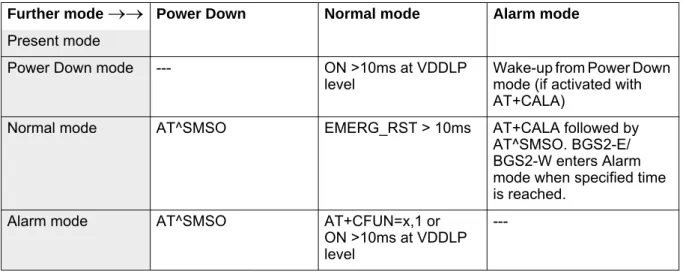
Further mode
Power Down Normal mode Alarm modePresent mode
Power Down mode --- ON >10ms at VDDLP
level Wake-up from Power Down mode (if activated with AT+CALA)
Normal mode AT^SMSO EMERG_RST > 10ms AT+CALA followed by AT^SMSO. BGS2-E/ BGS2-W enters Alarm mode when specified time is reached.
Alarm mode AT^SMSO AT+CFUN=x,1 or
ON >10ms at VDDLP level
---3.7
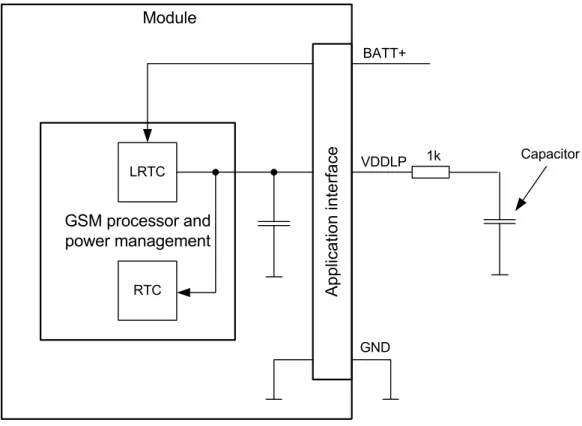
RTC Backup
The internal Real Time Clock of BGS2-E/BGS2-W is supplied from a separate voltage regulator in the power supply component which is also active when BGS2-E/BGS2-W is in Power Down mode and BATT+ is available. An alarm function is provided that allows to wake up BGS2-E/ BGS2-W without logging on to the GSM network.
In addition, you can use the VDDLP pad to backup the RTC from an external capacitor. The capacitor is charged from the internal LDO of BGS2-E/BGS2-W. If the voltage supply at BATT+ is disconnected the RTC can be powered by the capacitor. The size of the capacitor determines the duration of buffering when no voltage is applied to BGS2-E/BGS2-W, i.e. the greater the capacitor the longer BGS2-E/BGS2-W will save the date and time. The RTC can also be sup-plied from an external battery (rechargeable or non-chargeable). In this case the electrical specification of the VDDLP pad (see Section 5.4) has to be taken in to account.
Figure 12 shows an RTC backup configuration.
Figure 12: RTC supply variants
Capacitor VDDLP GSM processor and power management LRTC RTC Ap pl ic at io n inte rfa ce BATT+ Module 1k GND
3.8
SIM/USIM Interface
The baseband processor has an integrated SIM/USIM card interface compatible with the ISO/ IEC 7816 IC Card standard. This is wired to the host interface in order to be connected to an external SIM card holder. Five pads are reserved for the SIM interface. BGS2-E/BGS2-W sup-ports and automatically detects 3.0V as well as 1.8V SIM cards.
The CCIN pad serves to detect whether a tray is present in the card holder. Using the CCIN pad is mandatory for compliance with the 3GPP TS 11.11 (Rel.99) recommendation if the me-chanical design of the host application allows the user to remove the SIM card during operation.
The figure below shows a circuit to connect an external SIM card holder.
Table 12: Signals of the SIM interface (SMT application interface)
Signal Description
CCCLK Chipcard clock, various clock rates can be set in the baseband processor. CCVCC SIM supply voltage from PSU-ASIC
CCIO Serial data line, input and output.
CCRST Chipcard reset, provided by baseband processor
CCIN Input on the baseband processor for detecting a SIM card tray in the holder.The default level of CCIN is low (internal pull down resistor, no card inserted). It will change to high level when the card is inserted. To take advantage of this feature, an appropriate contact is required on the cardholder. Ensure that the cardholder on your application platform is wired to output a high signal when the SIM card is present.
The CCIN pad is mandatory for applications that allow the user to remove the SIM card dur-ing operation.
The CCIN pad is solely intended for use with a SIM card. It must not be used for any other purposes. Failure to comply with this requirement may invalidate the type approval of BGS2-E/BGS2-W. SIM CCVCC CCRST CCIO CCCLK 220nF 1nF CCIN V180 4k 7
It is recommended that the total cable length between SMT application interface pads on BGS2-E/BGS2-W and the connector of the external SIM card holder must not exceed 100mm in order to meet the specifications of 3GPP TS 51.010-1 and to satisfy the requirements of EMC compliance.
To avoid possible cross-talk from the CCCLK signal to the CCIO signal be careful that both lines are not placed closely next to each other. A useful approach would be to use a separate SIM card ground connection to shield the CCIO line from the CCCLK line. A GND line may be employed for such a case.
Notes: No guarantee can be given, nor any liability accepted, if loss of data is encountered after removing the SIM card during operation.
Also, no guarantee can be given for properly initialising any SIM card that the user inserts after having removed a SIM card during operation. In this case, the application must restart BGS2-E/BGS2-W.
If using a SIM card holder without detecting contact please be sure to switch off the module before removing the SIM Card or inserting a new one.
3.9
Serial Interface ASC0
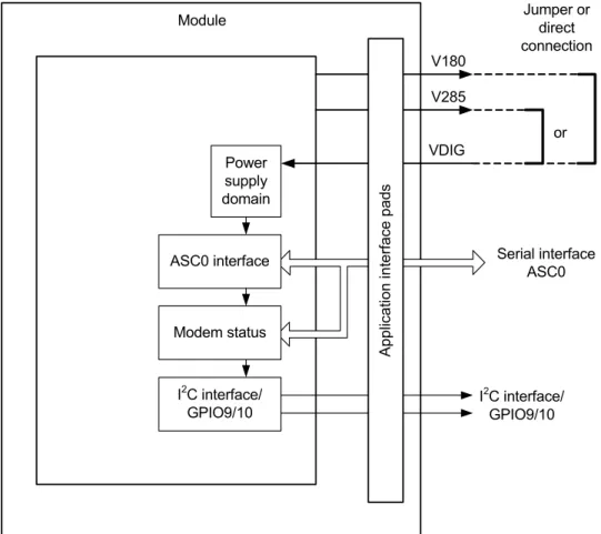
BGS2-E/BGS2-W offers an 8-wire unbalanced, asynchronous modem interface ASC0 con-forming to ITU-T V.24 protocol DCE signalling. The electrical characteristics do not comply with ITU-T V.28. The voltage level of the ASC0 interface can be configured to either 1.8V or 2.85V: • If the VDIG signal (i.e., application interface pad 10) is connected to the V180 line (i.e.,
application interface pad 35) the ASC0 interface starts up with a 1.8V signal level.
• If the VDIG signal (i.e., application interface pad 10) is connected to the V285 line (i.e., application interface pad 22), the ASC0 interface runs with a 2.85V signal level.
The voltage level configuration of the ASC0 interface also has an impact on the I2C interface. The I2C interface is also in the power supply domain configured by the VDIG signal (see Sec-tion 3.13).
For electrical characteristics of the interface signals please refer to Section 5.4.
Figure 14: VDIG controlled power supply domain
BGS2-E/BGS2-W is designed for use as a DCE. Based on the conventions for DCE-DTE con-nections it communicates with the customer application (DTE) using the following signals: • Port TXD @ application sends data to the module’s TXD0 signal line
• Port RXD @ application receives data from the module’s RXD0 signal line
ASC0 interface Modem status Power supply domain Module I2C interface/ GPIO9/10 Application interf ace pad s V180 V285 Serial interface ASC0 I2C interface/ GPIO9/10 or VDIG Jumper or direct connection