Power efficient adaptive mitigation of local interference in
multimode wireless transceivers
Citation for published version (APA):
Habibi, H. (2014). Power efficient adaptive mitigation of local interference in multimode wireless transceivers. Technische Universiteit Eindhoven. https://doi.org/10.6100/IR770338
DOI:
10.6100/IR770338
Document status and date: Published: 13/03/2014 Document Version:
Publisher’s PDF, also known as Version of Record (includes final page, issue and volume numbers) Please check the document version of this publication:
• A submitted manuscript is the version of the article upon submission and before peer-review. There can be important differences between the submitted version and the official published version of record. People interested in the research are advised to contact the author for the final version of the publication, or visit the DOI to the publisher's website.
• The final author version and the galley proof are versions of the publication after peer review.
• The final published version features the final layout of the paper including the volume, issue and page numbers.
Link to publication
General rights
Copyright and moral rights for the publications made accessible in the public portal are retained by the authors and/or other copyright owners and it is a condition of accessing publications that users recognise and abide by the legal requirements associated with these rights. • Users may download and print one copy of any publication from the public portal for the purpose of private study or research. • You may not further distribute the material or use it for any profit-making activity or commercial gain
• You may freely distribute the URL identifying the publication in the public portal.
If the publication is distributed under the terms of Article 25fa of the Dutch Copyright Act, indicated by the “Taverne” license above, please follow below link for the End User Agreement:
www.tue.nl/taverne
Take down policy
If you believe that this document breaches copyright please contact us at:
providing details and we will investigate your claim.
Power efficient adaptive mitigation
of local interference
in multimode wireless transceivers
proefschrift
ter verkrijging van de graad van doctor aan de Technische
Universiteit Eindhoven, op gezag van de rector magnificus
prof.dr.ir. C.J. van Duijn, voor een commissie aangewezen
door het College voor Promoties, in het openbaar te
verdedigen op donderdag 13 maart 2014 om 16:00 uur
door
Hooman Habibi
voorzitter: prof.dr. H. Corporaal 1e promotor: prof.dr.ir. J.W.M. Bergmans 2e promotor: prof.dr.ir. P.G.M. Baltus
copromotor: dr. Y. Wu
leden: prof.dr.ir. B. Nauta (University of Twente) prof.dr.Ing G. Ascheid (RWTH Aachen) prof.dr.ir. E.R. Fledderus
To Sophie, Negar, and my parents.
Power efficient adaptive mitigation of local interference in multimode wireless transceivers / by Hooman Habibi – Eindhoven University of Technology, Eind-hoven, The Netherlands, 2014
©2014 Hooman Habibi
All rights reserved. No part of this publication may be reproduced, stored in a retrieval system, or transmitted, in any form or by any means, electronic, mechan-ical, photocopying, recording or otherwise, without the prior written permission from the copyright owner.
A catalogue record is available from the Eindhoven University of Technology Li-brary
ISBN: 978-90-386-3579-8 NUR 959
Subject headings: Multimode transceivers, Multiradio coexistence, Interference mitigation, Adaptive systems, Adaptive circuits, Nonlinear circuits.
This thesis was prepared with the LATEX documentation system. Cover design:Paul Verspaget
v
Summary
Nowadays, handheld devices like mobile phones and tablets have become widespread. These devices support several wireless communication standards for various func-tionalities, e.g. voice and video calls, data transfer, and location finding. The collection of several transceivers in one device, which is required to implement these standards, is referred to as a multimode transceiver.
It is often required that two standards are used simultaneously in one multimode transceiver. Owing to the small size of the transceiver, a local transmitter for one standard induces a strong interference in the local receiver for the other standard, often many orders of magnitude stronger than the desired signal of the receiver. If the strong interference is not suppressed at an early stage of the receiver front-end, it will induce nonlinear distortion products and may cause a severe loss of receiver sensitivity, called desensitization. State of the art approaches to sufficiently sup-press the interference require unpractical power consumption or analogue com-plexity. Hence they are not suitable for application in handheld devices.
In this thesis we study a novel hybrid approach, which combines mixed-signal cir-cuits and digital signal processing techniques, to mitigate the local interference with low complexity and power consumption. The approach uses a memoryless Nonlinear Interference Suppressor (NIS) in the receiver front-end to significantly suppress the local interference and prevent desensitization. Design of this mixed-signal circuit is discussed in a companion PhD thesis [1]. For the NIS to suppress the interference, it must be dynamically adapted to accurately track the interfer-ence envelope. In this thesis we exploit the local availability of an interferinterfer-ence reference to devise simple yet accurate digital NIS adaptation schemes.
Successful design and implementation of our approach is carried out in three stages. Firstly, based on ideal models we perform a system study, which shows the benefits and drawbacks of using the NIS. Secondly, accuracy requirements for the adapta-tion signal of the NIS are derived and a closed-loop adaptaadapta-tion method is designed to meet these requirements. Thirdly, the NIS circuit is integrated in a test bed transceiver, the ideal models are revised based on measurements, and adaptation methods are refined based on the revised models. Predictable and successful op-eration of the test bed validates the presented analysis and simulations.
When the combination of the strong interference and the weak desired signal ex-periences any nonlinearities in the receiver front-end, distortion products are gen-erated. One of these is Cross-Modulation (CM) distortion, where the amplitude modulation of the interference transfers to modulation of the desired signal. CM distortion is particularly problematic, since it occurs independent of the frequency
separation of the desired signal and the interference. In this thesis we encounter CM distortion in two situations, namely without and with NIS. The first situation is of interest since the interference can be weak enough to be handled without NIS yet strong enough to cause CM distortion. In this situation the CM distortion can be compensated digitally. In Chapter 2, we propose a simple digital compensation method that exploits the local availability of the baseband interference to avoid the complexity and power dissipation of additional analogue circuits.
In Chapter 3, we introduce the NIS and study its potential benefits. Firstly, we derive an optimal adaptation signal for the NIS that yields complete suppression of the interference in the absence of the desired signal. For this optimal adaptation signal, residual distortion products of the NIS are identified. The impact of these products on the received desired signal is analyzed and rules of thumb are given to specify conditions for which adequate interference suppression is combined with negligible distortion. We show that these conditions are met in most cases of practical interest.
The optimal adaptation signal is proportional to the envelope of the received interference at the NIS input. A key feature in the multimode transceiver is the local availability of the interference source. Using a baseband linear model of the interference coupling path, from the local transmitter to the local receiver, the adaptation signal can be obtained digitally. In Chapter 4, we quantify the required accuracy for the adaptation signal to properly suppress the interference while keeping the degradation of the receiver Symbol Error Rate (SER) negligible. To provide the required accuracy, we propose a closed-loop method to dynamically adapt the path model such that the power of the residual interference at the output of the NIS is minimized. This method uses the baseband interference as a reference to combine simplicity with high accuracy and high speed. Our analysis and simulations show that the optimal adaptation signal can be estimated with sufficient accuracy, such that the interference is strongly suppressed while a SER close to that of an exactly linear receiver is achieved.
In Chapters 3 and 4, idealized models of the NIS and adaptation circuits are used to analyze the performance afforded by the NIS. In Chapter 5, we present ex-perimental results of a multimode transceiver test bed that uses the mixed-signal integrated NIS circuit designed in [1]. The main circuit imperfections that limit the NIS performance are identified and simple imperfection models are described that explain the experimental results. Based on these models, the NIS adaptation method is extended with simple digital compensation and calibration techniques that unlock the full interference suppression potential of the NIS circuit. Fur-thermore, a low-complexity digital compensation method is proposed for the CM distortion that is caused by the imperfections. Successful operation of the test bed suggests that the NIS approach is practical and attractive for multimode transceivers.
vii
Concluding remarks and suggestions for future work are collected in Chapter 6. The analysis, simulation and experimental results in this thesis show that the NIS can achieve substantial interference suppression at attractive complexity and power dissipation, and that the residual distortion products can be digitally compensated with a low complexity. Both fundamental and practical limitations of the proposed approach are identified, and directions for future improvements are sketched. References:
[1] Ph.D. Thesis E.J.G. Janssen, ”Methodologies for Multi-Radio Coexistence; Self-Interference Suppression Techniques”.
Contents
Summary v
Contents vii
List of Abbreviations xiii
List of Symbols xv
1 Introduction 1
1.1 Wireless technologies in handheld devices . . . 1
1.2 Local interference in local receiver . . . 3
1.2.1 Receiver model . . . 3
1.2.2 Interference classification . . . 4
1.2.3 Impact of a strong interference on the received signal . . . . 5
1.3 State of the art in interference mitigation . . . 7
1.3.1 Time division multiplexing . . . 7
1.3.2 Linear filtering . . . 8
1.3.3 Analogue cancellation of interference . . . 8
1.3.4 Digital compensation . . . 10
1.4 Proposed hybrid approach . . . 10
1.4.1 Nonlinear Interference Suppressor . . . 11
1.4.2 Digital compensation of CM distortion . . . 12
1.4.3 Other areas of application for the NIS . . . 13
1.5 Outline and contribution of this thesis . . . 14
1.6 Publications . . . 15
1.6.1 Journal publications . . . 15
1.6.2 Conference proceedings . . . 16
Appendix I:Single-branch analogue cancellation . . . 18
2 Digital Compensation of Cross-Modulation Distortion 25 2.1 Abstract . . . 25
2.2 Introduction . . . 26
2.3.1 Derivation of the LNA input . . . 30
2.3.2 Derivation of analog baseband signal . . . 31
2.3.3 Derivation of discrete-time received signal . . . 33
2.4 Proposed compensation method . . . 34
2.4.1 Estimation ofτi . . . 34
2.4.2 Estimation ofc . . . 35
2.5 Simulation results . . . 37
2.5.1 Accuracy of ˆτi . . . 38
2.5.2 Accuracy of ˆc . . . 39
2.5.3 SER performance of the compensation scheme . . . 41
2.6 Conclusion . . . 43
Appendix I: Estimation ofτ . . . 44
Appendix II: Proof for variance of ˆc . . . 45
3 System Study on Nonlinear Suppression of Varying-Envelope In-terference 49 3.1 abstract . . . 49
3.2 Introduction . . . 50
3.2.1 Interference suppression by linear filtering . . . 51
3.2.2 Interference cancellation . . . 51
3.2.3 Nonlinear interference suppression . . . 52
3.2.4 Adaptive nonlinear interference suppression . . . 53
3.3 System model . . . 55
3.3.1 The received signal after the BPF . . . 55
3.3.2 baseline receiver . . . 56
3.3.3 Receiver with NIS . . . 57
3.4 Nonlinear interference suppressor . . . 57
3.4.1 NIS modeling and adaptation . . . 57
3.4.2 NIS output in the presence of the desired signal . . . 58
3.4.3 Gain Variation Distortion . . . 61
3.4.3.1 Case 1: constant-envelope interference and OFDM desired signal . . . 62
3.4.3.2 Case 2: OFDM interfering and desired signals . . 63
3.4.4 IM leakage . . . 64
3.4.5 Effect of input channel noise on the receiver with NIS . . . 64
3.5 Simulation Results . . . 65
3.5.1 Evaluation of IM leakage . . . 65
3.5.2 SER comparison of the baseline RX and the RX with NIS . 66 3.5.2.1 SER performance for constant-envelope interfer-ence and OFDM desired signal . . . 67
3.5.2.2 SER performance for OFDM modulated desired signal and OFDM interference . . . 68
3.5.3 Comparison of the required number of ADC bits . . . 70
3.6 Conclusion . . . 71
Contents xi
Appendix II: Proof for dependence of envelopes on ISIR . . . 74
Appendix III: Proof for calculation of SDR . . . 75
4 Closed-loop Adaptation of a Nonlinear Interference Suppressor 77 4.1 abstract . . . 77
4.2 Introduction . . . 78
4.3 System model . . . 80
4.3.1 Description of the signals received by the local RX . . . 80
4.3.2 Adaptation signal . . . 82
4.3.3 Description of the signals at the NIS output . . . 83
4.3.3.1 Interference suppression . . . 84
4.3.3.2 Distortion products . . . 84
4.3.4 External interference . . . 85
4.4 Accuracy requirements for NIS adaptation . . . 86
4.4.1 Impact of adaptation signal errors on the NIS performance 87 4.4.2 Linear model of the TX-RX path . . . 89
4.4.3 Accuracy requirements of filter tapsgn. . . 90
4.4.4 Required number of filter taps for modelling the SAW filter 90 4.5 Closed-loop adaptation of the NIS . . . 92
4.5.1 Extraction of error signal . . . 93
4.5.2 adaptation algorithm . . . 93
4.5.3 Convergence of the adaptation algorithms . . . 95
4.5.4 Speed of the adaptation loop . . . 95
4.6 Simulation Results . . . 97
4.6.1 Simulation setup . . . 97
4.6.2 Interference suppression . . . 98
4.6.3 Distortion products and SER of the RX . . . 98
4.6.4 External Interference . . . 101
4.7 Implementation aspects of the adaptation loop . . . 102
4.7.1 Conversion rate of the DAC . . . 102
4.7.2 Number of DAC and ADC bits . . . 102
4.7.3 Power consumption of the NIS approach . . . 103
4.8 Conclusion . . . 103
Appendix I : Possible Solutions for filter taphn . . . 105
Appendix II: Derivation of the error signal . . . 108
Appendix III: Derivation of the gradient . . . 110
5 Experimental evaluation of an Adaptive Nonlinear Interference Suppressor 113 5.1 abstract . . . 113
5.2 Introduction . . . 114
5.3 System model . . . 116
5.3.1 Multimode Transceiver with NIS . . . 116
5.3.2 Adaption of the NIS . . . 118
5.5 Measurement and analysis for Single Tone (ST) signals . . . 121
5.5.1 Adaptation Signal . . . 121
5.5.2 Phase Misalignment Between Amplifier and Limiter . . . . 122
5.5.3 Measurements ofgiandgdin the presence of the desired signal123 5.5.4 AM-PM distortion . . . 124
5.5.5 Characteristics of the switching mixer . . . 125
5.5.6 DC Offset of the switching mixer . . . 126
5.5.7 Closed-loop adaptation for varying-envelope interferences . 128 5.6 Measurement results for constant-envelope interference . . . 128
5.7 Analysis and measurement results for varying envelope interferences 129 5.7.1 Numerical results . . . 130
5.7.2 Measurement results for closed-loop adaptation . . . 132
5.7.3 Digital compensation of distortion . . . 133
5.7.4 Real time adaptation . . . 135
5.7.5 Calibration . . . 136
5.7.6 Power consumption of the NIS approach . . . 136
5.8 Comparison and summary . . . 137
5.8.1 Comparison to analogue cancellation . . . 137
5.8.2 Strengths and Weaknesses of the NIS . . . 139
5.9 Conclusion . . . 140
6 Conclusions and future work 143 6.1 Conclusions . . . 143
6.1.1 Digital compensation of Cross-Modulation (CM) . . . 145
6.1.2 Nonlinear interference suppressor, Principle of operation . . 146
6.1.3 Nonlinear interference suppressor, closed loop adaptation . 146 6.1.4 Nonlinear interference suppressor, Experimental results . . 147
6.2 Future work . . . 148
6.2.1 Improvements and explorations for the NIS . . . 148
6.2.2 Improving the digital compensation method . . . 149
6.2.3 Application of the NIS for FMCW radar . . . 150
6.2.4 Application of the NIS for RFID readers . . . 150
Bibliography 151
Acknowledgement 159
xiii
List of Abbreviations
ADC Analogue to Digital Converter
AGC Automatic Gain Controller
AWGN Additive White Gaussian Noise
BPF Band Pass Filter
CDMA Code Division Multiple Access
CM Cross-Modulation
CSCG Circularly-Symmetric Complex Gaussian
DAC Digital to Analogue Converter
DFT Discrete Fourier Transform
FE Front-End
FIR Finite Impulse Response
FMCW Frequency Modulated Continuous Wave
FPGA Field Programmable Gate Array
GMSK Gaussian Minimum Shift Keying
GNSS Global Navigation Satellite System
GPS Global Positioning System
GSM Global System for Mobile communication
GVD Gain Variation Distortion
IM Inter-Modulation
IIP3 Input third-order Intercept Point
IM3 third-order Intermodulation
LO Local Oscillator
LPF Low Pass Filter
LNA Low Noise Amplifier
LRX Local Receiver
LTX Local Transmitter
LTE Long Term Evolution for wireless communica-tion
MBPS Mega Bit Per Second
MER Modulation Error Ratio
MSPS Mega Symbol Per Second
MSE Mean Square Error
MMSE Minimum Mean Square Error
NAE Normalized Adaptation Error
NIS Nonlinear Interference Suppressor
OFDM Orthogonal Frequency division Multiplexing
P1dB 1dB Compression Point
PAPR Peak to Average Power Ratio
PSD Power Spectral Density
QAM Quadrature Amplitude Modulation
RF Radio Frequency
RFID Radio Frequency Identification
RX Receiver
RTX Remote Transmitter
SAW Surface Acoustic Wave
SER Symbol Error Rate
SDR Signal to Distortion Ratio
SIMR Signal to Inter-Modulation Ratio
SIR Signal to Interference Ratio
SNR Signal to Noise Ratio
SRCD Sampling Rate Conversion and Delay block
TX Transmitter
TRX Transceiver
VSG Vector Signal Generator
WiMax Worldwide Interpretability for Microwave
Ac-cess
xv
List of Symbols
Ai Envelope of the interference Ad Envelope of the desired signal
Ai,y Envelope of the interference at the Nonlinear Interference Suppressor (NIS) output
Ad,y Envelope of the desired signal at the NIS out-put
AIM Envelope of the third-order intermodulation at the NIS output
Bi Bandwidth of the interference Bd Bandwidth of the desired signal d[n] Baseband discrete-time desired signal
∆f Frequency separation between interference and the desired signal
E() Expected value
fi Frequency of the interference fd Frequency of the desired signal ϕi(t) Phase of the interference ϕd(t) Phase of the desired signal
g[n] Estimated baseband equivalent impulse re-sponse of interference coupling path
gi Gain of a block for the interference gd Gain of a block for the desired signal
h Baseband equivalent impulse response of in-terference coupling path
i[n] Baseband discrete-time interference l(t) Adaptation signal of the NIS ˜
l(t) Optimal adaptation signal ˆ
l(t) Estimated adaptation signal
Pi(t) Instantaneous power of the interference at NIS input
Pd(t) Instantaneous power of the desired signal at NIS input
Pi Average power of the interference at NIS input Pd Average power of the desired signal at NIS
in-put
x(t) NIS input signal y(t) NIS Output signal
z(t) Signal received by the local receiver at the input of the Analogue to Digital Con-verter(ADC)
z[n] Signal received by the local receiver at the out-put of the ADC
Chapter 1
Introduction
Nowadays, handheld devices like mobile phones and tablets have become widespread. These devices support several wireless communication standards for various func-tionalities, e.g. voice and video calls, data transfer, location finding. To enable these standards a number of transceivers is required(a transceiver is a pair of a transmitter and a receiver.) The collection of these transceivers in one device is re-ferred to as a multimode transceiver. In this chapter, we first describe the problem of a strong local interference, which is encountered in multimode transceivers when a local transmitter and a local receiver are active simultaneously in the same hand-held device. State of the art approaches to handle this problem are explored. It is concluded that these approaches are not adequate as they require an unpractical power consumption or are not suitable for application in handheld devices. Then the proposed solution for mitigation of the local interference is discussed. This solution uses an adaptive memoryless nonlinearity to suppress the interference at an early stage of the receiver front-end and uses digital signal processing tech-niques for its adaptation and for compensation of nonlinear distortion products, which are caused by application of this nonlinearity in the receiver. The chapter concludes by describing the outline and contributions in the following chapters of this thesis.
1.1
Wireless technologies in handheld devices
With the first handheld mobile device introduced in 1973 it became possible to make phone calls with a device portable by a human, without being restricted by wires. From then to this day, handheld devices, including phones and tablets,
have changed dramatically to provide more functionalities. Beside their origi-nal purpose, i.e. voice communication, nowadays handheld devices offer wireless connectivity for a vast range of applications, with using a variety of communica-tion standards. Short-range communicacommunica-tion for transfer of data and conneccommunica-tion to peripherals, near field communication for electronic wallet, Global Navigation Satellite System (GNSS) for navigation, and cellular long-range communication for transfer of voice and data over wide areas can be mentioned. The weight and size of these devices have been reduced to about 100 grams and the size of a palm of a hand.
To implement every communication standard a wireless transceiver is required. The inside of a modern mobile phone is shown in Fig. 1.1. Several transceivers (cellular transceiver, GNSS, WLAN and Bluetooth), are gathered in one small device to implement each of the standards. From the users’ point of view, the si-multaneous operation of these transceivers is highly desirable. For example during a phone call through a cellular network, the user may want to use a Bluetooth handsfree, he may want to acquire his position through GNSS, or look at his agenda stored in an online server. The combination of several transceivers, which is called a multimode transceiver, is required to implement these standards. The mobility requirement necessities the handheld devices to rely on batteries as the energy source. The current trend shows that the power consumption of all devices is increasing faster than the capacity of the batteries. Hence minimizing the power consumption of the transceivers is of the utmost importance.
Fig. 1.2 shows a sample multimode transceiver in operation. The figure includes a Remote Transmitter (RTX), a Local Receiver (LRX), a Local Transmitter (LTX), and a remote receiver. The LRX and RTX belong to one communication standard and the LTX the remote receiver to another one. The RTX transmits a signal, shown in blue, which is received by the LRX antenna as the received desired signal, after propagation losses. At the same time the LTX transmits a signal, shown in red, to be received by the remote receiver. The LTX signal is partly received by the LRX antenna after a coupling loss, and induces a local interference. The distance between the LTX and LRX is dictated by the size of the handheld device and is typically a few centimeters. On the other hand the distance of the RTX and LRX can range from a few meters to a few kilometers. The propagation loss between a transmitter and receiver is proportional to the square of the distance between them. Hence the received signal by the LRX includes an interference which can be many orders of magnitude stronger than the desired received signal. The high level of this local interference compared to that of the desired signal is one of the main challenges in the implementation of a multimode transceiver. Owing to the extreme proximity of the LTX and LRX, the local interference is much stronger than interferences received from other devices, i.e. external interferences. Current techniques for mitigation of external interferences are not able to handle the local interference, thus severely limiting simultaneous operation. In the next section,
1.2 Local interference in local receiver 3
Figure 1.1: Inside view of a mobile phone.
5HPRWH WUDQVPLWWHU
0XOWLPRGH WUDQVFHLYHU
5HPRWH UHFHLYHU /RFDO
UHFHLYHU
/RFDO WUDQVPLWWHU
Figure 1.2: A multimode transceiver in operation.
we describe the impact of this strong interference on the LRX.
1.2
Local interference in local receiver
1.2.1
Receiver model
Fig. 1.3 shows a direct conversion receiver, which is a popular architecture for modern receiver design. Here in-phase and quadrature signals are shown with double lines. The combination of the desired signal and the interference is received by an antenna. The power spectral density of the received signal is shown and includes the desired signal and the local interference with center frequencies fd
;
%3) /1$
/2
$'&
'LJLWDO %DVHEDQG SURFHVVRU /3)
L
I
GI
Figure 1.3: Direct conversion receiver
and fi, respectively. The received signal is passed through a Band Pass Filter (BPF), which selects a frequency band of interest. The filtered signal is amplified by a Low Noise Amplifier (LNA) and is down-converted using a quadrature mixer, which is excited with a Local Oscillator (LO) that is locked to fd. To select the frequency channel of the desired signal, the analogue baseband signal is filtered by a Low Pass Filter (LPF), and sampled and digitized by an Analogue to Digital Converter (ADC). Additional filtering and extracting the symbols transmitted by the RTX is performed in the digital baseband processor.
1.2.2
Interference classification
Three distinct scenarios can be considered based on the center frequency of the interference:
1-Co-channel interference: The interference is in the frequency channel of the desired signal. This is the most disruptive scenario and is generally prevented during standardization. Hence in this thesis we do not consider this scenario, and assume that the local interference and the desired signal do not have any spectral overlap.
2-Co-band interference: The interference is in the frequency band of the desired signal, although it is not co-channel. Typically, the co-band interference belongs to the same standard as the desired signal and it is an external interference. There are, however, cases like Bluetooth and WLAN that two standards share a frequency band and their simultaneous operation in one device is desired. Hence the co-band scenarios have some degree of importance for multimode operation. The BPF has no impact on the co-band interference and the receiver relies on low-pass filtering after down-conversion to filter out the interference.
3-Out-of-band interference: The interference is not in the band of the desired signal. This is the most common scenario for multimode operation. An out-of-band interference is suppressed by the BPF to some extent. Complete filtering of the interference is performed after down-conversion by the LPF or digital filters
1.2 Local interference in local receiver 5
L
$
GJ
Figure 1.4: Input-output characteristics and weak signal gain versus envelope of a strong interference for a typical active component in the receiver FE
after the ADC.
1.2.3
Impact of a strong interference on the received signal
In principle, an interference which is not co-channel, can be completely suppressed by linear filtering. The BPF is meant to suppress the out-of-band interference. With the current technology, however, even after the BPF, the local interference can still be many orders of magnitude stronger than the desired signal. More-over, the BPF becomes ineffective for a co-band interference or an interference in the transition band of the BPF. If the receiver Front-End (FE) is linear then the interference can be suppressed after down-conversion by the LPF or digital filter-ing. Active components of the FE, however, are linear only for a limited range of inputs. As shown in Fig. 1.4 a, the output eventually saturates as the input increases. Such a nonlinear IO characteristic leads to several undesirable effects:E1-Desensitization: As the envelope Ai of the interference increases, the gain
gd of the weak desired signal decreases as shown in Fig. 1.4b, and eventually approaches zero. This excessive loss of gain leads to sensitivity loss of the receiver and is called desensitization [1]. Desensitization occurs for all interference scenarios in Section 1.2.2.
E2-Cross-Modulation (CM) distortion: It is seen in Fig. 1.4 b that there is
a region where gd depends on Ai. For a varying-envelope interference, variation of Ai(t) leads to a variation of gd(Ai). Hence the modulation of the interference transfers to the modulation of the desired signal and leads to distortion of the desired signal. This form of distortion is called cross-modulation distortion. CM distortion occurs for all interference scenarios in Section 1.2.2.
E3-Third-order intermodulation (IM3) product: Suppose that, as shown
in Fig. 1.5, besides the local interference an external interference with a center frequency fe is present at the input of a nonlinear block with the characteristic
I L
I H
I IH IL IL−IH I
,QSXW 2XWSXW
Figure 1.5: Generation of the IM3.
shown in Fig. 1.4. At the output of the block the third-order intermodulation (IM3) product of these two signals appears with a center frequency of 2fi−fe. The power of this IM3 product approaches the power of the external interference as the local interference becomes stronger. The IM3 product can fall into the frequency channel of the desired signal, if fe is close to 2fi−fd. For out-of-band interference scenarios, fe will be further out-of-band. Hence this effect is considerable only for co-band interference.
E4-Spectral growth of the interference: As the interference passes through
the LRX nonlinear blocks, nonlinear distortion products of the interference are generated. The bandwidth of these products can be larger than the bandwidthBi of the interference. If the frequency separation between the interference and the desired signal is small then these products can fall into the frequency channel of the desired signal. Hence this effect can only be considerable for co-band interference scenarios.
Besides the above effects, the following items can also affect the LRX reception. They originate from the LTX imperfections and the large coupling between the LTX and the LRX. Hence they will be present even for an exactly linear LRX FE.
E5-Amplified LTX noise: The LTX frond-end up-converts the baseband
inter-ference, amplifies and transmits it. At the same time the thermal noise at the input of the LTX front-end is amplified and is transmitted. Typically a bandpass filter is used before the LTX antenna to suppress the amplified noise and harmon-ics of the interference. For the co-band interference however, this bandpass filter has no effect. If the coupling between the LTX and LRX is large, the LTX noise can significantly affect the desired signal.
E6-Spectral growth of the interference in the LTX power amplifier:
Sim-ilar to E4, owing to nonlinearity of the LTX Power Amplifier (PA), nonlinear products of the interference are generated. Similar to E4 this effect can only be considerable for co-band interference scenarios.
The above undesirable effects can severely disrupt the LRX reception. In the next section we look at state of the art approaches for mitigation of these effects. Since
1.3 State of the art in interference mitigation 7
E1,2 affects the received signal for all interference scenarios, the main focus of our work is on the mitigation of these two effects.
1.3
State of the art in interference mitigation
There are several approaches to mitigate the local interference. 1. It can be avoided by time multiplexing.
2. It can be suppressed in the analogue domain by linear filtering or by a nonlinearity as we will see in the next section.
3. It can be cancelled in the analogue domain by generating and subtracting a replica of the interference.
4. It can be filtered, cancelled, or its effect on the desired signal can be com-pensated in the digital domain.
Except for the first approach, these approaches are not mutually exclusive and may need to be combined to successfully mitigate the local interference. The digital mitigation approach is mainly a complementary approach and cannot mitigate desensitization. In this section we explore the above approaches, as found in the state of the art.
1.3.1
Time division multiplexing
The two conflicting standards can be time division multiplexed such that the RTX and LTX do not transmit at the same time. Such an approach is proposed in [2] to enable coexistence between Bluetooth and WLAN and in [3] to enable coexistence between LTE and Bluetooth, WLAN, and GNSS. This approach has two limitations:
1- it requires cooperation between two communication standards which is complex and is not yet a part of many standards,
2- it reduces the throughput of each standard by necessitating extra signaling and guard times.
1.3.2
Linear filtering
One may attempt to increase the dynamic range of the LRX FE to prevent E1-4, so that the LPF can suppress the interference. Unfortunately, to strongly increase the dynamic range for a certain technology and circuit topology, the power con-sumption of the FE circuits must be strongly increased [4]. Increasing the power consumption is highly undesirable, considering the limited energy supply of hand-held devices.
1.3.3
Analogue cancellation of interference
By subtracting a replica of the received interference from the received signal, the interference can be cancelled while the desired signal remains unaffected. In prin-ciple, the cancellation can be done in the analogue or the digital domain. Digital cancellation, however, is not effective in mitigation of E1-6. Hence the cancellation must be done in an early stage of the LRX FE.
In multimode transceivers the received local interference originates from the locally known transmitted interference. The knowledge of the transmitted interference can be exploited for mitigation of the received interference. As shown in Fig. 1.6, a replica of the received interference at the LRX can be generated based on a linear model of the interference coupling path, shown with a bold line, and the transmitted interference as the input of this model. By subtracting this replica from the received signal in the analogue domain the local interference can be cancelled. The subtraction point in Fig. 1.6, is preferred to be before the active components of the LRX FE, i.e. after the LRX antenna or the BPF. Subtraction after the LNA however, may be explored with an aim to reduce the impact of added noise by cancellation [5]. If an exact model of the coupling path can be constructed this method can resolve E1-6. For this reason, this method is widely explored [5–10].
It must be considered that mitigation of E1-4 and E5-6 requires cancellation over both the frequency channels of the interference and desired signal, respectively. Hence the path model must be accurate over both frequency channels, otherwise mitigation of E1-4 may lead to aggravation of E5-6, or the other way around. Providing such an accuracy becomes more difficult as frequency separationfi−fd between the desired signal and interference, or their bandwidths, increase. The interference coupling path is subject to environmental changes. For exam-ple, the presence and movement of a user’s hand changes the characteristics of the coupling path. Hence the path model should be adaptive. Such an adap-tive model is shown in Fig. 1.7, where ai are adaptable complex gains andτi are
1.3 State of the art in interference mitigation 9
/7; )(
%DVHEDQG LQWHUIHUHQFH
/7; /5;
0RGHORI LQWUISDWK
Figure 1.6: Analogue cancellation of the local interference
*DLQ 'HOD\
τ
D
*DLQ 'HOD\
Q
τ
Q
D
#
$QDORJXHPRGHO
/7; /5;
Figure 1.7: Adaptive analogue model
fixed delays. Our study in Appendix I shows that for wideband interferences, a multi-path model is required to achieve an adequate interference cancellation. In practice, however, even a single-path model requires a significant analog complex-ity and power consumption. In particular, implementing long delays (in the order of several nanoseconds) in an integrated circuit can be difficult. Hence in [5,7,9,10] only a single-path model without a delay element is implemented which suffices only to cancel the interference in a very narrow band. To improve the interference cancellation in [7] and [10], the coupling path is emulated using a bandpass filter or the input of the model is collected by an antenna similar to the LRX antenna. These two methods, however, are not suitable for mobile devices as they require more external components and also are not flexible (must be physically modified for each design).
In [11] the performance of a single-path model without delay or emulating the cou-pling path is studied. The interference is suppressed by only 10-20 dB, depending on the bandwidth of the interference. Such a single-path model not only fails to
suppress the interference such that E1-4 are prevented, it even aggravates E4-5, since the model is not accurate enough over frequency channel of the interference nor that of the desired signal. A multipath (2-path) model approach is proposed in [6] to achieve cancellation at both fi andfd. The complexity and cost of such a multipath model makes it unsuitable for handheld devices.
Another limitation of the analog cancellation method is difficulty of its adaptation. For a reference-aided adaptation, analog circuits must be implemented to correlate the transmitted interference with the residual interference after the cancellation point [5]. Such an adaptation would increase the complexity further. Hence in [7] a search method overa1is used to minimize the energy of the residual interference. Such a search method, however, becomes increasingly slow when the number of paths increases.
Let us assume that an exact model of the coupling path can be constructed. For such an exact model E1-6 are completely resolved. Even such an exact model leads to introduction of an additional additive noise generated by the model itself. Another problem is the nonlinearity of the analogue circuits in the model. Even a small nonlinearity will limit the interference cancellation.
1.3.4
Digital compensation
The key motivation for digital compensation is the continuous reduction of cost and power consumption of digital signal processing, governed by Moore’s law [12]. Hence by shifting complexity from the analogue to the digital domain, the cost and power consumption of the transceiver can be decreased. Digital compensation and cancellation techniques can be used to mitigate some of the effects in E1-6. For example cross-modulation or intermodulation components can be compensated in the digital domain [13] [14]. These methods, however, cannot mitigate the loss of sensitivity which was mentioned in E1. Therefore, to mitigate the local interference these methods can be used in conjunction with methods that mitigate the interference in the analogue domain, not as a stand-alone solution. Some of these methods require ADCs with higher sample rates or a larger number of bits. The power consumption of ADCs generally increases at least linearly with the sample rate and exponentially with the number of bits [15].
1.4
Proposed hybrid approach
As we saw in Section 1.2.3, as the level of interference increases the desired signal experiences cross-modulation and eventually the receiver becomes desensitized. To
1.4 Proposed hybrid approach 11
prevent desensitization the local interference must be mitigated in an early stage of the LRX FE. In this thesis, we propose to use an adaptive memoryless nonlinear-ity in the LRX FE to suppress the local interference and prevent desensitization. Application of this nonlinearity leads to introduction of cross-modulation distor-tion which is compensated digitally. A situadistor-tion can be encountered where the interference is weak enough to be handled by the LRX FE without desensitization and strong enough to cause cross-modulation. In this situation the nonlinearity will be disabled and only the digital compensation of the cross-modulation is used. As outlined in the remainder of this thesis, our analysis, simulations, and experi-mental results show that the proposed hybrid approach can substantially suppress the local interference without an excessive power consumption.
1.4.1
Nonlinear Interference Suppressor
An interference much stronger than the desired signal can be suppressed by passing the received signal through a special memoryless nonlinearity [16]. This Nonlinear Interference Suppressor (NIS) can be built by adding outputs of a linear amplifier (with gain of−c) and a limiter with an adaptable limiting amplitudel(t) as shown in Fig. 1.8. When passing through the hard limiter, the weak desired signal ex-periences a smaller gain than the strong interfering signal. The amplifier, on the other hand, has the same gain for both weak and strong signals. By adaptingl(t) proportional to the envelope of the received interference, the gains of the limiter and amplifier for the strong interference can be made equal but of opposite sign. Thus, the interference can be suppressed while the weak desired signal is passed with a gain of −2c.
\
[
O\
[
D
\
= −
F[
O W
O W
−
[
O W
O W
−
Figure 1.8: NIS input-output characteristic.
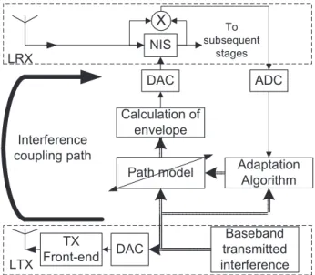
In the multimode transceiver the baseband transmitted interference is available locally. As shown in Fig. 1.9, using a discrete-time baseband model of the in-terference coupling path, shown with the tick line, the envelope of the receiver interference can be obtained digitally. The coupling path is subject to environ-mental changes. Hence the model must be adapted during the receiver operation to track these changes. The residual interference at the NIS output is measured
using a mixer with the NIS input as its local oscillator port. A closed-loop adapta-tion method is designed that adapts the model such that the power of the residual interference is minimized.
3DWKPRGHO
%DVHEDQG WUDQVPLWWHG LQWHUIHUHQFH 7;
)URQWHQG
1,6 '$&
/7; /5;
'$& ,QWHUIHUHQFH
FRXSOLQJSDWK
&DOFXODWLRQRI HQYHORSH
$GDSWDWLRQ $OJRULWKP
;
7RVXEVHTXHQW VWDJHV
$'&
Figure 1.9: NIS and its adaptation in the multimode transceiver.
1.4.2
Digital compensation of CM distortion
In practice an analogue circuit can only approximate an ideal characteristic. For example the ideal NIS as shown in Fig. 1.8) has a linear characteristic for the weak desired signal. Another example is a typical receiver front-end. Although it is desired to be linear, it shows nonlinear effects. When the combination of the strong interference and the weak desired signal passes through a block with a nonlinear characteristic, amplitude modulation of the interference is transferred to modulation of the desired signal, resulting in CM distortion. In this thesis, in two chapters the CM distortion is encountered, firstly, in a typical receiver without the NIS (Chapter 2), and secondly, in the receiver with a practical NIS circuit(Chapter 5). The CM distortion in these two cases can be avoided by increasing the linearity and perfecting the NIS circuit, respectively. Alternatively, the CM distortion can be digitally compensated by identifying a model of the nonlinearity and estimating the envelope of the interference at the input of the nonlinearity. Considering the continuous increase of digital computation power governed by Moore’s law, shifting the complexity from the analogue to the digital domain is advantageous in terms of circuit complexity and power consumption.
1.4 Proposed hybrid approach 13
In Chapter 2, we study the case that the interference is strong enough to cause CM distortion, although it is not so strong that it leads to desensitization. In this case a weakly nonlinear model, i.e. a third-order polynomial, can be used for the receiver front-end. A method is proposed to compensate the CM distortion by estimating the envelope of the received interference and the parameter of the model. In Chapter 5, the CM distortion is the result of the strong nonlinear effect of the NIS circuit. For this type of nonlinearity, an efficient way to model the dependency of the envelope and phase of the desired signal to envelope of the interference is to use a look-up table. The look-up table is measured during a calibration stage. Since the envelope of the interference is already estimated to adapt the NIS, by using the look-up table the CM distortion is compensated.
1.4.3
Other areas of application for the NIS
Similar to multimode operation, there are other applications where a strong local interference disrupts operation of a local receiver.
• Frequency Division Duplex (FDD) transceivers: In FDD transceivers the local transmitter of a given communication standard induces an interference on the local receiver of the same standard. Typically a duplexer filter is used to isolate the local transmitter from the local receiver. The duplexer filter is realized using surface acoustic wave or ceramic technology as external components. These are expensive and have fixed frequencies. Hence if a transceiver is meant to operate in several frequency bands a bank of duplexers should be used. Alternatively, a combination of a circulator and the NIS can be used to achieve isolation between the local transmitter and receiver.
• Frequency Modulated Continuous Wave (FMCW) radar: In FMCW radar the transmitted signal is also received by the radar receiver and can be many order of magnitudes stronger than the echoes received from targets.
• In basestations several transceivers of different standards are placed in close proximity. The limitations regarding the size and power consumption for the basestation, however, are much more relaxed compared to handheld devices.
• Radio Frequency Identification (RFID) readers: In RFID systems a transceiver, called reader, powers and communicates with tags that are within range. To maintain the flow of power from the reader to tags and enable communication with multiple tags the reader operates in full duplex. Owing to insufficient isolation between the transmitter and receiver of the reader, the transmitted signal induces interference in the receiver that is many orders of magnitude stronger than the signal reflected by the tags. Currently, to maintain the receiver sensitivity in the presence of such a strong interference, a receiver
with a large dynamic range and high power consumption is used.
1.5
Outline and contribution of this thesis
In this section we present a short summary of the content and contribution of each chapter of the rest of the thesis.
In Chapter 2, we analyze key distortion products which are generated in a receiver front-end having a memoryless nonlinear characteristic. When the combination of the strong interference and the weak desired signal experiences any nonlinear-ities in the receiver front-end, distortion products are generated. One of these is Cross-Modulation (CM) distortion, where the amplitude modulation of the inter-ference transfers to modulation of the desired signal. CM distortion is particularly problematic, since it occurs independent of the frequency separation of the desired signal and the interference. In this thesis we encounter CM distortion in two sit-uations, namely without and with NIS. The first situation is of interest since the interference can be weak enough to be handled without NIS yet strong enough to cause CM distortion. In this situation the CM distortion can be compensated digitally. In Chapter 2, we propose a fully digital compensation method that ex-ploits the local availability of the baseband interference to avoid the complexity and power dissipation of additional analogue circuits. The baseband interference is used as the reference for estimation and then compensation of the CM distortion. Although the proposed method in Chapter 2 is able to mitigate the CM distortion to some extent, it cannot alleviate the desensitization. In Chapter 3, we propose to use an adaptive Nonlinear Interference Suppressor (NIS), with the aim to prevent desensitization by suppressing the interference at an early stage of the receiver front-end. In previous work the NIS was only used for constant-envelope inter-ference. For interference with arbitrary envelope variations, firstly, we derive an optimal adaptation signal for the NIS that yields complete suppression of the in-terference in the absence of the desired signal. For this optimal adaptation signal, residual distortion products of the NIS are identified which are not present in the case of a constant-envelope interference. The impact of these products on the re-ceived desired signal is analyzed and rules of thumb are given to specify conditions for which adequate interference suppression is combined with negligible distortion. We show that these conditions are met in most cases of practical interest. The optimal adaptation signal is proportional to the envelope of the received interference at the NIS input. A key feature in the multimode transceiver is the local availability of the interference source. Using a baseband linear model of the interference coupling path, from the local transmitter to the local receiver, the adaptation signal can be obtained digitally. In Chapter 4, we quantify the
1.6 Publications 15
required accuracy for the adaptation signal to properly suppress the interference while keeping the degradation of the receiver Symbol Error Rate (SER) negligible. To provide the required accuracy, we propose a closed-loop method to dynamically adapt the path model such that the power of the residual interference at the output of the NIS is minimized. This method uses the baseband interference as a reference in order to combine simplicity with high accuracy and high speed. Our analysis and simulations show that the optimal adaptation signal can be estimated with sufficient accuracy, such that the interference is strongly suppressed while a SER close to that of an exactly linear receiver is achieved.
In Chapters 3 and 4, idealized models of the NIS and adaptation circuits are used to analyze the performance afforded by the NIS. In Chapter 5, we present experimental results of a multimode transceiver test bed that uses the mixed-signal integrated NIS circuit designed in [17]. The main circuit imperfections that limit the NIS performance are identified. Simple imperfection models are described that explain the experimental results. Based on these models, the NIS adaptation method is extended with simple digital compensation and calibration techniques that unlock the full interference suppression potential of the NIS circuit. Furthermore, a low-complexity digital compensation method is proposed for the CM distortion that is caused by the imperfections. Successful operation of the test bed suggests that the NIS approach is practical and attractive for multimode transceivers.
Concluding remarks and suggestions for future work are collected in Chapter 6. The analysis, simulation and experimental results in this thesis show that the NIS can achieve substantial interference suppression at attractive complexity and power dissipation, and that the residual distortion products can be digitally compensated with a low complexity. Both fundamental and practical limitations of the proposed approach are identified, and directions for future improvements are sketched.
1.6
Publications
The research work of this thesis resulted in the following publications.
1.6.1
Journal publications
H. Habibi, E.J.G. Janssen, Wu Yan, D. Milosevic, P.G.M. Baltus, J.W.M. Bergmans, ”Experimental evaluation of an Adaptive Nonlinear Interference Suppressor for Multimode Transceivers”, To be published in IEEE Journal on Emerging and Selected Topics in Circuits and Systems, Dec. 2013.
H. Habibi, E.J.G. Janssen, Wu Yan, P.G.M. Baltus, J.W.M. Bergmans, ”Closed-loop Adaptation of a Nonlinear Interference Suppressor for multimode Transceivers”, Submitted toIEEE Transaction on Vehicular Technology.
H. Habibi, E.J.G. Janssen, Wu Yan, P.G.M. Baltus, J.W.M. Bergmans, ”Sys-tem Study on Nonlinear Suppression of Varying-Envelope Local Interference in Multimode Transceivers”, Submitted to International Journal of Electronics and Communications.
H. Habibi, E.J.G. Janssen, Wu Yan, J.W.M. Bergmans, ”Digital Compensation of Cross-Modulation Distortion in Multimode Transceivers”IET communication, pp. 1724-1733, Aug. 2012.
1.6.2
Conference proceedings
H. Habibi, P.E. Ling, E.J.G. Janssen, Wu Yan, J.W.M. Bergmans, P.G.M. Bal-tus, ”Adaptive nonlinear interference suppressor for cognitive radio applications”,
Proceedings of Workshop on Cognitive Radio, Kista, Sweden, June, 2013.
H. Habibi, E.J.G. Janssen, Wu Yan, D. Milosevic, J.W.M. Bergmans, P.G.M. Baltus, ”Suppression of Constant Modulus Interference in Multimode Transceivers Using an Adaptive Nonlinear Circuit”. Proceedings of NASA/ESA Conference on Adaptive Hardware and Systems (AHS-2013), Turin, Italy June, 2013.
H. Habibi, E.J.G. Janssen, Wu Yan, P.G.M. Baltus, J.W.M. Bergmans, ”Non-linear Interference Suppressor for Varying-Envelope Local Interference in multi-mode transceivers”. Proceedings of 34th Symposium on Information Theory in the Benelux, Leuven, Belgium, May, 2013.
H. Habibi, E.J.G. Janssen, Wu Yan, P.G.M. Baltus, J.W.M. Bergmans, ”Closed-loop Adaptation of a Nonlinear Interference Suppressor for Local Interference in Multimode Transceivers”. Proceedings of 34th Symposium on Information Theory in the Benelux, Leuven, Belgium, May, 2013.
H. Habibi, E.J.G. Janssen, Wu Yan, J.W.M. Bergmans, P.G.M. Baltus, ”Suppres-sion of constant modulus interference in multimode transceivers by closed-loop tuning of a nonlinear circuit”. Proceedings of IEEE 75th Vehicular Technology Conference, Yokohama, Japan, May, 2012.
H. Habibi, E.J.G. Janssen, Wu Yan, J.W.M. Bergmans, ”Digital Compensation of Cross-Modulation Distortion in Multimode Transceivers”. Proceedings of IEEE 75th Vehicular Technology Conference, Yokohama, Japan, May, 2012.
1.6 Publications 17
E.J.G. Janssen, H. Habibi, D. Milosevic, P.G.M. Baltus and A.H.M van Roermund, ”Smart Self-Interference Suppression by Exploiting a Nonlinearity,” Invited paper in 22nd Workshop on Advances in Analog Circuit Design (AACD), Grenoble, France, April, 2013.
E.J.G. Janssen, H. Habibi, D. Milosevic, P.G.M. Baltus, A.H.M. van Roermund, ”Frequency-independent smart interference suppression for multi-standard transceivers”, Proceedings of the 42st European Microwave Conference (EuMC), Amsterdam, The Netherlands, November, 2012.
E.J.G. Janssen, H. Habibi, D. Milosevic, P.G.M. Baltus, A.H.M. van Roermund, ”Digital hardware resources for steering a nonlinear interference suppressor”. Pro-ceedings of the 19th International Conference Mixed Design of Integrated Circuits and Systems (MIXDES), Warsaw, Poland, May 2012.
E.J.G. Janssen, H. Habibi, D. Milosevic, P.G.M. Baltus, ”Modeling and Analysis of Nonlinearities and Bandwidth Limitations in RF Receivers”. Proceeding of IEEE International Symposium on Circuits and Systems (ISCAS), Rio de Janeiro, Brazil, May, 2011.
Appendix I:Single-branch analogue cancellation
In this appendix firstly we present the frequency response of the interference cou-pling path from the LTX to the LRX. Secondly, we analyze the performance of analogue cancelation using a single-branch model of the path. The simple in-vestigation performed in this appendix, clarifies the limitations of the analogue cancellation.
System setup
A simplified diagram of the multimode transceiver including a LTX and a LRX is shown in Fig. 1.10. we have two objectives to study the frequency response Hs(f) =Vr(f)
Vt(f) of the antenna coupling system. Firstly,|Hs(f)|
2 shows the power of the interference that is coupled from the LTX to the LRX. Secondly, we use this frequency response to study the performance of the analogue cancellation ap-proach, which was described in Section 1.3.3. In this appendix, we consider the simple system of Fig. 1.10 with simple antennas for the LTX and the LRX. Absence of highly frequency-selective components in Fig. 1.10 leads to favorable results for analogue cancellation approach compared to a practical multimode transceiver, where the antennas are designed to achieve more frequency selectivity and a filter is used after the LRX antenna. The performance of the cancellation attained in this appendix, however, can be considered as an upper bound on the performance of the cancellation approach. For the LTX and the LRX we consider frequency
t V
/7; /5;
r V
Figure 1.10: A simplified block diagram of LTX and LRX.
bands of 1.9 to 2 GHz and 2.4 to 2.5 GHz, respectively. Planar dipole antennas are used for both the LTX and the LRX. The distance d between the antennas is assumed to be 3, 5, or 10 cm. Scattering parametersS11 of both antennas are shown in Fig. 1.11 ford= 5 cm. The LTX and LRX antenna are tuned to have minimum reflections at 1.95 GHz and 2.45 GHz, repectively. Ford= 5 cm, how-ever, a slight deviation inS11 is observed, owing to the mutual coupling between the antennas. For d = 3 ,5 ,10 cm, the S-parameters of the antenna system is calculated using CST simulation software. Using the S-parameters,Hs(f) =Vr(f)
1.6 Appendix I:Single-branch analogue cancellation 19
1.8 1.9 2 2.1 2.2 2.3 2.4 2.5 2.6
−25 −20 −15 −10 −5 0
Frequency, GHz
2
0
lo
g1
0
(
|
S1
1
|
)
LTX antenna LRX antenna
Figure 1.11: Scattering parametersS11of LTX and LRX antenna.
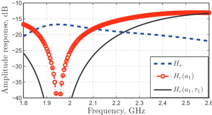
can be calculated1. The amplitude response 10 log
10(|Hs|2), shown in Fig. 1.12, indicates the amount of power that is transferred from the LTX to the LRX versus frequency. In two frequency ranges|Hs|is of interest.
1-In the band from 1.9 to 2 GHz: it indicates the amount of out-of-band interfer-ence received by the LRX from the LTX. For example if the LTX transmits at 30 dBm, then at the LRX an interference of about 13 dBm is received, ford= 5 cm. Such a strong interference can lead to desensitization of the receiver front-end if it is not suppressed sufficiently.
2-In the band from 2.4 to 2.5 Ghz: it indicates the amount of in-band interference. The amplified thermal noise accompanied by the LTX can be 50 dB stronger than the thermal noise floor. A 20 dB coupling loss between LTX and LRX in this band, as seen in Fig. 1.12, leads to an in-band noise which can be 30 dB stronger than the LRX input thermal noise. Hence the transmitted noise by the LTX can significantly disrupt the LRX.
At a first sight, the analogue interference cancellation seems to provide a solution for both out-of-band interference and in-band noise. This would be possible if an analogue model of Hs could be constructed with enough accuracy over both frequency bands of the LTX transmission and the LRX reception. In principle an analogue model with several branches, as shown in Fig. 1.13, can be used to con-structHs(f). As discussed in Section 1.3.3, owing to complexity of a multi-branch analogue model, most works in the state of the art consider a single-branch variant of the model in Fig. 1.13, without any delay element. In the following sections, we analyze the performance of the single-branch model with and without a delay element.
1.8 1.9 2 2.1 2.2 2.3 2.4 2.5 2.6 −40
−35 −30 −25 −20 −15 −10
Frequency, GHz
1
0
∗
lo
g1
0
(
|
H
s
|
2 )
d=3 cm d=5 cm d=10 cm
Figure 1.12: Frequency response of the system for different spacing between an-tennas.
*DLQ 'HOD\
τ
D
*DLQ 'HOD\ Q
τ
QD
#
$QDORJXHPRGHO W
9 I
9 I
U9
FI
Figure 1.13: Interference cancellation using an analogue model ofHs(f).
Single-branch model without delay
A single-branch variant of Fig. 1.13, without a delay element is shown in Fig. 1.14. To make the cancellation possible,a1must be complex-valued. A complex-valued scaling can be implemented by combining a variable gain amplifier and a vector modulator. By adapting a1 the frequency response of the cancellation system Hc(f, a1) = Vc(f)
Vt(f) can be nulled at a single frequency. Fig. 1.15 showsHc(f, a1) and compares it withHs(f), whena1 is tuned to obtain a null at 1.95 GHz. We see that a narrowband null is attained at 1.95 GHz at the expense of an increased coupling of the LTX noise at the frequency range of 2.4-2.5 GHz. To measure effectiveness of the cancellation system we define Interference Cancellation (IC)
1.6 Appendix I:Single-branch analogue cancellation 21
*DLQ
D
W
9 I 9 IU 9F I
Figure 1.14: Cancellation using a single-branch without delay.
1.8 1.9 2 2.1 2.2 2.3 2.4 2.5 2.6
−40 −35 −30 −25 −20 −15 −10
Frequency, GHz
Am
p
li
tu
d
e
re
sp
o
n
se
,
d
B
Hs Hc(a1)
Figure 1.15: Frequency response of the system before and after cancellation.
for a center frequency fi and bandwidthBi of the interference as:
IC =
∫fi+Bi2
fi−Bi2
|Hs(f)|2
∫fi+Bi2
fi−Bi2 |
Hc(f)|2
. (1.1)
For an interference with a flat spectrum over [fi−Bi
2, fi+ Bi
2], IC indicates the ratio of the interference power before cancellation to the interference power after cancellation. For fi in range of 1.9 to 2 GHz, IC is maximized by adapting a1. The maximum of IC versusfi forBi=20 MHz is shown in Fig. 1.16. We see that an IC of about 25-27 dB can be attained.
Single-branch model with adaptable complex-valued gain and
adaptable delay
The group delay of the system in Fig. 1.10 is shown in Fig. 1.17. We see a group delay in the order of 1 ns, which the model without the delay cannot handle. To improve the performance of the cancellation, in this section we consider a single-branch model with adaptablea1andτ1. Fig. 1.18 showsHc(f, a1, τ1) whena1and τ1are tuned to obtain a null at 1.95 GHz. For comparisonHs(f) andHc(f, a1) are
1.9 1.92 1.94 1.96 1.98 2 20
25 30 35 40
fi, GHz
IC
,
d
B
d=3 cm d=5 cm d=10 cm
Figure 1.16: Interference cancellation with a single complex-valued gain, Bi =20 MHz andd=5 cm.
1.8 1.9 2 2.1 2.2 2.3 2.4 2.5 2.6
0.4 0.5 0.6 0.7 0.8 0.9 1 1.1
Frequency, GHz
G
ro
u
p
d
el
a
y,
n
s
d=3 cm d=5 cm d=10 cm
Figure 1.17: Group delay of the system in Fig. 1.10.
also shown. We see that although the null forHc(f, a1, τ1) is widened compared toHc(f, a1), the coupling across the band from 2.4 to 2.5 GHz is still increased by about 10 dB. Forfi in the range of 1.9 to 2 GHz, IC is maximized by adaptinga1 andτ1. The maximum of IC versusfi forBi=20 MHz is shown in Fig. 1.19. We see that an IC of better than 40 dB can be attained.
1.6 Appendix I:Single-branch analogue cancellation 23
1.8 1.9 2 2.1 2.2 2.3 2.4 2.5 2.6
−40 −35 −30 −25 −20 −15 −10
Frequency, GHz
Am
p
li
tu
d
e
re
sp
o
n
se
,
d
B
Hs Hc(a1) Hc(a1, τ1)
Figure 1.18: Amplitude response before and after cancellation with adaptable gain and delay.
1.9 1.92 1.94 1.96 1.98 2
20 30 40 50 60 70
fi, GHz
IC
,
d
B
d=3 cm d=5 cm d=10 cm
Figure 1.19: Interference cancellation with an adaptable gain and delay, Bi =20 MHz andd=5 cm.
Chapter 2
Digital Compensation of
Cross-Modulation Distortion
in Multimode Transceivers
1
2.1
Abstract
In a multimode transceiver, several communication standards may be active at the same time. Due to the small size of the transceiver, the transmitter for one standard induces a large interference on the receiver for another one. When this large interference passes through the inherently nonlinear receiver Front-End (FE), distortion products are generated. Among these products, the Cross-Modulation (CM) product is the most problematic one, as it always has the same center fre-quency as the desired signal. Increasing the FE linearity to lower the CM distortion leads to unacceptable power consumption for a handheld device. Considering the continuous increase of digital computation power governed by Moore’s law an at-tractive alternative approach is to digitally compensate for the CM distortion. An existing solution to compensate for the CM distortion is tailored to single-mode transceivers and requires an auxiliary FE. By using the locally available trans-mitted interference in the multimode transceiver, we propose a CM compensation method which requires no additional analog hardware. Hence the power consump-tion and complexity of the multimode transceiver can be reduced significantly. The simulation results demonstrate that the proposed method can lower distortion to 1This chapter is reproduced from the paper published as H. Habibi, E.J.G. Janssen, Wu Yan, J.W.M. Bergmans, ”Digital Compensation of Cross-Modulation Distortion in Multimode Transceivers”,IET communication, pp. 1724-1733, Aug. 2012.
a negligible amount at realistic interference levels.
2.2
Introduction
The communication features of handheld devices have been increasing rapidly in the past years. Some of the possible communication standards that may be supported by a handheld device are GSM, CDMA, WLAN, WiMAX, Bluetooth, and GPS. To implement these standards, a combinations of several transceivers is required which is called a multimode transceiver [18]. In a multimode transceiver, several standards may be active at the same time.
:L0$; /7; :/$1
57;
:/$1 /5; 0XOWLPRGH WUDQVFHLYHU 5
G
W
5
L
W
&RXSOLQJ
5
[
W
Figure 2.1: A sample scenario in a multi-mode transceiver.
Fig. 2.1 shows a sample scenario which includes a Remote WLAN Transmitter (RTX), a Local WLAN receiver (LRX), and a Local WiMAX Transmitter (LTX). The RTX transmits a WLAN signal with a carrier frequency fd in the range of 2400-2483 MHz. This signal passes through a communication channel and is received by the LRX antenna as the received desired signal dR(t). At the same time the LTX transmits a WiMAX signal with a carrier frequencyfi in the range of 2496-2690 MHz, which is partly received by the LRX antenna after a coupling loss and induces an interferer iR(t). The coupling loss between transceivers in a multimode transceiver is typically between 10 to 30 dB [19]. The LTX output power can be as high as 23 dBm while the LRX sensitivity can be as low as -83 dBm [20]. Hence the received signal xR(t) includes both dR(t) and iR(t) where the power ofiR(t) can be 96 dB larger than that ofdR(t). The high level ofiR(t) compared to that ofdR(t) is one of the main challenges in the implementation of a multimode transceiver.
The direct conversion receiver architecture is a popular choice for implementation in integrated circuits. Fig. 2.2 shows such a receiver tuned to a center frequency fd. The received signal xR(t) is passed through a Band Pass filter (BPF) which limits the input frequency range to frequency band of the standard. The BPF suppressesiR(t) to some extent. However the BPF suppression is limited to about 0-40 dB depending on the frequency separation between iR(t) and dR(t) (0 dB for standards that share the same frequency band). Hence the BPF outputxB(t)

![Figure 2.6: MSE {ˆτ i } versus SDR{z} for N = 10 3 , 10 4 , d[p d ]: QPSK, 64 QAM and OFDM.](https://thumb-us.123doks.com/thumbv2/123dok_us/8534295.2296975/55.722.149.543.211.510/figure-mse-ˆτ-versus-sdr-qpsk-qam-ofdm.webp)
![Figure 2.7: MSE{ˆc}versus SDR, N = 10 3 , 10 4 , d[p d ]: OFDM..](https://thumb-us.123doks.com/thumbv2/123dok_us/8534295.2296975/56.722.176.550.476.792/figure-mse-ˆc-versus-sdr-n-d-ofdm.webp)
![Figure 2.8: MSE{ˆc}versus SDR, N = 10 4 , d[p d ]: QPSK, 64 QAM and OFDM..](https://thumb-us.123doks.com/thumbv2/123dok_us/8534295.2296975/57.722.151.536.149.460/figure-mse-ˆc-versus-sdr-qpsk-qam-ofdm.webp)
![Fig. 2.8 shows MSE{ˆc} for various modulations of d[p d ] where N = 10 4 indepen- indepen-dent samples of i[p i ] and d[p d ] are used to estimate c.](https://thumb-us.123doks.com/thumbv2/123dok_us/8534295.2296975/58.722.197.535.341.608/fig-shows-various-modulations-indepen-indepen-samples-estimate.webp)
![Figure 2.10: SER versus SDR{z}, N = 10 4 , a) d[p d ]: QPSK, 64 QAM and OFDM, b)d[p d ] : 64 QAM](https://thumb-us.123doks.com/thumbv2/123dok_us/8534295.2296975/59.722.177.519.147.428/figure-ser-versus-sdr-qpsk-qam-ofdm-qam.webp)
