Quasi-Resonant Primary
Side Current-Mode
Controller for LED Lighting
Below 25 W
NCL37733
The NCL37733 is a compact driver for power−factor corrected flyback and non−isolated buck−boost and SEPIC converters. The controller operates in a quasi−resonant mode to provide optimal efficiency, and embeds a proprietary control method which allows the LED current to be tightly regulated from the primary side, thus eliminating the need for a secondary−side feedback circuitry and for an optocoupler.
Housed in a TSOP−6 package, the device is highly integrated with a minimum number of external components. A robust suite of safety protection is built in to simplify the design. This device is specifically intended for very compact space efficient designs.
Features
•
Quasi−resonant Peak Current−mode Control Operation•
Constant Current Control with Primary Side Feedback•
Tight LED Constant Current Regulation of ±2% typical•
Near−Unity Power Factor (>0.95 typically)•
Optimized for Line Wide−range Applications•
Line Feedforward for Enhanced Regulation Accuracy•
Low Start−up Current (10 mA typ.)•
Wide VCC Range•
100 mA / 150 mA Totem Pole Driver with 12 V Gate Clamp•
Robust Protection Features♦ OVP on VCC
♦ Programmable Over Voltage / LED Open Circuit Protection
♦ Cycle by cycle peak current limit
♦ Winding Short Circuit Protection ♦ Secondary Diode Short Protection ♦ Output Short Circuit Protection ♦ Thermal Shutdown
♦ VCC Undervoltage Lockout ♦ Brown−Out Detection
•
Pb−Free, Halide−Free MSL1 Product Typical Application•
Integral LED Bulbs and Tubes below 25 W•
LED Drivers / Power Supplies below 25 Wwww.onsemi.com
ORDERING INFORMATION
Device Package Shipping†
NCL37733BSNT1G TSOP−6
(Pb−Free/ Halide Free)
3000 / Tape & Reel TSOP−6
CASE 318G−02
MARKING DIAGRAM
†For information on tape and reel specifications, including part orientation and tape sizes, please refer to our Tape and Reel Packaging Specification Brochure, BRD8011/D.
(Note: Microdot may be in either location)
PIN CONNECTIONS
1 2 3
6 5 4 CS/ZCD
GND COMP
DRV VCC
VS
1
2T4 = Specific Device Code A =Assembly Location
Y = Year
W = Work Week
G = Pb−Free Package 2T4AYWG
G 1
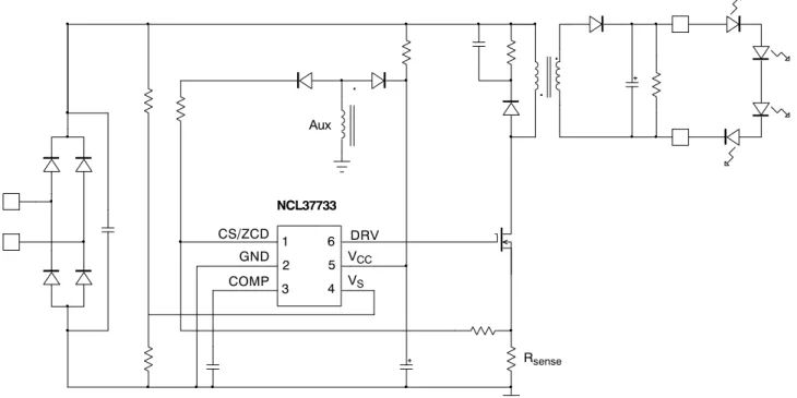
TYPICAL APPLICATION SCHEMATIC
Figure 1. Typical Application Schematic in a Flyback Converter
. .
Aux
.
NCL37733 1 2 3
6 5 4
DRV GND
CS/ZCD COMP
VCC
VS
Rsense
Figure 2. Typical Application Schematic in a Buck−Boost Converter
. .
Aux
NCL37733 1 2 3
6 5 4
DRV GND
CS/ZCD COMP
VCC
VS
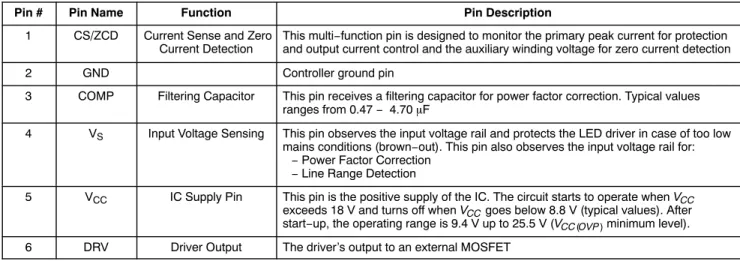
Table 1. PIN FUNCTION DESCRIPTION
Pin # Pin Name Function Pin Description
1 CS/ZCD Current Sense and Zero
Current Detection This multi and output current control and the auxiliary winding voltage for zero current detection−function pin is designed to monitor the primary peak current for protection
2 GND Controller ground pin
3 COMP Filtering Capacitor This pin receives a filtering capacitor for power factor correction. Typical values ranges from 0.47 − 4.70 mF
4 VS Input Voltage Sensing This pin observes the input voltage rail and protects the LED driver in case of too low
mains conditions (brown−out). This pin also observes the input voltage rail for:
− Power Factor Correction
− Line Range Detection
5 VCC IC Supply Pin This pin is the positive supply of the IC. The circuit starts to operate when VCC exceeds 18 V and turns off when VCC goes below 8.8 V (typical values). After start−up, the operating range is 9.4 V up to 25.5 V (VCC(OVP) minimum level).
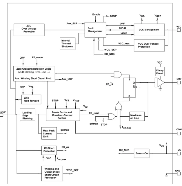
INTERNAL CIRCUIT ARCHITECTURE
Figure 3. Internal Circuit Architecture ZCD
Over Voltage Protection
Zero Crossing Detection Logic (ZCD Blanking, Time−Out, ...)
CS/ZCD Power Factor and Constant−Current
Control Leading
Edge Blanking
Winding and Output Diode Short Circuit Protection Max. Peak Current Limit
Ipkmax
WOD_SCP DRV
VCC Management
VCC
DRV VCC Over Voltage
Protection
VCC Internal
Thermal Shutdown
Fault Management
Clamp Circuit
VS Brown−Out
BO_NOK S
R Q Q
CS_reset
STOP
UVLO OFF
Latch
STOP WOD_SCP BO_NOK
GND STOP
Aux. Winding Short Circuit Prot. Aux_SCP Aux_SCP
VCC_max
V Line
feed−forward
VS VVS
Ipkmax
VREF VDD
Enable
CS Short Protection
CS_ok
CS_ok FF_mode
Maximum on time
UVLO ton,max
on,max t VVS
COMP VREF
TF V DRV
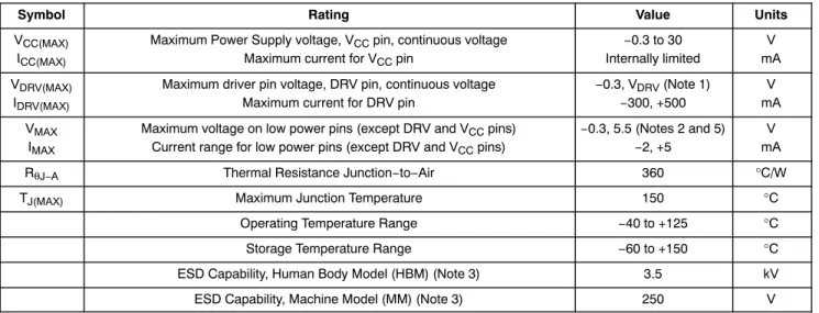
Table 2. MAXIMUM RATINGS TABLE
Symbol Rating Value Units
VCC(MAX)
ICC(MAX)
Maximum Power Supply voltage, VCC pin, continuous voltage
Maximum current for VCC pin
−0.3 to 30 Internally limited
V mA VDRV(MAX)
IDRV(MAX)
Maximum driver pin voltage, DRV pin, continuous voltage Maximum current for DRV pin
−0.3, VDRV (Note 1) −300, +500
V mA VMAX
IMAX
Maximum voltage on low power pins (except DRV and VCC pins)
Current range for low power pins (except DRV and VCC pins)
−0.3, 5.5 (Notes 2 and 5)
−2, +5
V mA
RθJ−A Thermal Resistance Junction−to−Air 360 °C/W
TJ(MAX) Maximum Junction Temperature 150 °C
Operating Temperature Range −40 to +125 °C
Storage Temperature Range −60 to +150 °C
ESD Capability, Human Body Model (HBM) (Note 3) 3.5 kV
ESD Capability, Machine Model (MM) (Note 3) 250 V
Stresses exceeding those listed in the Maximum Ratings table may damage the device. If any of these limits are exceeded, device functionality should not be assumed, damage may occur and reliability may be affected.
1. VDRV is the DRV clamp voltage VDRV(high) when VCC is higher than VDRV(high). VDRV is VCC otherwise.
2. This level is low enough to guarantee not to exceed the internal ESD diode and 5.5 V ZENER diode. More positive and negative voltages can be applied if the pin current stays within the −2 mA / 5 mA range.
3. This device contains ESD protection and exceeds the following tests: Human Body Model 3500 V per JEDEC Standard JESD22−A114E, Machine Model Method 250 V per JEDEC Standard JESD22−A115B.
4. This device contains latch−up protection and exceeds 100 mA per JEDEC Standard JESD78. 5. Recommended maximum VS voltage for optimal operation is 4 V.
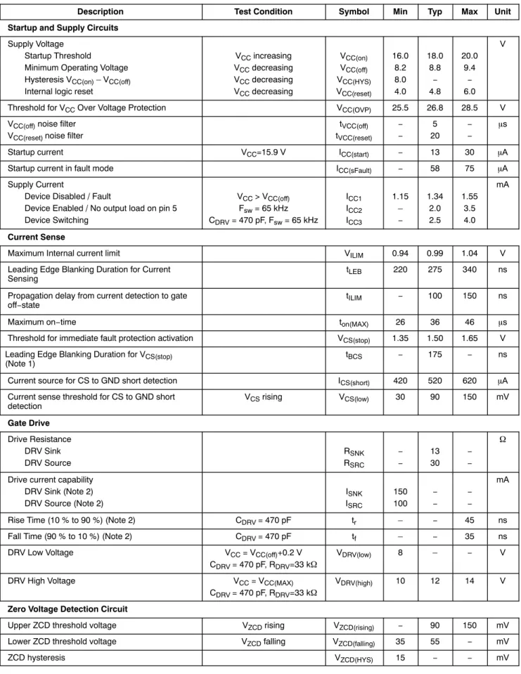
Table 3. ELECTRICAL CHARACTERISTICS
(Unless otherwise noted: For typical values TJ = 25°C, VCC = 12 V, VCS/ZCD = 0 V
For min/max values TJ = −40°C to +125°C, Max TJ = 150°C, VCC = 12 V)
Description Test Condition Symbol Min Typ Max Unit
Startup and Supply Circuits Supply Voltage
Startup Threshold
Minimum Operating Voltage Hysteresis VCC(on) – VCC(off)
Internal logic reset
VCC increasing
VCC decreasing
VCC decreasing
VCC decreasing
VCC(on) VCC(off) VCC(HYS) VCC(reset) 16.0 8.2 8.0 4.0 18.0 8.8 − 4.8 20.0 9.4 − 6.0 V
Threshold for VCC Over Voltage Protection VCC(OVP) 25.5 26.8 28.5 V
VCC(off) noise filter
VCC(reset) noise filter
tVCC(off) tVCC(reset) − − 5 20 − − m s
Startup current VCC=15.9 V ICC(start) − 13 30 mA
Startup current in fault mode ICC(sFault) − 58 75 mA
Supply Current
Device Disabled / Fault
Device Enabled / No output load on pin 5 Device Switching
VCC > VCC(off)
Fsw = 65 kHz
CDRV = 470 pF, Fsw = 65 kHz
ICC1 ICC2 ICC3 1.15 – − 1.34 2.0 2.5 1.55 3.5 4.0 mA Current Sense
Maximum Internal current limit VILIM 0.94 0.99 1.04 V
Leading Edge Blanking Duration for Current
Sensing tLEB 220 275 340 ns
Propagation delay from current detection to gate
off−state tILIM − 100 150 ns
Maximum on−time ton(MAX) 26 36 46 ms
Threshold for immediate fault protection activation VCS(stop) 1.35 1.50 1.65 V
Leading Edge Blanking Duration for VCS(stop)
(Note 1) tBCS − 175 − ns
Current source for CS to GND short detection ICS(short) 420 520 620 mA
Current sense threshold for CS to GND short
detection VCS rising VCS(low) 30 90 150 mV
Gate Drive Drive Resistance DRV Sink DRV Source RSNK RSRC − − 13 30 − − W
Drive current capability DRV Sink (Note 2) DRV Source (Note 2)
ISNK ISRC 150 100 − − − − mA
Rise Time (10 % to 90 %) (Note 2) CDRV = 470 pF tr – − 45 ns
Fall Time (90 % to 10 %) (Note 2) CDRV = 470 pF tf – − 35 ns
DRV Low Voltage VCC = VCC(off)+0.2 V
CDRV = 470 pF, RDRV=33 kW
VDRV(low) 8 – − V
DRV High Voltage VCC = VCC(MAX)
CDRV = 470 pF, RDRV=33 kW
VDRV(high) 10 12 14 V
Zero Voltage Detection Circuit
Upper ZCD threshold voltage VZCD rising VZCD(rising) − 90 150 mV
Lower ZCD threshold voltage VZCD falling VZCD(falling) 35 55 − mV
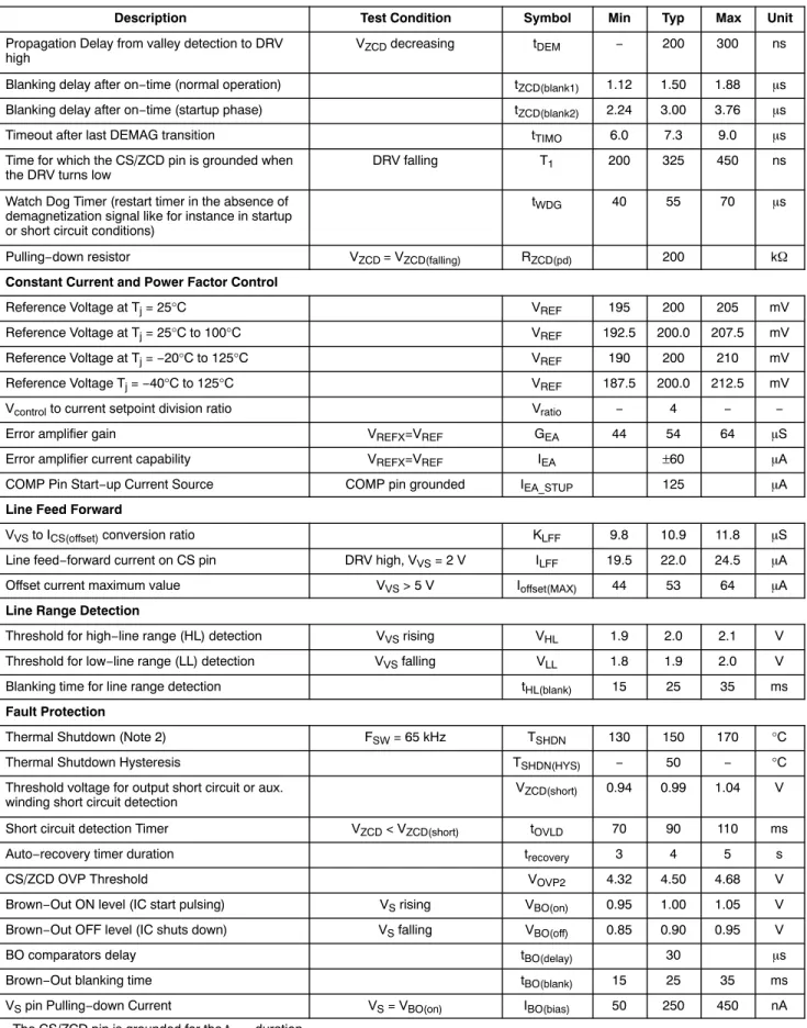
Table 3. ELECTRICAL CHARACTERISTICS
(Unless otherwise noted: For typical values TJ = 25°C, VCC = 12 V, VCS/ZCD = 0 V
For min/max values TJ = −40°C to +125°C, Max TJ = 150°C, VCC = 12 V)
Description Test Condition Symbol Min Typ Max Unit
Propagation Delay from valley detection to DRV
high VZCD decreasing tDEM − 200 300 ns
Blanking delay after on−time (normal operation) tZCD(blank1) 1.12 1.50 1.88 ms
Blanking delay after on−time (startup phase) tZCD(blank2) 2.24 3.00 3.76 ms
Timeout after last DEMAG transition tTIMO 6.0 7.3 9.0 ms
Time for which the CS/ZCD pin is grounded when
the DRV turns low DRV falling T1 200 325 450 ns
Watch Dog Timer (restart timer in the absence of demagnetization signal like for instance in startup or short circuit conditions)
tWDG 40 55 70 ms
Pulling−down resistor VZCD = VZCD(falling) RZCD(pd) 200 kW
Constant Current and Power Factor Control
Reference Voltage at Tj = 25°C VREF 195 200 205 mV
Reference Voltage at Tj = 25°C to 100°C VREF 192.5 200.0 207.5 mV
Reference Voltage at Tj = −20°C to 125°C VREF 190 200 210 mV
Reference Voltage Tj = −40°C to 125°C VREF 187.5 200.0 212.5 mV
Vcontrol to current setpoint division ratio Vratio − 4 − −
Error amplifier gain VREFX=VREF GEA 44 54 64 mS
Error amplifier current capability VREFX=VREF IEA ±60 mA
COMP Pin Start−up Current Source COMP pin grounded IEA_STUP 125 mA
Line Feed Forward
VVS to ICS(offset) conversion ratio KLFF 9.8 10.9 11.8 mS
Line feed−forward current on CS pin DRV high, VVS = 2 V ILFF 19.5 22.0 24.5 mA
Offset current maximum value VVS > 5 V Ioffset(MAX) 44 53 64 mA
Line Range Detection
Threshold for high−line range (HL) detection VVS rising VHL 1.9 2.0 2.1 V
Threshold for low−line range (LL) detection VVS falling VLL 1.8 1.9 2.0 V
Blanking time for line range detection tHL(blank) 15 25 35 ms
Fault Protection
Thermal Shutdown (Note 2) FSW = 65 kHz TSHDN 130 150 170 °C
Thermal Shutdown Hysteresis TSHDN(HYS) − 50 − °C
Threshold voltage for output short circuit or aux.
winding short circuit detection VZCD(short) 0.94 0.99 1.04 V
Short circuit detection Timer VZCD < VZCD(short) tOVLD 70 90 110 ms
Auto−recovery timer duration trecovery 3 4 5 s
CS/ZCD OVP Threshold VOVP2 4.32 4.50 4.68 V
Brown−Out ON level (IC start pulsing) VS rising VBO(on) 0.95 1.00 1.05 V
Brown−Out OFF level (IC shuts down) VS falling VBO(off) 0.85 0.90 0.95 V
BO comparators delay tBO(delay) 30 ms
APPLICATION INFORMATION The NCL37733 is designed to control flyback−,
buck−boost− and SEPIC−based LED drivers. A proprietary circuitry ensures accurate primary−side regulation of the output current (without the need for a secondary−side feedback) and near−unity power factor correction. The circuit contains a suite of powerful protections to ensure a robust LED driver design without the need for extra components or overdesign.
•
Quasi−Resonance Current−Mode Operation: implementing quasi−resonance operation in peak current−mode control, the NCL37733 optimizes the efficiency by switching in the valley of the MOSFET drain−source voltage in low−line conditions. When in high line, the circuit skips one valley to lower the switching frequency.•
Primary Side Constant Current Control with Power Factor Correction:proprietary circuitry allows the LED driver to achieve both near−unity power factor correction and accurate regulation of the output current without requiring any secondary−side feedback (no optocoupler needed). A power factor as high as 0.99 and an output current deviation below ±2% are typically obtained.
•
Main protection features:♦ Programmable Over−Voltage Protection (OVP2):
The CS/ZCD pin provides a programmable OVP protection. Adjust the external ZCD resistors divider or add a Zener diode to adjust the protection
threshold: if the CS/ZCD pin voltage exceeds 4.5 V (during the demagnetization time) for 4 consecutive
switching cycles, the controller stops operating for the 4−s auto−recovery delay.
♦ Cycle−by−cycle peak current limit:
when the current sense voltage exceeds the internal threshold VILIM, the MOSFET is immediately
turned off (cycle by cycle current limitation).
♦ Winding or Output Diode Short−Circuit Protection
(WODSCP):
an additional comparator senses the CS signal and stops the controller if it exceeds 150% x VILIM for 4
consecutive cycles. This feature can protect the converter if a winding is shorted or if the output diode is shorted or simply if the transformer saturates.
♦ Auxiliary Short−circuit protection (AUX_SCP):
If the ZCD pin voltage remains low for a 90 ms time interval, the controller detects that the output or the ZCD pin is grounded and hence, stops pulsating until a 4 s time has elapsed.
♦ Open LED protection:
if the LED string is open, the output voltage will rise and lead the programmable over−voltage protection (OVP2) or the VCC OVP to trip (VCC OVP trips
when the VCC pin voltage exceeds the VCC(OVP)
threshold – 26.8 V typically). In such a case, the controller shuts down and waits 4 seconds before restarting switching operation.
♦ Floating or Short Pin Detection:
the circuit can detect most of these situations which helps pass safety tests.
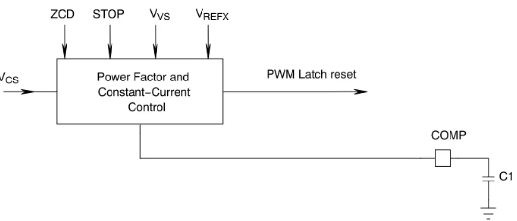
Constant Current Control
The NCL37733 embeds an analog/digital block to control the power factor and regulate the output current by monitoring the ZCD, VS and CS pin voltages (signals ZCD,
VS and VCS of Figure 4). This circuitry generates the current
setpoint (VCONTROL) and compares it to the current sense
signal (VCS) to dictate the MOSFET turning off event when
VCS exceeds VCONTROL.
Figure 4. Power Factor and Constant−Current Control
Power Factor and Constant−Current
Control
PWM Latch reset STOP
COMP ZCD
C1 VCS
VVS VREFX
As illustrated in Figure 4, the VS pin provides the
sinusoidal reference necessary for shaping the input current. The obtained current reference is further modulated so that when averaged over a half−line period, it is equal to the output current reference (VREFX). This averaging process is
made by an internal Operational Trans−conductance Amplifier (OTA) and the capacitor connected to the COMP pin (C1 of Figure 4). Typical COMP capacitance is 1 mF and should not be less than 470 nF to ensure stability. The COMP ripple does not affect the power factor performance as the circuit digitally eliminates it when generating the current setpoint.
If the VS pin properly conveys the sinusoidal shape, power
factor will be close to unity and the Total Harmonic Distortion (THD) will be low. In any case, the output current will be well regulated following the equation below:
Iout+ VREF
2 NPSRsense (eq. 1)
Where:
•
NPS is the secondary to primary transformer turnsNPS = NS / NP
•
Rsense is the current sense resistor (see Figure 1).•
VREF is the output current internal reference (200 mV).Whenever a major fault is detected which forces the auto−recovery mode, the COMP pin is grounded for the 4−s interruption. This is also the case if one of these situations is detected: brown−out, UVLO, TSD fault. This ensures a clean start−up when the circuit resumes operation.
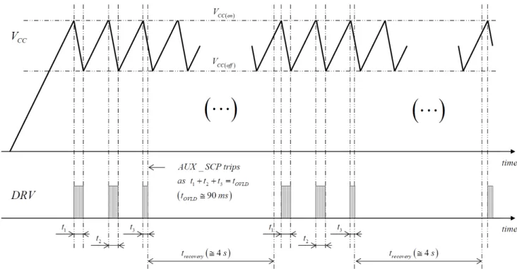
Start−up Sequence
Generally an LED lamp is expected to emit light in < 1 s and typically within 500 ms. The start−up phase consists of the time to charge the VCC capacitor, to begin switching and
the time to charge the output capacitor until sufficient current flows into the LED string. To speed−up this phase, the following characteristics define the start−up sequence:
•
The COMP pin is grounded when the circuit is off. The average COMP voltage needs to exceed the VS pinpeak value to have the LED current properly regulated (whatever the current target is). To speed−up the COMP capacitance charge and shorten the start−up phase, an internal 80 mA current source adds to the OTA sourced current (60 mA max typically) to charge up the COMP capacitance. The 80 mA current source remains on until the OTA starts to sink current as a result of the COMP pin voltage sufficient rise. At that moment, the COMP pin being near its steady−state value, only the OTA drives the COMP pin.
•
If the load is shorted, the circuit will operate in hiccup mode with VCC oscillating between VCC(off) andVCC(on) until the Auxiliary Short Circuit Protection,
AUX_SCP, forces the 4 s auto−recovery delay to reduce the operation duty−ratio (AUX_SCP trips if the ZCD pin voltage does not exceed 1 V within a 90 ms active period of time thus indicating a short to ground of the ZCD pin or an excessive load preventing the output voltage from rising). Figure 5 illustrates a start−up sequence with the output shorted to ground.
Figure 5. Start−up Sequence in a Load Short−circuit Situation Zero Crossing Detection Block
The CS/ZCD pin detects when the drain−source voltage of the power MOSFET reaches a valley by crossing down the 55 mV internal threshold and initiates a new DRV pulse at that moment. At startup and in overload conditions, the ZCD comparator may not be able to detect the demagnetization signal. To allow a new DRV pulse to occur, the NCL37733 features a watchdog timer which initiates a DRV pulse if the CS/ZCD pin voltage does not trig the ZCD comparator for the watchdog time. The watchdog duration is typically 55 ms at low line. It increases to 62 ms when the line range is detected (see next section).
As detailed in next section, the NCL37733 operates in QR mode at low line and at valley 2 in high−line conditions. If the auxiliary winding free oscillations are extremely damped, the ZCD comparator may not be able to detect the second valley as necessary at high line. To overcome this high−line situation, the NCL37733 features a time−out circuit to initiate a DRV pulse if once the demagnetization is detected, the CS/ZCD pin voltage stays below the ZCD comparator internal threshold for about 7.3 ms. Hence, the time−out acts as a substitute clock for valley−2 detection. In other words:
•
The timeout timer initiates a DRV pulse at high line if valley 1 is detected but valley 2 cannot be detected.•
The watchdog timer prevents the circuit from keeping permanently off if no demagnetization signal can be detected (e.g. at startup).Whenever the controller enters operation (cold startup, restart after a failure to startup at the first attempt or
operation recovery after a fault), the ZCD blanking time is tZCD(blank2) (3 ms typically) and keeps this value until the
ZCD signal is high enough to be detected by the ZCD comparator (higher than VZCD(rising), 90 mV typically). At
that moment, the ZCD blanking time recovers its nominal level (tZCD(blank1) =1.5 ms, typically).
If the ZCD pin or the auxiliary winding happen to be shorted, the watchdog function would normally make the controller keep switching and hence lead to improper LED current regulation. The “AUX_SCP” protection prevents such a stressful operation: a timer starts counting which is only reset when the ZCD voltage exceeds the VZCD(short)
threshold (1 V typically). If this timer reaches 90 ms (no ZCD voltage pulse having exceeded VZCD(short) for this time
period), the controller detects a fault and stops operation for 4 seconds.
The CS/ZCD pin is grounded for 325 ns (time T1 of the
parametric table) when the drive turns low. This prevents a possible CS residual voltage to be taken into account by the ZCD comparator, which could otherwise occur in particular if a filtering capacitor was added to the pin. Similarly, the CS/ZCD pin is “reset” when the drive turns high. Practically, the pin is grounded for the 175 ns tBCS time (Leading Edge
Blanking Duration for VCS(stop))to in this case, avoid that a
VAUX remaining voltage alters the current sense block operation.
For an optimal operation, the maximum ZCD level should be maintained below 5 V to stay safely below the built in clamping voltage of the pin.
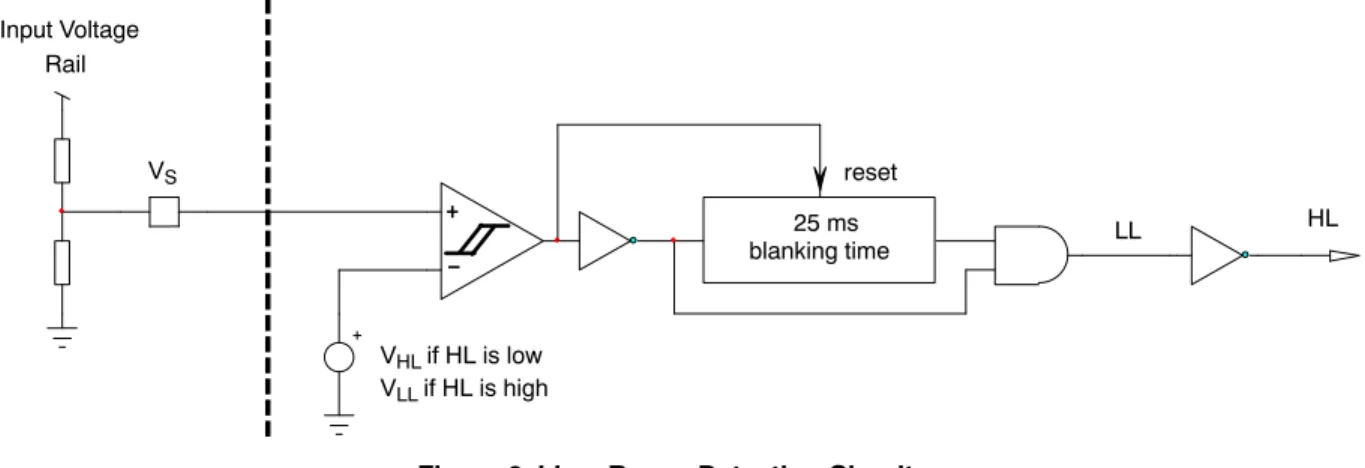
Line Range Detection
As sketched in Figure 6, this circuit detects the low−line range if the VS pin remains below the VLL threshold (1.9 V
typical) for more than the 25 ms blanking time. The high−line range is detected (“HL” of Figure 6 is high) as
soon as the VS pin voltage exceeds VHL (2.0 V typical).
These levels roughly correspond to 152 V rms and 160 V rms line voltages if the external resistors divider applied to the VS pin is designed to provide a 1 V peak value
at 80 V rms.
Figure 6. Line Range Detection Circuitry
25 ms blanking time
reset +
−
LL HL
Input Voltage Rail
VS
VHL if HL is low
VLL if HL is high
In the low−line range, conduction losses are generally dominant. Adding a dead−time would further increase these losses by forcing increased switching current. In high−line conditions, switching losses generally are the most critical. It is thus efficient to skip one valley to lower the switching frequency. Hence, under normal operation, the NCL37733
optimizes the efficiency over the line range by turning on the MOSFET at the first valley in low−line conditions and at the second valley in the high−line case. This is illustrated by Figure 7 that sketches the MOSFET Drain−source voltage in both cases.
Figure 7. Quasi−resonant Mode in Low Line (left), Turn on at Valley 2 when in High Line (right) In addition, the gain of the current control block is divided
by two when the high−line range is detected. This allows for an optimal resolution of the output current over the line range.
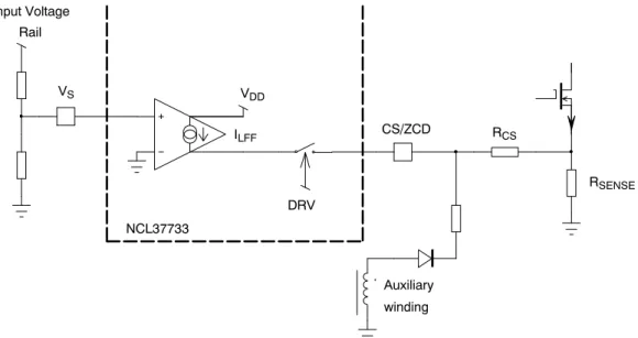
Line Feedforward
The NCL37733 computes the current setpoint (Vcontrol)
for power factor correction and proper regulation of the LED
current. Now, the MOSFET cannot turn off at the very moment when the current−sense voltage exceeds Vcontrol.
There actually exists a propagation delay for which the primary current keeps rising. As a result, the primary current does not exactly peak to the expected ( Vcontrol / RSENSE )
value but to a higher level. The NCL37733 features the line feedforward function to compensate for this effect.
Figure 8. Line Feed−Forward Schematic
. DRV
CS/ZCD Input Voltage
Rail
Auxiliary winding NCL37733
VDD
ILFF
VS
RCS
RSENSE
As illustrated by Figure 8, the input voltage is sensed by the VS pin and converted into a current (ILFF) which is
sourced by the CS/ZCD pin during the MOSFET on−time. An external resistor (RCS) being placed between the
MOSFET current sense resistor (RSENSE) and the CS pin,
this current produces a voltage offset proportional to the input voltage which is added to the CS signal. This effectively compensates for the over−currents caused by the switching delays. For optimal output current accuracy over the line range, RCSmust thus be optimized as a function of the application switching delays.
Protections
The circuit incorporates a large variety of protections to make the LED driver very rugged. Among them, we can list:
•
Output Short Circuit SituationAn overload fault is detected if the CS/ZCD pin voltage remains below VZCD(short) for 90 ms. The signal is
compared to VZCD(short) during the off time after the
ZCD blanking time is elapsed. In such a situation, the circuit stops generating pulses until the 4 s delay auto−recovery time has elapsed.
•
Winding or Output Diode Short Circuit Protection(WODSCP)If a transformer winding happens to be shorted, the primary inductance will collapse leading the current to ramp up in a very abrupt manner. The VILIM
comparator (current limitation threshold) will trip to open the MOSFET and eventually stop the current rise. However, because of the abnormally steep slope of the current, internal propagation delays and the MOSFET turn−off time will make possible the current rise up to 50% or more of the nominal maximum value set by VILIM. As illustrated in Figure 9, the circuit uses this
current overshoot to detect a winding short circuit. The leading edge blanking (LEB) time for short circuit protection is significantly shorter than the LEB time for cycle−by−cycle protection (LEB2 lasts for TBCS – 175 ns typically – while LEB1 lasts for TLEB – 275 ns typically). Practically, if four consecutive switching periods lead the CS pin voltage to exceed VCS(stop)
(VCS(stop)=150% *VILIM), the controller enters
auto−recovery mode (4 s operation interruption between active bursts). Similarly, this function can also protect the power supply if the output diode is shorted or if the transformer simply saturates.
Figure 9. Winding Short Circuit Protection, Max. Peak Current Limit Circuits S
R Q Q CS
LEB1 +
−
S
R Q Q DRV
Ipkmax PWMreset
VILIMIT
+
−
LEB2
VCS(stop)
WOD_SCP +
−
STOP
OVP2
4−s auto−recovery timer
OFF 4−pulse
counter
AUX_SCP VCC(ovp)
UVLO BONOK TSD
V / 4control
•
VCC Over Voltage ProtectionThe circuit stops generating pulses if VCC exceeds
VCC(OVP) and enters auto−recovery mode. This feature
protects the circuit if the output LED string happens to open or is disconnected.
•
Programmable Over Voltage Protection (OVP2) The ZCD signal is compared to an internal 4.5 V threshold. If VZCD exceeds this threshold for more than 1 ms (after the ZCD blanking time), an OVP event is detected. If this happens for 4 consecutive switching cycles, an OVP fault is detected and the system enters auto−recovery mode.•
Cycle−by−Cycle Current LimitWhen the current sense voltage exceeds the internal threshold VILIM, the MOSFET is turned off for the rest
of the switching cycle.
•
Brown−Out ProtectionThe NCL37733 prevents operation when the line voltage is too low for proper operation. As sketched in Figure 10, the circuit detects a brown−out situation (BONOK is high) if the VS pin remains below the
VBO(off) threshold (0.9 V typical) for more than the
25 ms blanking time. In this case, the controller stops operating. Operation resumes as soon as the VS pin
voltage exceeds VBO(on) (1.0 V typical) and VCC is
higher than VCC(on). To ease recovery, the circuit
overrides the VCC normal sequence (no need for VCC
cycling down below VCC(off)). Instead, its consumption
immediately reduces to ICC(start) so that VCC rapidly
charges up to VCC(on). Once done, the circuit re−starts
operating.
Figure 10. Brown−out Protection Circuit
25 ms blanking time
reset +
−
Input Voltage Rail
BONOK VS
VBO(on) if BONOK is high
•
Die Over Temperature (TSD)The circuit stops operating if the junction temperature (TJ) exceeds 150°C typically. The controller remains
off until TJ goes below nearly 100°C.
•
Pin connection faultsThe circuit addresses most pin connection fault cases. In particular, the circuit detects the CS pin short to ground situations by sensing the CS/ZCD pin
impedance every time it starts−up and after DRV pulses are terminated by the 36 ms maximum on−time. If the measured impedance does not exceed 170 W typically, the circuit stops operating. In practice, it is
recommended to place a minimum of 500 W in series between the CS pin and the current sense resistor to take into account possible parametric deviations.
PACKAGE OUTLINE
ÉÉ
ÉÉ
TSOP−6 CASE 318G−02
ISSUE V
2 3
4 5 6
D
1
e
b E1
A1
A 0.05
NOTES:
1. DIMENSIONING AND TOLERANCING PER ASME Y14.5M, 1994. 2. CONTROLLING DIMENSION: MILLIMETERS.
3. MAXIMUM LEAD THICKNESS INCLUDES LEAD FINISH. MINIMUM LEAD THICKNESS IS THE MINIMUM THICKNESS OF BASE MATERIAL. 4. DIMENSIONS D AND E1 DO NOT INCLUDE MOLD FLASH,
PROTRUSIONS, OR GATE BURRS. MOLD FLASH, PROTRUSIONS, OR GATE BURRS SHALL NOT EXCEED 0.15 PER SIDE. DIMENSIONS D AND E1 ARE DETERMINED AT DATUM H.
5. PIN ONE INDICATOR MUST BE LOCATED IN THE INDICATED ZONE.
c
*For additional information on our Pb−Free strategy and soldering details, please download the ON Semiconductor Soldering and Mounting Techniques Reference Manual, SOLDERRM/D.
SOLDERING FOOTPRINT* DIM
A MIN NOM MAX MILLIMETERS 0.90 1.00 1.10 A1 0.01 0.06 0.10 b 0.25 0.38 0.50 c 0.10 0.18 0.26 D 2.90 3.00 3.10 E 2.50 2.75 3.00 e 0.85 0.95 1.05 L 0.20 0.40 0.60
0.25 BSC L2
−
0° 10°
1.30 1.50 1.70 E1
E
RECOMMENDED NOTE 5
L
C M H
L2
SEATING PLANE GAUGE
PLANE
DETAIL Z
DETAIL Z
0.606X
3.20 0.956X
0.95 PITCH
DIMENSIONS: MILLIMETERS M
ON Semiconductor and are trademarks of Semiconductor Components Industries, LLC dba ON Semiconductor or its subsidiaries in the United States and/or other countries. ON Semiconductor owns the rights to a number of patents, trademarks, copyrights, trade secrets, and other intellectual property. A listing of ON Semiconductor’s product/patent coverage may be accessed at www.onsemi.com/site/pdf/Patent−Marking.pdf. ON Semiconductor reserves the right to make changes without further notice to any products herein. ON Semiconductor makes no warranty, representation or guarantee regarding the suitability of its products for any particular purpose, nor does ON Semiconductor assume any liability arising out of the application or use of any product or circuit, and specifically disclaims any and all liability, including without limitation special, consequential or incidental damages. Buyer is responsible for its products and applications using ON Semiconductor products, including compliance with all laws, regulations and safety requirements or standards, regardless of any support or applications information provided by ON Semiconductor. “Typical” parameters which may be provided in ON Semiconductor data sheets and/or specifications can and do vary in different applications and actual performance may vary over time. All operating parameters, including “Typicals” must be validated for each customer application by customer’s technical experts. ON Semiconductor does not convey any license under its patent rights nor the rights of others. ON Semiconductor products are not designed, intended, or authorized for use as a critical component in life support systems or any FDA Class 3 medical devices or medical devices with a same or similar classification in a foreign jurisdiction or any devices intended for implantation in the human body. Should Buyer purchase or use ON Semiconductor products for any such unintended or unauthorized application, Buyer shall indemnify and hold ON Semiconductor and its officers, employees, subsidiaries, affiliates, and distributors harmless against all claims, costs, damages, and expenses, and reasonable attorney fees arising out of, directly or indirectly, any claim of personal injury or death associated with such unintended or unauthorized use, even if such claim alleges that ON Semiconductor was negligent regarding the design or manufacture of the part. ON Semiconductor is an Equal Opportunity/Affirmative Action Employer. This literature is subject to all applicable copyright laws and is not for resale in any manner.