Journal of Electrical Engineering,
Electronics, Control and Computer Science –
JEEECCS, Volume 4, Issue 12, pages 9-18, 2018
Review of a Multipurpose Duty-Cycle
Modulation Technology in Electrical
and Electronics Engineering
Leandre Nneme Nneme 1, Bertrand Moffo Lonla 2, Gisèle béatrice Sonfack 3, Jean Mbihi 4
1, 2, 3, 4
Research Laboratory of Computer Science Engineering and Automation ENSET, University of Douala
Douala, Cameroon
email: [email protected] , [email protected] , 3 [email protected] , 4 [email protected]
Abstract – This paper presents a review of a multipurpose duty-cycle modulation (DCM) technology. A brief introduction to switching modulationtechniques is presented for the sake of well understanding of the innovative nature of the DCM architecture to be reviewed. The review is organized into numerous relevant application areas, including DCM-based instrumentation systems (i.e., DCM-based analog-to-digital conversion, DCM-based digital-to-analog conversion), DCM-based power electronic drivers (i.e. DCM-based Buck converters, DCM-based Boost converters, DCM-based power electronic inverters), and DCM-based digital transmission systems for arbitrary waveforms. Furthermore, the state-of-art evaluation as well as new research opportunities about the multipurpose DCM technology, are provided in order to outline possible patentable DCM control systems, to be dedicated in the future to electrical and electronics engineering markets.
Keywords- Switching modulation techniques; duty-cycle modulation technology; instrumentation systems; power electronic drivers; digital transmission systems; electrical and electronics engineering.
I. INTRODUCTION
The multipurpose duty-cycle modulation (DCM) technology investigated in this review article, is historically younger than most switching modulation schemes, e.g., pulse-width modulation (PWM), sigma-delta modulation (SDM) as well as classical DCM architecture. The common principle of switching modulation policies is that, the modulating signal x, may be lossless encapsulated into a target characteristic of the switching periodic modulated output xm, e.g. pulse width, average shape or
duty-cycle [1]. However, it is worth nothing that in each class of switching modulation techniques, the modulation cost and quality are mainly dictated by a genius choice of the building architecture.
In PWM, the modulation frequency fm (or period Tm = 1/fm equivalently) is constant, whereas the pulse width Ton(x) varies according to a linear function of x. The basic PWM policy was invented by
Sinclair since 1960 as a control driver of Xinclair X10 audio amplifier [2]. Then, the first SG1525 PWM control chip was built later in 1976 by Bob Mamano
[3], in order to overcome weaknesses of linear power supplies. Although enhanced PWM architectures have been published later [4-8], the PWM applications are mainly restricted to power electronic drivers.
In SDM, both pulse width Ton(x) and modulation period Tm(x) simultaneously vary in such a way that, the modulating waveform of x may be embedded to the average shape of the modulated bit-stream code. Following the patent owned by Cuttler’s in 1960, related to the transmission of an oversampling noise [9], the pioneering complete SDM architecture was invented in 1962 by Inose et al. [10]. Then, the enhanced architectures and relevant applications of SDM technology, were increasingly developed later by numerous authors, e.g., Goodman in 1962 [11], Jayant in 1976 [12], Hauser in 1991 [13], and Shreier in 2004 [14]. However, most modern application of SDM technology remain limited to ADC systems.
In the classical DCM, both pulse duration Ton(x) and modulation period Tm(x) simultaneously vary in such a way that the resulting duty-cycle Dm(x) = Ton(x)/Tm(x) may be varied in accordance to a known function of the modulating waveform x. The pioneering transistorized DCM multivibrator circuit was invented and patented by Biard et al. in 1962
[15]. However, except rare applications of DCM technology, e.g., analog-to-digital conversion [1], its modern applications are limited to digital transmission systems, e.g., DCM signal transmission system patented in 2000 [16], and other types of further research works [17-18].
In the multipurpose DCM architecture initiated in
{(a), (b), (c)} from [20], and (d) from [19 ]
Figure 1. Summary of the comparative study among PWM, DSM, classical DCM and multipurpose DCM technologies [19-20].
research works as it will be detailed later in Section 2. A preliminary comparative study conducted among SDM, PWM, classical DCM and multipurpose DCM technologies, is summarized in Fig. 1 under the same OPAM (operational amplifier) building technology.
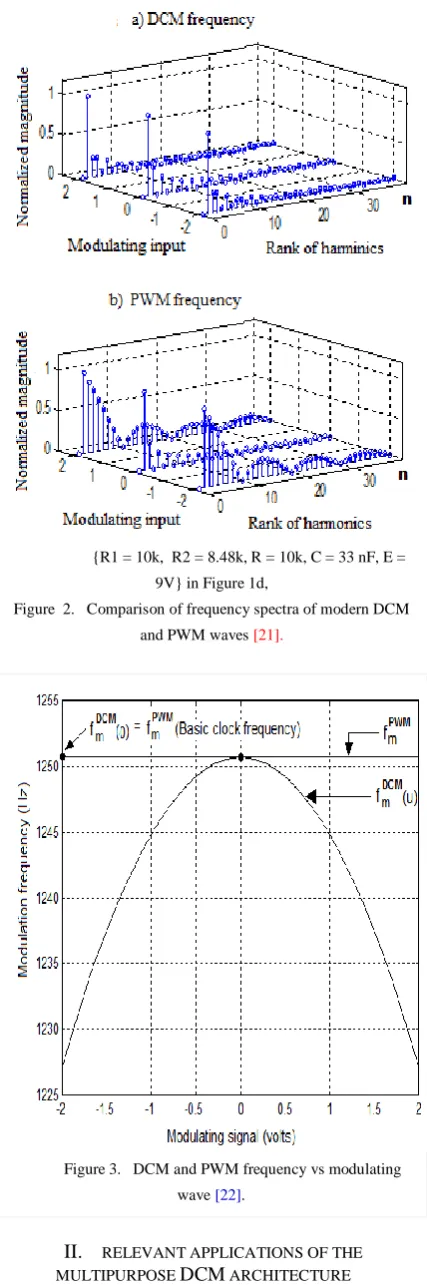
From Fig. 1, it is worth noting that the multipurpose DCM architecture, offers numerous structural novelties, e.g., embedded modulation clock,
minimum building devices, genius combination of positive and negative feedback loops. It also offers relevant operational properties, e.g., rapid convergence of the frequency spectrum compared to that of a PWM wave as shown in Fig. 2 [21], convex modulation frequency fm(x) as shown in Fig. 3 [22]. Therefore, the
Review of a Multipurpose Duty-Cycle Modulation Technology in Electrical and Electronics Engineering 11
II. RELEVANT APPLICATIONS OF THE MULTIPURPOSE DCM ARCHITECTURE
The multipurpose DCM architecture, has been used in a number of application areas. The set of relevant areas to be reviewed consists of DCM-based instrumentation systems (i.e., DCM-based ADC, DCM-based DAC), DCM-based power electronic converters (i.e. DCM-based Buck power converters,
DCM-based Boost power converters, DCM-based power inverters), and DCM-based digital signal transmission systems.
A. DCM-Based ADC systems
Following a pioneering paper published in 2005
[19], many research works have been conducted on the use of DCM architecture, for building novel DCM-based ADC schemes [23-26]. The first single channel DCM-based ADC system has been initiated in [23], where the well tested workbench built for the sake of experimental validation, is presented in Fig. 4a. It consists of a PC equipped with a DCM module, a LPT data acquisition board, a Visual Basic application developed for simultaneously sampling, acquiring, and filtering the DCM sampled data under 50 Hz modulating bandwidth. On the other hand, Fig. 4b deals with a well tested m-channels DCM-based ADC system [24]. The DCM parameters used in both prototyping systems were {R1 = 10k, R2 = 8.2k, R =10k , C=33 nF , Vcc = 9 V}, with fm(0) = 1.47 KHz (basic modulation frequency), fs = 50 kHz (sampling frequency), fbw = 50 Hz (modulating bandwidth).
{R1 = 10k, R2 = 8.48k, R = 10k, C = 33 nF, E = 9V} in Figure 1d,
Figure 2. Comparison of frequency spectra of modern DCM and PWM waves [21].
Figure 4. Workbench : (a) PC-based DCM-ADC [23]; (b) DSP/FPGA-based DCM-ADC [24]. Figure 3. DCM and PWM frequency vs modulating
It is worth noting that in a multichannel DCM-based ADC presented in Fig. 4(b), it is unnecessary to use an external multiplexing device for sequentially capturing and sampling a set of m duty-cycle modulated waves, since a single digital m-bit input port can simultaneously handle m DCM channels. However, each sampled DCM signal is associated with a corresponding IIR (infinite impulse response filter) filter, and the whole set of m IIR filters are processed and monitored simultaneously by an embedded Visual Basic routine. Although it is an intractable task to achieve higher frequency modulating bandwidth under real time programming within Windows platform, the merits of the first PC-based workbenches as shown in Fig. 4, have been to prove the real time feasibility of the DCM-based ADC architecture in industrial instrumentation engineering.
In recent research works [27-28], the modern DCM-based ADC architecture, has been designed, implemented and well tested. In [27], an optimal FPGA-based DCM-ADC architecture has been designed, and implemented under Xillinx system generator.
Then, in [28], a complete FPGA-based DCM-ADC has been designed, built and well tested using a hardware co-simulation platform as shown in Fig. 5. It consists of a PC/Laptop equipped with appropriate software tools (Matlab/Simulink, Simulink/Xilinx system generator, and Xilinx ISE development software), and a FPGA kit connected to the PC by a JTAG cable. As a result, for 3 KHz modulating bandwidth, fm(0) = 172 KHz (modulating frequency) and 25 KHz oversampling frequency, high quality experimental ADC data have been acquired, and the normalized characteristics obtained were SNR = 49.55 dB, SFDR = -41.19 dB, and Noise Floor Range = -140 dB.
B. DCM-Based DAC systems
The general principle of DCM-based DAC presented in Fig. 6, is to transform a digital modulating wave {x(k T)}, into a bit-stream of DDCM (digital DCM) wave xm(k T) ≡ xm(x(k T)), in
order to reconstitute the corresponding analog signal x(t) from the sample of xm(k T) using a well designed
low pass filter. The DDCM system being a PC [29-31] (initially used in 2012 for feasibility tests under Windows from a Visual Basic application program), a microcontroller [21] or a FPGA [31-32].
Figure 6. General principle of DCM-DAC.
In the microcontroller-based DCM-DAC system initiated in [21], the upstream DDCM block was designed and implemented as a FFT (fast Fourier series) module for the sake of rapid digital processing. The FFS concept was motivated by the rapid convergence of the DCM frequency spectrum, compared in similar operating conditions to that of the PWM as recalled earlier in Fig. 2 [21].
Figure 5. Co-simulation hardware environment for
FPGA-based DCM-ADC [28]
Review of a Multipurpose Duty-Cycle Modulation Technology in Electrical and Electronics Engineering 13
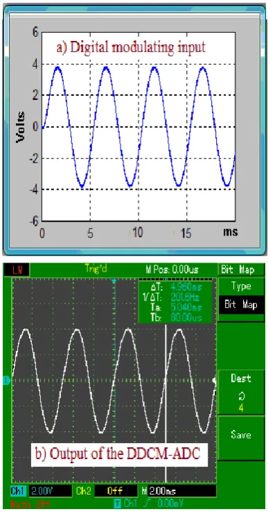
The workbench used in this case to build and test the merit of the prototyping DCM-based DAC, is presented in Fig. 7, where fbw = 200 Hz (modulating bandwidth), fm(0) = 29 KHz (basic DCM frequency), fs = 500 KHz (sampling frequency), R1 = 47k, R2 =18k , R3 = 27k , R4 = 15k, R5 = 1k , C1 = 6.8 nF, C2 = 10 nF. This workbench consists of a PC with the installed tools (e.g;, Microchip MPLAB X IDE XC16 compiler, USB DsPIC30F6014A development Kit with 20 MHz clock, external analog filtering module, and LW2042C digital storage oscilloscope with 40 MHz bandwidth). A sample of virtual simulation and experimental results obtained when testing the workbench is presented in Fig. 8 [21]. It is worth noting that the DDCM-ADC response for a digital modulating sine input (4 V, 50 Hz) observed in Fig. 6a, is a high purity analog sine wave shown in displayed in Fig. 8b, as displayed on the screen of a digital memory storage oscilloscope.
In a further enhanced FPGA-based workbench used in [31] and shown in Fig. 9 where fbw = 3 KHz (modulating bandwidth) and {R1 = 10k, R2 =1k , R3 = 2.2k , R4 = 10k , R5 = 1k , C1 = 10 nF, C2 = 2.2 nF, E = 9 V}, the DDCM algorithm was implemented using a DDCM look up table associated with Digital
duty-cycle function Dcm(x). The relevant results observed in Fig. 10 shows the purity of the output signal of a DCM-based DAC.
Fig. 10 shows the high quality of simulated and experimental results, obtained in [31] for both digital modulating sine and triangle input signals.
Furthermore, a FPGA-based multichannel DCM-based ADC version has been developed and well tested in [31]. Fig. 11 shows the workbench architecture and main results of the prototyping multichannel DCM-based ADC system, where fm(0) = 172 KHz (basic DCM modulation frequency), and fs = 25 MHz (DCM sampling frequency), and R3 Figure 8. Virtual simulation and experimental results of the
FF-Based DDCM-ADC [21]
SFDR = 40 dBc, FPGA resources < 1%
Figure 9. FPGA-based workbench of DCM-based DAC and a sample of results [31].
(a) Simulated, (b) experimental Figure 10. Sample of results for digital modulating
=2.2k, R4 =10k, R5 =1k , R6 =18k, C1 = 10 nF, C2 = 2.2 nF.
The algorithmic flowchart of the multichannel case, resulted from that of a single channel DCM-based ADC [31], by just migrating target scalars quantities into vectors for independent and simultaneous operating conditions. As an implication, a single m-bit output port of the FPGA was sufficient to drive m independent DDCM bit streams outputs, each of which been associated with a terminal low pass filter required, for reconstituting the analog waveform of the modulating wave encapsulated in the related DDCM bit-stream.
C. DCM-BASED DRIVERS FOR POWER DC-DC
SYSTEMS
Historically speaking, the PWM is the most popular technology of drivers for power electronics systems. Surprisingly, many growing innovative ideas on PWM schemes, are limited to the enhanced PWM architectures to be developed or to be embedded into advanced DSP chips. However, following recent comparative studies between DCM and PWM principles as preliminary outlined in Fig. 1, the modern DCM technology might become a potential innovative candidate, for the design of optimal control drivers in power electronics engineering.
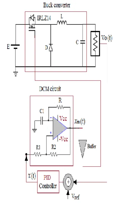
The feasibility and realistic nature, as well as the high quality of DCM-based control drivers for DC-DC power converters, have been outlined in recent research works for Buck and Boost power converters in [33] and [34] respectively.
The first novel DCM-based control structure for Buck power converters as shown in Fig. 12, was initiated in [33], where the basic modulation frequency of the DCM circuit was fm(0) = 30 KHz, i.e., { R1 =1.2k, R2 =10k , R =2.32k , C1 =33 nF, Vcc = 15 V}. In addition, the set of parameters used in the power electronics part was {L = 1 mH, C = 220 μF, Ro = 0.0033k (output load)}. The prototyping control system was well tested and compared in theory and practice to a PWM-based control scheme with the same operating conditions, i.e., power Buck converter, PID Feedback controller and basic modulation frequency for fPWM = fDCM (0) = 30 KHz
since fDCM (x(t)) is a convex function.
The pioneering nature of DCM structure in [33], revealed attractive findings, e.g., a) fast decreasing frequency spectrum of the modulated wave; b) convexity of the duty cycle function Dm(x); c) higher quality under the same open-loop and feedback control loop conditions.
The DCM-based control architecture for power Boost converters shown in Fig. 13, was
Performance: 10-12 bit resolution per channel, FPGA resources < 30%
Figure 11. FPGA-based workbench of multichannel DCM-based DAC and a sample of results [32].
Review of a Multipurpose Duty-Cycle Modulation Technology in Electrical and Electronics Engineering 15
studied in [34-35]. In [34], the set of parameters
used was {R1 =1.2k, R2 =10k , R =1.2k , C1 =3.3
nF, Vcc = 15 V, L = 1 mH, C = 470 μF, Ro = 0.015k
(output load)}, and the great emphasis was on the design of the DCM circuit as well as an analog PID controller required to meet the
desired closed loop specifications. In [35], the
equivalent discrete feedback control systems was designed and validated, using a virtual prototyping platform.
D. DCM-BASED CONTROL ARCHITECTURE FOR SINGLE PHASE POWER INVERTERS
Fig. 14 shows the DCM-based control scheme studied recently in [36], for single phase power inverter systems. In the well tested prototyping system, the basic modulation frequency of the DCM circuit input was fm(0) = 20.24 KHz corresponding to the set of parameters {R1 =10k, R2 =8.2k , R =10k , C1 =2 nF, Vcc = 12 V}, associated with the following parameters used in the power electronics
part { RL = 0.15 - 0.25k, L = 150 mH, C = 66 μF, R0 = 0.250k}. For this set of simulation data, numerous results obtained under open loop and PID feedback control, have been very satisfactory. The design and implementation of the feedback control of the whole DCM-based power inverter, are interesting problems to be completely solved soon.
E . DCM-Based digital transmission systems
The DCM-based digital transmission scheme presented in Fig. 15a, was recently modelled, characterized, simulated and well tested in [37].
The prototyping system consists of a virtual AWG (arbitrary waveform generator), a DCM circuit with parameters {R1 = 1k, R2 =9k, R = 5k , C1 =5 nF, Vcc = 15 V}, a lossless transmission line with parameters {d = 1 Km (length), sqrt(L x C) x d = 0.009 s (line delay}, and a 2nd order analog filter with transfer function F(s) = 12764 / (22757e-7 s2 +15 s +10000). Figure 13. DCM-based control architecture for power
Boost converters [34-35].
Fig. 15b shows a sample of high quality results associated with the transmission of a modulating chirp waveform signal. Indeed, additional simulation results obtained under the same operating conditions,
indicated that the DCM-based digital transmission line can safety support a wide range of arbitrary waveforms.
III. STATE –OF-ART EVALUATION OF APPLICATIONS OF THE MULTIPURPOSE DCM TECHNOLOGY
Even though the multipurpose DCM technology was initiated earlier in 2005 for solving instrumentation problems, its potential applications, as multipurpose building drivers for a variety of dynamic control systems, started later from 2012. Fig. 16 shows the evaluation results of most relevant research works ([19-37]) published since 2012, on pioneering applications of the multipurpose DCM architecture.
From Fig. 16, it is clear that since 2012, the multipurpose nature of DCM architecture, has increasingly motivated pioneering research works, addressed to electrical and electronics engineering. In addition, it is clear also that these research works are not uniformly distributed over the set of application areas, since the earlier an application area is explored, the higher the resulting number of works conducted over time. In any application area considered in Fig. 16, the related research works were limited to the test of basic DCM-based architecture and systems. However, as detailed in the next section related to future research opportunities, it would be possible to extend the aforementioned works if more greedy needs are required.
IV. FUTURE RESEARCH OPPORTUNITIES
The future of the multipurpose DCM technology will be dictated in each application area, either by the development of enhanced DCM architecture as it had been the case for other types of switching modulation architectures (i.e., PWM, SDM and classical DCM), or by of the use of embedded DCM technology as on-chip drivers for novel and patentable products dedicated to the electrical and electronics engineering markets. Indeed, the instrumentation engineering sector might be potentially impacted by the Figure 15. DCM-based digital transmission of analog
AWS [37].
Review of a Multipurpose Duty-Cycle Modulation Technology in Electrical and Electronics Engineering 17
development of innovative multichannel DCM-based ADC boards, multichannel DCM-based DAC boards, as well as multichannel DCM-based virtual AWG (arbitrary waveform generators). On the other hand, potential business opportunities might grow fast, from the development of multichannel DCM-based drivers, with embedded versions into microchips (e.g. microcontrollers, FPGA and CPLD) for power electronics converters and robotic control systems. Another potential research field to be investigated in the future, will rely on DCM-based digital signal transmission systems, via optic fiber media and protocols.
V. CONCLUSION
A complete history of DCM control technology as presented in this review paper, could be divided into three relevant time periods, i.e., 1962-2005, 2005- 2012 and 2012-2018.
From 1962 to 2005, the DCM technology invented for solving digital transmission problems of analog signals, was characterized by a greedy architecture. Then, from 2005 to 2012, the great emphasis of unpublished scientific works conducted in the research team of the authors of this review, was on the discovery and in-depth understanding of intrinsic virtues offered by the multipurpose DCM architecture. Furthermore, from 2012 until today (2018), the DCM architecture has been successfully used as an optimal building technology of both analog or digital drivers, for a variety of basic dynamic control systems.
Finally, the emergency of DCM technology in electrical and electronics engineering, will be motivated in each application area, by the use of DCM-based drivers when building more complex dynamic control systems, or by the development of enhanced on-chip versions of DCM-based drivers, in order to meet greedy requirements of nanotechnology instrumentation and control systems in electrical, electronics and communication engineering.
AUTHORS CONTRIBUTIONS
Leandre Nneme Nneme contributed to the synthesis of research papers on DCM-based ADC, DCM-based drivers for power electronics converters, and DCM-based digital signal transmission systems.
Bertrand Lonla Moffo contributed to the synthesis of research papers on DCM-based DAC, with applications on single and multichannel virtual instrumentation systems.
Gisele Beatrice Sonfack contributed to the synthesis of research papers on optimal DCM-based ADC systems and their applications.
Jean Mbihi contributed to the comparative studies of switching modulation technologies (i.e., PWM, SDM, classical DCM and multipurpose DCM), and to the state-of-art evaluation and to the synthesis of future research opportunities about the multipurpose
DCM architecture. He also supervised the edition and corresponding activities of this review article.
REFERENCES
[1] E. Rosa, “Analog-to-digital conversion via duty cycle modulation.” IEEE transactions on circuits and systems : Analog digital signal processing, , volume 44, No 11, pp. 907-914, 1997.
[2] Wikipedia, Pulsewidth modulation https://everipedia.org/ wiki/Pulse-width_modulation/, accessed on 08 August 2018.
[3] G. E Heftman. “Power Electronics, PWM: From a single Chip to a giant industry.” 2005 https://www.powe relectronics.com/power-management/pwm-single-chip-giant-industry, accessed on 05 August 2018.
[4] S. Sandip Kumar, Harish Kumar; Kamal Singh and Amit Patel. “A survey and study of many types of PWM techniques used in induction motors drive.” International Journal of engineering Sciences & advanced technology., volume 4, Issue 1, pp. 18-22, 2014.
[5] D. Baimel, S. Tapuchi and N. Baimal, “A review of carrier based PWM techniques for multilevel inverters control.” WSEAS Transactions on power systems, volume 12, pp. 165-170, 2017.
[6] ,M. A. Boostand and P. D. Ziogas, “State-of-the art carrier PWM techniques : A critical review evaluation.” IEEE transactions on industry applications, volume 24, Issue 2, ,pp. 271-280, 1988.
[7] R. B. Sidney, “Advanced regular-sampled PWM control techniques for drives and static power converters.” IEEE transactions on Industrial Electronics, volume 24, No 4, pp. 367-373, 1995.
[8] D. Grahame Holmes and T. O Lipo, “Pulse width modulation for power converters : Principles and practice.” Wiley-IEEE Press, 2003, 744 pages.
[9] C. C. Cuttler, “Transmission system employing quantization.” U.S. Patent 2,927,962, April 26, 1954, issued March 8, 1960. [10] H. Inose, Y. Yasuda and J. A. Murakami, “A telemetering
system by code modulation: Sigma-Delta modulation.” IRE transactions on space electronics telemetry, volume SET-8, pp. 204-209, September 1960.
[11] D. J. Goodman, “The application of Delta modulation of analog-to-PCM encoding.” Bell system technical journal,
volume 48, February 1969.
[12] N. S. Jayant, “Waveform quantization and coding.” IEEE press and John Wiley, 1976, ISBN 0-471-01970-4.
[13] M. W. Hauser, “Principles of oversampling A/D conversion.” Journal Audio Engineering Society, volume 39. pp. 3-26, February 1991,
[14] Shreier, R; Temes, G. C., Understanding Delta-Sigma data converters. Wiley-IEEE Press, November 2004, ISBN 0-471-46585-2
[15] Biad, J. R.; Richardson, T. Duty cycle modulated multivibrator. U.S. patent 3,037,172, May 29, 1962. [16] P. H.. Harvey, and N. H. Hampton Falls, Transmitting a
signal using duty cycle modulation. U.S. Patent 6,111,680, August 29, 2000.
[17] O. K.. Yoon, I. A. Zuleta, J. R. Kimmel, M. D. Robins, and N. R. Zare, “Duty cycle and modulation efficiency of two channel Hadamard Transform Time-of-Flight mass spectrometry.” Journal of the American society for mass spectrometry, volume 16, No 11, pp. 1888-1901, November 2005.
[18] F. J Delozier, Digital transmission of analog signals, WJ Tech-note, © WJ communications Inc., 2001. http://www.
rfcafe.com/references/articles/wj-tech-notes/digital-transmission-analog-signals-v8-5.pdf, accessed on 08 August 2018.
[20] J. Mbihi, “Dyanmic modelling and virtual simulation of digital duty cycle modulation control drives”. International Journal of Electrical, Computer, Energetic, Electronic and Communication Engineering. © WASET (World Academy of Science, Engineering and Technology). volume 11, No 4, pp. 472-477, 2017.
[21] B. Moffo Lonla, J. Mbihi, L. Nneme Nneme, and M. Kom, “A novel digital-to-analog conversion technique using duty cycle modulation.” International Journal of circuits, systems and signal processing. volume 7, Issue 1, pp. 42-49, 2013. [22] B. Moffo Lonla, J. Mbihi, and L. Nneme Nneme, “Low cost
and high quality duty cycle modulation scheme and apllications.” International Journal of Electrical, Computer, Energetic, Electronic and Communication Engineering. © WASET (World Academy of Science, Engineering and Technology). volume 08, No 3, pp. 472-477, 2014.
[23] J. Mbihi, F. Ndjali Beng, M. Kom and Nneme Nneme, “A novel analog-to-digital conversion scheme using nonlinear duty cycle modulation.” International Journal of Electronics and computer science engineering, volume 1, No 3, pp. 818-825, 2012.
[24] J. Mbihi, F. Ndjali Beng , M. Kom, and L. Nneme Neme, “A multichannel analog-to-digital conversion technique using parallel duty cycle modulation.” International. Journal of Electronics and computer science engineering. volume 1, No 3, pp. 826-833, 2012.
[25] J. Mbihi and A. Motto, “ Mesures par ordinateur des signaux modulés en rapport cyclique.” Chapter 5 in Instrumentation virtuelle assistée par ordinateur, pp. 68-82, Ellipses Editions, Paris, France 2012.
[26] J. Mbihi and A. Motto, “ Oascilloscope virtuel multicanaux à modulation en rapport cyclique.”, Chaper 6 in
Instrumentation virtuelle assistée par ordinateur, pp. 84-98, Ellipses Editions, Paris, France 2012.
[27] G. B. Sonfack,. J. Mbihi and B. Moffo Lonla, “Optimal duty-cycle modulation scheme for analog-to-digital conversion systems.” International Journal of Electronics and communication engineering, © World Academic of Science, Engineering and Technology, volume 11, No 3, pp. 354-360, 2017.
[28] G. B. Sonfack and J. Mbihi, . “FPGA-based analog-to-digital conversion via optimal duty-cycle modulation”. Journal of Electrical and Electronics Engineering, volume 8, No 2, pp. 29-38, 2018.
[29] J. Mbihi and A. Motto, “ Conversion numérique-analogique par modulation en rapport cyclique.” Chapter 11 in
Instrumentation virtuelle assistée par ordinateur, pp. 148-155, Ellipses Editions, Paris, France 2012.
[30] J. Mbihi and A. Motto, “Générateur de signaux virtuels à modulation en rapport cyclique. ” Chapter 12 in
Instrumentation virtuelle assistée par ordinateur, pp. 84-98, Ellipses Editions, Paris, France 2012.
[31] B. Moffo Lonla and J. Mbihi,. “A novel digital duty-cycle modulation scheme for FPGA-based digital-to-analog conversion.” IEEE transactions on circuits and systems II, volume 62, No 6, pp. 543-547, June 2015.
[32] B. Moffo Lonla, J. Mbihi, J. and L. Nneme nneme, “FPGA-based multichannel digital duty cycle modulation and application to simultaneous generation of analog signals.” “STM Journal of Electronic Design Technology, volume 8, Issue 1, pp. 23-35., 2017.
[33] J. Mbihi L. Nneme Nneme, “A novel control scheme for buck power converters using duty cycle modulation.” International Journal of power electronics, © Inderscience Enterprises Ltd, volume 5, No 3/4, pp. 185-199, 2013. [34] Y. P. Dangwe sounsoumou, Haman-Djalo; J. Mbihi and J.
Y. Effa, “Modélisation et simulation virtuelle d’un nouveau schema de réglage de hacheurs boost à commande rapprochée par modulation en rapport cyclique.” Afrique Sciences, Volume 13, No 1, pp. 176-185, 2017.
[35] Y. P. Dangwe sounsoumou, J. Mbihi, Haman-Djalo; and J. Y Effa,. “Virtual digital control scheme for duty cycle modulation boost converter.” Journal of Computer Science and Control Systems, Volume 10, No 2, pp. 22-27, October 2017.
[36] A. Obono Biyobo, L. Nneme Nneme and J. Mbihi, “A novel sine duty cycle modulation control scheme for photovoltaic single phase power inverters.” WSEAS Transactions on Circuits and Systems, volume 17, pp. 107-113; 2018, [37] L. Nneme Nneme and J. Mbihi, “Modeling and simulation
![Figure 1. Summary of the comparative study among PWM, DSM, classical DCM and multipurpose DCM technologies [19-20].](https://thumb-us.123doks.com/thumbv2/123dok_us/7806211.2085126/2.595.67.504.76.643/figure-summary-comparative-study-pwm-classical-multipurpose-technologies.webp)


![Figure 15. DCM-based digital transmission of analog AWS [37].](https://thumb-us.123doks.com/thumbv2/123dok_us/7806211.2085126/8.595.73.264.67.698/figure-dcm-based-digital-transmission-analog-aws.webp)
