HDL Design for Peta Hertz Clock Based 2e7-1 Peta Bits
Per Second (P.b.p.s) - PRBS IP Core Generator For Ultra
High Speed Wireless Products
Prof.P.N.V.M Sastry
Dean-Engineering IT EDA S/W, R&D-CELL & E.C.E J.B.R.E.C, Moinabad, R.R.Dist.Hyderabad-75, India
Prof.Dr.D.N.Rao
Principal J.B.R.E.C, Moinabad R.R.Dist.Hyderabad-75, IndiaDr.S.Vathsal
Dean- R&D, EEE J.B.I.E.T, Moinabad, R.R.Dist. Hyderabad-75,
India
ABSTRACT
The Design is mainly Intended for High Speed Random Frequency Carrier Wave Generator of 1 Peta Bits Per Second Pbps Data Rate using 2e7-1 Tapped PRBS Pattern Sequence. The PRBS is Designed by using LFSR Linear Feed Back Shift Register & XOR Gate with Specific Tapping Points as per CCITT ITU Standards. RTL Design Architecture Implemented by using VHDL &/ Verilog HDL, Programming & Debugging Done by using Spartan III FPGA Kit. Transmission done through this carrier frequency. Propagation Carrier Done either Serially / Parallel lines I/O.
Keywords
CCITT – Consulting Committee for International Telegraph & Telecom , ITU – International Telecom Unit, RTL- Register Transfer Level, LFSR-Linear Feedback Shift Register, VHDL- Very High Speed Integrated Circuit Hardware Description Language, PRBS-Pseudo Random Binary Sequence.
1.
INTRODUCTION
Transceivers Designed for Hi-Fi Wireless Internet Data Packets Computing and Cloud Computing etc. Transmission, Reception of Data is in the RANDOM Sense, This PRBS Generator, Receiver is Designed for Identification property of Different Tapped PRBS Sequences like 7, 10,15,23,31 at a Clock carrier frequency speed of Tbps/Pbps. The Length of PRBS sequence is 2L-1. 2L-1 times repeated the sequences. this is mainly suit for multiple users to transmit and received data in accurate time for very long distance communications like GPS Data Acquisition, GSM Communication Systems, WiFI,GiFI,LTE, Wireless OFDMA , CDMA,QCDMA Computing, wireless internet computing, cloud computing etc because of Ultra High speed Communication Rate in terms Gbps,Tbps,Pbps . All these PRBS LFSR Sequences are designed by tapping different points according to ITU O.150,O.151,O.152 Standards. This PRBS Design Consists of Multiplexer, PRBS Registers of different tapped sequence points, Clock Frequency Generators of Pbps Speed. The Advantages of these PRBS Generators having In Built Checkers, Bit Error Rate Detection & Correction by using PRBS Checkers. These are simply Linear Polynomial Checkers & CRC.
Fig 1: PRBS DESIGN -Fibonacci (many-to-one) realization of LFSR with minimum number of taps and XOR gate in its feedback.
2.
2E
7-1 PETA BITS PER SECOND (PBPS) PRBS DESIGN
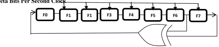
Peta Bits Per Second Clock
Fig 2: 2e7-1 Pbps PRBS DESIGN
1.1
2e
7-1 Pbps PRBS Design Description
The 2e7-1 Pbps PRBS Generator Consists 8-Bit Linear Feed Back Shift Register and XOR Logic Gate and operation clock frequency of the PRBS is Peta Hertz, Baud rate of generation is Peta Bits per Second. Tapping Done through XOR Logic Gate , tapping elements 7 and 6 are the feedback inputs to the XOR Gate, XOR Gate Compare the tapping points and generate the output, the output is feedback in to the input of 8 bit Shift Register, tapping elements 7 and 6 are standardized as per CCITT – ITU O.150 , The PRBS Generates Randomized Repeated Data Sequence Patterns called
n-bit shift register
“SEED WORD” for High Frequency Digital Carrier Wave Frequency , the frequency rate is 1 Peta Bits Per Second . Peta bits Per Second Clock Generated by Peta Clock Generator 250 Clock Cycles per one Peta Clock Cycle. These are used for Very useful for Long Distance wireless & Telecom Products and Applications.
3.
VLSI IC INDUSTRIAL EDA SOFTWARE DESIGN FLOW CHART
Tape Out IC
Fig 3: VLSI IC Design Flow Chart
1.2
Description
The Industrial Standard EDA Software Design Flow Chart is mainly used for Implementation of ASIC Design in Soft Flow , and for Delivery of Any ASIC ,SOC Products, It Consists the following design flow phases as per Quality VLSI EDA IC Software Standards, Design Entry, HDL Coding, Simulation, Synthesis , Floor planning, Placement & Routing, Configuration, after that Tape out process done. In this 2e7-1 PRBS Design , enter the design architecture specifications using Design Entry phase, Verilog HDL & VHDL Coding Done by using RTL HDL Coding, and Running the functionality of the design done simulation phase, Abstract soft HDL Description into Hardware Gate Level Net List Done Synthesis Phase, Planning the PRBS Design Location on FPGA LUT done by Floor planning Phase, PRBS Design Placement and Routing Done on Xilinx Soft FPGA IP Core Spartan-III FPGA at Peta Hert Clock Frequency using Xilinx ISE 9.2i IDE Software.
DESIGN ENTRY
HDL CODING
SIMULATION
FlOOR PLANNING
PLACEMENT
ROUTING
4.
DESIGN FLOW REPORTS
4.1 2e
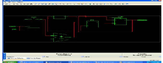
7-1 Pbps PRBS DESIGN RTL BLOCK
Fig 4: 2e7-1 Pbps PRBS DESIGN RTL
4.1.1 2e
7-1 Pbps PRBS RTL Description
The PRBS RTL Block is the Top Level Block Contains IO Block and Internal Design Functional Block , The I/O Specifications are Pbps Clock, reset, PRBSout[7:0] Data Out;
4.2 2e
7-1 Tbps PRBS RTL Schematic Design
4
.3 2e
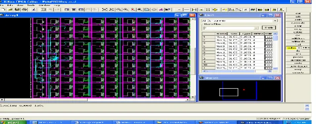
7-1 Pbps PRBS Design Placed Report
Fig 5: 2e7-1 Pbps PRBS XC 3S 200 TQ 144 FPGA DESIGN Placed Report
4.4 2e7-1 Pbps PRBS Design Routed Report
Fig 5: 2e7-1 Pbps PRBS XC 3S 200 TQ 144 FPGA DESIGN Routed Report
Fig 6: 2e7-1 Pbps PRBS Simulation Results
1.3
Description Of Simulation
The 2e7-1 Pbps PRBS generates 8 bit High Speed Repeated Random Sequence Patterns called “Seed Words” in the form of High Frequency Carrier Wave Generated patterns at the frequency rate of 1 Peta Hertz, Baud Rate Speed is Peta Bits Per Second. This Simulation Wave form editor contains Clock Input and Reset Input, 8 Bit PRBS Data Out.
6.
CONCLUSION
Designed 2e7-1 Tbps PRBS for Ultra High Speed Wireless Communications, This Design is mainly intended for Very High Long Distance Communication at the frequency rate of Peta Bits per Second. And this product is very suited for All Very Advanced Smart Digital Computing Communication Products like Advanced 3G,4G,5G,6G, Hi-Fi Space Communication ,Satellite Communication Products. This product is very suit for even very advanced internet & cloud computing w.r.t speed. Suit for all HiFi Consumer Mobile Applications and Products.
7.
ACKNOWLEDGMENTS
Our thanks to the experts who have contributed towards development of the Design
8.
REFERENCES
[1] Wikipedia, “http://en.wikipedia.org/wiki/ Pseudorandom_binary_sequence” [2] Wikipedia “http://en.wikipedia.org/wiki/ Linear_feedback_shift_register”
[3] SY Hwang, GY Park, DH Kim, KS Jhang, “Efficient Implementation of a Pseudorandom Sequence Generator for High-Speed Data Communications”, ETRI Journal, Volume 32, Number 2, April 2010.
[4] ITU – CCITT Reference Document [1] A Chow, WS Coats, D Hopkins, “A Configurable Asynchronous Pseudorandom Bit Sequence Generator”, 13th IEEE International Symposium on Asynchronous Circuits and Systems (ASYNC 07), Page(s): 143 - 152, March 2007.
[5] Xilinx Data Sheet XAPP884 (v1.0) January 10, 2011
BIBLIOGRAPHY – AUTHOR PROFILE
Prof.P.N.V.M Sastry
Currently working with a Capacity of Dean- IT EDA Software – R&D CELL & ECE DEPARTMENT, He Did Master Degree In Science- M.S Electronics, Under Department Of Sciences, College Of Science & Technology AU -1998.Did PG Diploma In VLSI Design From V3 Logic Pvt Ltd B’Lore-2001, Did M.Tech (ECE) From IASE Deemed University2005. Currently Pursuing (PhD)ECE(VLSI) , JNTU Hyderabad-2012 , Over Past 16 years of Rich Professional Experience with Reputed IT Software
Industrial MNC’s, Corporate –CYIENT (INFOTECH), ISiTECH as a world top keen IT
Industrial Software Specialist – World Top Software Engineering Team Leader(Level 6) Eng-Eng- HCM
Electronics Vertical & Program Manager – MFG I/C,EDS,BT,NON BT Embedded Software ,Avionics & Automotive Hi-tech Software Engineering Verticals & Departments , Program Lead – Embedded & VLSI & Engineering Delivery Manager – IT Semiconductor Software Engineering Vertical ,at ISiTECH , also worked with Govt R&D, Industrial Organizations, Academic Institutions of Comparative Designations & Rolls . His Areas Of Interest are VLSI –VHDL, Verilog HDL, ASIC, FPGA & Embedded Software Product Architectures Design & Coding Development .He mentored & Architecting Various Real Time, R&D ,Industrial Projects/Products related to VLSI & Embedded System Software & Hardware.. His Key Achievements are Participated Various Top Class International IT MNC Delegates Board Meetings, IT Software MNC Board Meetings(Tier1/2 Level MRM-VP,COO Level) , Guided R&D ,Industrial , Academic Projects /Products –VLSI-ASIC,FPGA & Embedded & Embedded,VLSI Software Project &/ Program Management & Also Coordinated Various In House & External IT Project Workshops & Trainings At CYIENT( INFOTECH) as a I/C- MFG Eng Software Vertical , Also Participated Various National R&D Workshops, FESTS, FDP’s &Seminars. Recently He Published Various national & International Journals. He has attended as a Judge for IEEE Paper Presentation conducted By C.B.I.T ,2010. and also attended as a Judge for various paper and poster presentations of various national conferences conducted by various prestigious engineering institutions.
Dr. D.N Rao
B.Tech, M.E, Ph.D, principal of JBREC, Hyderabad. His carrier spans nearly three decades in the field of teaching, administration,R&D, and other diversified in-depth experience in academics and administration. He has actively involved in organizing various conferences and workshops. He has published over 11 international journal papers out of his research work. He presented more than 15 research papers at various national and international conferences. He is Currently approved reviewer of IASTED International journals and conferences from the year 2006. He is also guiding the projects of PG/Ph.D students of various universities