In search of triplet
superconductivity in lateral cobalt
Josephson junctions
THESIS
submitted in partial fulfillment of the requirements for the degree of
MASTER OF SCIENCE in
PHYSICS
Author : Menno L. Pleijster
Student ID : s1319582
Supervisor : prof. dr. J. Aarts
Daily supervisor: MSc. K. Lahabi
2ndcorrector : dr. M. de Dood
In search of triplet
superconductivity in lateral cobalt
Josephson junctions
Menno L. Pleijster
Huygens-Kamerlingh Onnes Laboratory, Leiden University P.O. Box 9500, 2300 RA Leiden, The Netherlands
17th February 2016
Abstract
Triplet superconductivity in lateral Josephson junctions has only been shown in the ferromagnet CrO2. We succeeded in creating a disk-shaped lateral cobalt Josephson junction with a trench width
below 20 nm. The device shows promising signs of superconducting triplet correlations. For exchange fields up to 15 mT we see an increase in the critical current, possibly caused
by an increase of the magnetic non-collinearity as the Ni generating layer aligns with the field. We also observe oscillations
in the critical current. These oscillations have a period of approximately 4 mT and are believed to be the result of a flux
Contents
1 Motivations 7
2 Introduction and theory 9
2.1 Superconductivity and Magnetism 9
2.2 Proximity effect 11
2.3 Triplet mixing 14
2.4 Magnetic inhomogeneity 14
2.5 Josephson junctions 16
3 Lateral cobalt Junctions 19
3.1 Lateral junctions 19
3.2 Magnetic coupling 19
3.3 Magnetic inhomogeneity in a disk 21
4 Nanofabrication 25
4.1 Design 25
4.2 Design requirements 26
4.3 Fabrication steps 27
4.3.1 Sputtering of multilayer structure 27
4.3.2 Focused Ion Beam (FIB) milling 28
4.4 Verifying trench depth 30
5 Results 35
5.1 Superconducting samples 35
5.2 Critical current 39
5.3 Resistance 41
6 CONTENTS
6.1 Oscillations 45
6.2 Cobalt disk 47
6.3 Triplet superconductivity 48
7 Conclusion and outlook 51
6
Chapter
1
Motivations
In the past decade several experiments have shown the presence of a long range superconducting proximity effect in ferromagnets [1, 2]. The major-ity of those results have been achieved in multilayer stacks. Triplet super-conductivity in lateral Josephson junctions has only been reported for the half-metal CrO2[3, 4].
Chapter
2
Introduction and theory
2.1
Superconductivity and Magnetism
Superconductivity is the macroscopic quantum state in which the electri-cal resistance goes to exactly zero. Ever since its discovery in 1911 [5] a lot of effort has been expanded to study this phenomenon, culminating in the explanation of conventional superconductivity in terms of Cooper pairs in the theory by John Bardeen, Leon Cooper and John Schrieffer (BCS) [6]. Followed by the discovery of high critical temperature superconductivity in some cuprate-perovskite ceramic materials in 1986 by Johannes Bednorz and Karl M ¨uller [7].
Practical applications of superconductivity can be found in the form of superconducting magnets, capable of generating very high fields, due to the lack of dissipation in high currents. These magnets find use in any-thing from Magnetic Resonance Imaging (MRI) machines to particle accel-erators. The macroscopic quantum behaviour of superconductors is also used to build extremely sensitive detectors, such as superconducting pho-ton and particle detectors and Superconducting Quantum Interference De-vices (SQUID) to measure weak signals.
10 Introduction and theory
this could be used for example to build dissipationless spin-based mem-ory elements.
Magnetism and superconductivity seems a very paradoxical combination for anyone who has ever witnessed the Meissner effect, in which a station-ary magnet is repelled by a material going through the superconducting transition. A superconductor expels all magnetic fields from its interior by generating dissipationless currents circulating in a plane normal to the field, until a sufficiently high critical field is reached after which all super-conductivity is destroyed∗.
This animosity between magnetism and superconductivity can partially be understood with the BCS theory, where conventional superconductiv-ity is described in terms of Cooper pairs formed by a small attractive inter-action between two electrons with opposite spin. These Cooper pairs exist in the singlet state √1
2|↓↑i − |↑↓i. Since the electrons forming the Cooper pair have opposite spins, the interaction of the electron magnetic moment with any external magnetic field will separate them in energy due to the Zeeman effect and effectively break the Cooper pair, thus suppressing any superconductivity.
Soon after the discovery of the BCS theory it was already discovered that there are two ways to save the Cooper pair and superconductivity in the presence of a magnetic exchange field. While the BCS theory describes Cooper pair singlets with electrons with opposite spins and that have equal but opposite momentum, it was realised in two independent pub-lications in 1964 that the Cooper pair can persist in a non-zero exchange field. The exchange splitting gives rise to two different Fermi surfaces for electrons with up and down spin. This can lead to electron pairings with a centre of mass momentum close to zero, but equal to the Zeeman en-ergy. The non-vanishing momentum leads to a spatially modulated order parameter [9]. This state is called the Fulde–Ferrell–Larkin–Ovchinnikov (FFLO) phase [10, 11].
Alternatively, it is possible to rescue superconductivity in the presence of the Zeeman effect by letting go of the singlet state with opposite spins. A pair of parallel spins|↑↑iand |↓↓i, will not experience Zeeman splitting. While having opposite spins satisfies the Pauli principle, it is not the only possibility. As long as the pair is anti-symmetric state under an overall
∗For type-I superconductors, type-II superconductors start letting in magnetic
vor-tices, until a second higher critical magnetic field value, where superconductivity is com-pletely suppressed
10
2.2 Proximity effect 11
exchange of fermions, the Pauli principle is satisfied. This includes the space, spin, and time coordinates of the two electrons. Thus the electrons can have equal spins, as long as there is a change of sign under exchange of space or time coordinates. The exchange of time coordinates allows for something known as odd-frequency triplet superconductivity [12–15].
While this is a simplified version, and we will delve into the details later in this chapter, superconducting triplet correlations have been discussed for a long time now. In 1974 Berezinskii suggested that an odd-frequency triplet state arises in liquid He3 [12] and was later predicted to arise at Superconducting/Ferromagnetic (S/F) interfaces [16].
This shows that while superconductivity and magnetism seems an odd match at first, their interplay can lead to a lot of interesting physics. A lot of this physics happens on the boundary between a normal superconduct-ing material and a ferromagnet. It is at these interfaces that the proximity effect acts.
2.2
Proximity effect
When a normal metal is in contact with a superconductor, some of the superconducting Cooper pairs will propagate into the normal metal. The distance over which this occurs is determined by superconducting coher-ence lengthξs. The presence of superconducting Cooper pairs in the
nor-mal metal lowers the resistance. In fact when a thin film of a nornor-mal metal is sandwiched between two superconductors (S/N/S) the entire sandwich can go superconducting [17]. This effect is known as the proximity effect.
Alternatively, this can be expressed in terms of Andreev reflections, which describes how a normal current can be converted to a supercurrent. It explains how an electron coming from the normal metal side of an S/N inferface with an energy below the superconducting gap∆can move into the superconductor by reflection of an electron hole into the normal metal with opposite spin and momentum [18, 19]. This is shown in figure 2.1.
When the mean free path of the electronsl is shorter than the coherence length ξs due to scattering, the junction is said to be in the dirty limit.
In this case the superconducting pair will diffuse into the material until a scattering event occurs that breaks the pair. The average distance over which they diffuse is the diffusion length Ld =
q ¯
hD
12 Introduction and theory
Figure 2.1: Andreev reflection: An electron (red) meeting the interface between
a normal conductor (N) and a superconductor (S) produces a Cooper pair in the superconductor and a retroreflected hole (green) in the normal conductor. Vertical arrows indicate the spin band occupied by each particle. Image from Wikimedia [20].
diffusion constant andTdenotes temperature.
Extending the concept of the proximity effect to interfaces between a su-perconducting material and a ferromagnet (S/F) reveals some interesting physics. When a superconductor is placed in contact with a weakly spin-polarised ferromagnet, the singlet Cooper pairs diffusing into the material will experience the exchange field coming from the weak ferromagnet and be broken and thus have a significantly shorter coherence length in com-parison to that in a normal metal.
The presence of the exchange field at the S/F boundary introduces FFLO-phase like behaviour. The exchange field acting on the electrons at the interface will shift the momenta at the Fermi level kF. The electron with
spin up|↑i aligned along the exchange field will find its momentum de-creased by half the Zeeman splittingk↑ =kF−kz/2, while the spin down
electron|↓ifinds its momentum increased k↓ = kF+kz/2. The resulting
centre of mass momentum of the Cooper pair is±kz. As in the bulk
FFLO-phase this implies a modulation in the order parameter of the pair with period 2π/kzwith distancer. This corresponds to a mixture of singlet and
them =0 triplet spin states:
|↓↑i − |↑↓i → |↓↑ieikz·r− |↑↓ie−ikz·r = (2.1)
= (|↓↑i − |↑↓i)cos(kz·r) +i(|↓↑i+|↑↓i)sin(kz·r).
12
2.2 Proximity effect 13
Figure 2.2: The superconducting
pair amplitude of the singlet (green) and triplet (red) with m = 0 pair state around the interface. In the superconducting material on the left (yellow) the singlet pair state is pre-ferred. In the normal metal on the top right the singlet pairs diffuse into the normal metal and slowly decay. No triplet state is formed. In a spin-polarised ferromagnet an FFLO-phase is induced causing an oscillation between the singlet and triplet state. The decay rate of this oscillation is related to the strenght of the exchange field. Image taken from M. Eschrig [8].
The direction of the modulation wave vectorkzmust be perpendicular to
the interface, because only this orientation is compatible with the uniform order parameter in the superconductor.
The difference with the bulk FFLO-phase is that the superconducting cor-relations decay in the ferromagnet with distance from the boundary. The characteristic length scale over which they decay, while modulating, is
ξf =
qD f
Ez in the dirty limit. This strongly decreases with increasing en-ergy of the exchange field Ez. Df is the diffusion coefficient in the
ferro-magnet. This decay length is much shorter than the dirty limit coherence length in the superconductorξs =
q
Ds
2πTc [8, 21], sinceTcis on the order of a few Kelvin, whileEzcan be a few thousand Kelvin. Figure 2.2 shows that
14 Introduction and theory
but will quickly decay in higher exchange fields.
For spintronics highly spin-polarised currents are desired. The rapid de-cay of the supercurrent penetrating into the ferromagnet thus poses a prob-lem. The parallel spin triplet states |↑↑i and |↓↓i with m = ±1 do not experience any Zeeman splitting and are not affected by this decay. The process of triplet mixing, can convert the triplet state withm = 0 into the m=±1 state, solving this problem.
2.3
Triplet mixing
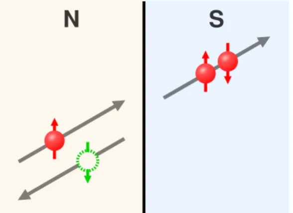
The solution to a long range proximity effect in a ferromagnet, lies with looking at the m = 0 triplet |↓↑i +|↑↓i from a different angle in spin space. The singlet state |↓↑i − |↑↓i is rotationally invariant with respect to the quantisation direction. By changing the quantisation direction the three triplet states change into each other. Image taken from M. Eschrig [8].
In particular, the triplet state|↓↑i+|↑↓iin the y-basis is the parallel spin state i(|↑↑i+|↓↓i) in the z-basis. This is visualised in figure 2.3, where the quantisation direction is changed from two aligned layers to two layers that have a perpendicular magnetization.
2.4
Magnetic inhomogeneity
The generation of equal-spin triplets at the interface depends strongly on the realised magnetic inhomogeneity [22, 23]. In the past decade several methods for realising the required magnetic non-collinearity have been developed.
The first spin triplet supercurrent through the half-metallic ferromagnet CrO2was reported in 2006 [3]. The mechanism responsible for the triplet generation remained unclear, although it was suggested that the necessary magnetic inhomogeneity could come from disorder at the interface. This was later reproduced in 2010 confirming the existence of a triplet proxim-ity effect [4].
An enhanced magnetic inhomogeneity can be achieved in a multilayer of two ferromagnets with perpendicular magnetization direction [22, 24].
14
2.4 Magnetic inhomogeneity 15
Figure 2.3: In (a) |↓↑i+|↑↓i triplets are induced in the superconductor at the
interface. They cannot penatrate into the strongly spin-polarised ferromagnet as the strong exchange field breaks the opposite spin pairs. In (b) a thin layer with a quantisation direction perpendicular to that of the bulk ferromagnet allows the conversion from the|↓↑i+|↑↓itriplet in the y-basis to the equal spin pair
i(|↑↑i+|↓↓i)in the z-basis. These equal-spin pairs are then allowed to extend into the ferromagnet[8].
The experimental realisation of such a S/F/F’ stack is difficult due to cou-pling. Separating the F and F’ magnetic layers with a thin copper layer limits the exhange coupling between the two. The application of a mul-tilayer stack that created a synthetic anti-ferromagnet by sandwiching a thin layer of ruthenium between two layers of cobalt [25] limited the stray fields of the cobalt, minimising the coupling due to stray fields between the F and F’ ferromagnetic layers. In 2009 this showed triplet supercon-ductivity in a cobalt junction [1]. A different multilayer S/F/F’ structure was used in 2012 to generate triplets in CrO2[26].
16 Introduction and theory
As an alternative method of triplet generation by spin-orbit coupling has been suggested [27]†.
Although there are still many barriers to overcome for the full implemen-tation of spin triplet superconductivity in spintronics, there do seem to be viable methods of generating the required triplet pairs. Up to date almost all experiments on triplet superconductivity involve the use of Josephson junctions. As such they are a key stepping stone in understanding triplet superconductivity. Now that we have the means of inducing a triplet prox-imity effect in a ferromagnet, we can use it to send a superconducting triplet current through a Josephson junctions.
2.5
Josephson junctions
A Josephson junction consists of a weak link between two superconduc-tors. While originally describing the quantum tunnelling of a Cooper pair through a thin insulating barrier (S/I/S) [28], it is also applicable to weak physical contacts, such as in a constriction (S/s/S) and due to the proxim-ity effect to weak links consisting of a normal metal (S/N/S) or ferromag-net (S/F/S).
The two equations that govern the Josephson effect are:
U(t) = h¯ 2e
∂φ(t)
∂t (2.2)
I(t) = Icsin(φ(t)). (2.3)
They describe the potentialU(t) over and current I(t) through the junc-tion, where Ic is the critical current of the junction and φ(t) describes the
phase difference between the order parameters in the superconductors on both sides of the junction. The main three resulting consequences are:
• DC Josephson effect
For a fixed phase difference across the junction there will be a direct current flowing through the junction in the absence of any applied field. This current is proportional toIDC = Icsin(φ).
• AC Josephson effect
A constant potential applied to the junction, will cause the phase
†How this would work is beyond the scope of this thesis, as we are relying on
mag-netic inhomogeneity to generate triplets.
16
2.5 Josephson junctions 17
difference to vary linearly in time and result in an alternating current to flow.
• Inverse AC Josephson effect
Applying an alternating potential to the junction results in a DC po-tential that is proportional to the frequency of the applied AC poten-tial. This acts as a perfect frequency to voltage converter. This effect can be used to define the Volt [29].
In the absence of any applied current or potential, in the ground state of the Josephson junction there are two solutions to the Josephson equations that result in no current flowing through the junction. For both a phase of φ = 0 and φ = π this is the case, however the φ = π state turns
out to be unstable and the ground state in a normal S/N/S junction has a phase difference of 0. Some unconventional superconductors do show a phase of π, such as the d-wave superconductor YBCO [30]. These π
Josephson junctions have very unusual properties, as shorting both sides of the junction will result in a spontaneous supercurrent flowing either clockwise or counter-clockwise, decided at random. The flux through such a loop will vary from 0 to 1/2 a flux quantum [21].
This is of particular relevance to m = 0 triplet superconductivity as the presences of the ferromagnet induces the FFLO state, causing the order parameter to oscillate. Depending on the length of the junction this creates either a 0 orπjunction [31, 32].
Josephson junctions can be created out of any weak link in a supercon-ductor, such as a constriction or point contact, but for introducing a ferro-magnetic layer there are two commonly used methods. Multilayer S/F/S structures can be created in either a vertical layered construction, with con-tacts at the top and bottom of the structure, or in a lateral configuration, where the supercurrent flows in the plane of the structure.
Chapter
3
Lateral cobalt Junctions
3.1
Lateral junctions
Lateral junctions have been attempted previously with materials other than CrO2, but so far without any reported success. We investigate the potential limits of the lateral geometry. For spin polarised supercurrents, the relevant parameter for a junction to be proximised is the Spin Diffu-sion Length (SDL). This is the average distance until an event occurs that flips the spin of one of the electrons. Form =1 triplets in the ferromagnet cobalt this distance is of the order of ≥40 nm [34]. It should therefore be possible to construct junctions with lengths of twice the SDL (80-100 nm).
Magnetic non-collinearity is paramount for inducing a triplet supercurrent in any junction. An inability to generate sufficient magnetic inhomogene-ity could stand at the basis of the problems with lateral junctions. This could stem from the difficulty in magnetically decoupling two thin ferro-magnetic layers in close proximity.
3.2
Magnetic coupling
In a strongly spin-polarised ferromagnet them =0 triplet state|↓↑i+|↑↓i decays over atomic distances. To allow triplet mixing at the interface the thickness of the first ferromagnetic layer has to be shorter thanξf.
20 Lateral cobalt Junctions
thickness in thin ferromagnetic films. Thin layers can make very soft fer-romagnets. The presence of a second ferromagnetic layer introduces stray fields to which the first layer strongly couples due to its low coercivity.
Figure 3.1: Micro-magnetic simulations done by Ewout Breukers for a thin 2nm
nickel layer on top off a 45 nm cobalt layer. The simulation shows that the mag-netisation of the thin nickel layer starts to reverse and align anti-parralel to the magnetisation of the cobalt layer underneath against an applied field of -200 mT. The stray field from the cobalt couples the magnetisation of the nickle strongly to its own. Image taken from E. Beukers [35].
Micromagnetic simulations with the OOMMF software package [36] per-formed by Ewout Breukers, a former bachelor student in our group, illus-trate this problem in figure 3.1 [35]. The simulation is of a thin rectangular 2 nm nickel layer on top off a 45 nm cobalt layer, but with a small separa-tion between them. At an applied field of -1 T, both the nickel and cobalt are aligned along the applied field. Due to the competition between the applied field and the stray field from the cobalt, the magnetisation of the nickel already starts to reverse at a field strength of -200 mT. This shows
20
3.3 Magnetic inhomogeneity in a disk 21
that the soft ferromagnetic thin layer of nickel is strongly coupled to the thicker hard ferromagnetic cobalt layer underneath.
This coupling of the thin ferromagnetic layer to the stray field means that magnetic inhomogeneity is difficult to achieve in this configuration. In his thesis, Ewout Breukers therefore explored alternative geometries that pro-vide intrinsic magnetic inhomogeneity and do not suffer from coupling.
3.3
Magnetic inhomogeneity in a disk
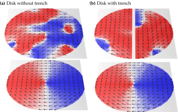
(a)Disk without trench (b)Disk with trench
Figure 3.2: Micromagnetic simulations results for the magnetisation. Field lines
are shown and colours denote up (red) or down (blue) direction. (a) Bottom: Magnetisation for a 45 nm disk of cobalt. Top: Magnetisation for a 1.5 nm disk of nickel parallel to the cobalt. (b)a trench is introduced in the nickel. Image taken from E. Beukers [35].
22 Lateral cobalt Junctions
Figure 3.3:Map of the magnetic inhomogeneity in a disk. The magnetic
inhomo-geneity is defined by the sine of the angle between the magnetisation in the two layers. The non-collinearity is highest around the trench in the middle. Image taken from E. Beukers [35].
In a 45 nm disk of cobalt, shown at the bottom of figure 3.2a and 3.2b, the disk is magnetised in a circular, vortex-like manner. This minimises the stray fields, as all the flux lines are contained within the magnet.
A 2nm layer of nickel on top is a much softer magnet and has a lower co-ercive field. The influence of the harder cobalt magnet on the softer nickel magnet is minimised as there are no stray fields. This decouples the two magnetic layers. This can be seen as the magnetisation of the nickel disk, shown at the top of figure 3.2a, is not fully aligned and shows random domains, independent of the magnetisation of the underlying cobalt.
Besides decoupling the two magnets, it is possible in this configuration to maximise the magnetic non-collinearity, by setting the magnetisation di-rection of the nickel along the junction. This junction is created by making an incision or trench in the top nickel layer, but leaving the cobalt disk in-tact, as shown in figure 3.2a. The magnetisation in the two nickel halves will now align along the junction, as this configuration minimises the stray
22
3.3 Magnetic inhomogeneity in a disk 23
fields. The mismatch in geometry between the full cobalt disk, where the field goes round, and the two nickel half disks, where the magnetisation is along the trench, causes the magnetisation directions of the two ferromag-nets two be perpendicular in the region around the trench. The magnetic inhomogeneity is defined by the sine of the angle between the magnetisa-tion in the two layers. A map of the magnetic inhomogeneity in figure 3.3 proves that the magnetic non-collinearity is maximised around the trench in this configuration.
Chapter
4
Nanofabrication
4.1
Design
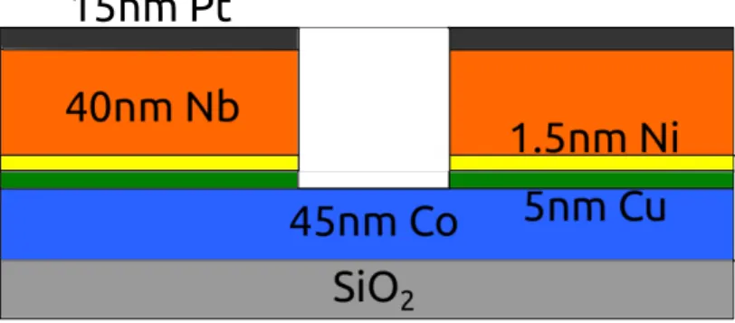
15nm Pt
Figure 4.1:Overview of the multilayer lateral junction.
To make a S/F/F’/F/S Josephson junction, as shown in figure 4.1, we em-ployed several nanofabrication techniques. A multilayer structure is to be patterned and sputtered onto a SiO2substrate. A 45 nm bottom layer of the ferromagnet cobalt (blue) is to be the weak link in the junction and bridg-ing the two niobium superconductors (orange) on top. A lateral junction is defined by having a current in the plane of the device. It is the current through the cobalt that defines this as a lateral junction.
26 Nanofabrication
(a)Disk with trench (b)Coarse structure and leads
Figure 4.2: (a)A SEM image of the finished disk and the junction. (b)The coarse
structure of the leads and in the middle the 5µm square that will be patterned
later. The independent structure in the bottom left corner is used for focussing.
completely cuts the Nb/Ni/Cu layers, but stops at the Co layer. The 15 nm platinum (grey) layer on top is to function as a hard mask for later patterning steps, with Focused Ion Beam (FIB) milling and Reactive Ion Etching (RIE). The platinum also acts as a capping layer to prevent the niobium from oxidising.
The full fabrication process will be described below, but a SEM image of the final disk structure can be seen in figure 4.2a. The structure consists of a 1µm sized disk, with a narrow<50 nm trench in the middle. On the
left and rights four superconducting leads can be seen, for a four-point measurement.
4.2
Design requirements
In order to create a proximised junction there are several requirements that we identified.
• Trench width
The length of any Josephson junction is limited by the Spin Diffusion Length (SDL) of the Cooper pairs in the weak link. The trench width has to be < 2×SDL ≈ 100 nm. However, we want to start on a
26
4.3 Fabrication steps 27
smaller gap and then increase it to determine the upper limit.
• High aspect ratio for trench
In order to have a well defined trench width a high etch anisotropy is desirable for the trench.
• Transparent interfaces
Interfaces between layers should be transparent. Mismatching of the Fermi energies at the interface increases resistance. This prevents the transmission of the triplet pairs.
• Limited defects and impurities
Triplet Cooper pairs can scatter at defects or impurities, decreasing the SDL and reducing the maximum trench width. The Tc of the
singlet niobium and triplet cobalt superconductivity will lower as a result of impurities.
4.3
Fabrication steps
4.3.1
Sputtering of multilayer structure
E-beam lithography was only used to pattern a coarse structure, contain-ing the contacts, leads and a 5µm square area to be patterned with the disk
shaped junction at a later step. Degassing of PMMA has an adverse effect on the superconductivity at the edges of the niobium. To mitigate this, all the leads were made ofµm sized structures and the disk shaped junction
is defined in a different step. The leads leading to the junction area are shown in the SEM image of figure 4.2b. The coarse structure and contact pads were defined with E-beam lithography at a dose of 360µC/cm2and
a positive photoresist (bilayer of 600K and 950K PMMA) on a SiO2 sub-strate.
After developing the PMMA, sputter deposition in a Ultra High Vacuum (UHV) chamber was used to deposit the multilayers of Nb(40 nm)/Ni(1.5 nm)/ Cu(5 nm)/Co(45 nm) at an argon pressure of 4E-3 mbar. The timings were determined to be 10’:04” at a current set point of 100 mA for Co, 28” at 65 mA for Cu, 29” at 100 mA for Ni and 12’:43” at 200 mA for Nb.
28 Nanofabrication
out of vacuum and immediately transferred to a different sputtering sys-tem, where 15 nm of platinum was deposited on top. This was done at an argon pressure of 5E-3 mbar at 1 kV.
The coarse structure was then created by means of lift-off with acetone. For this purpose the sample was soaked in acetone for 10 minutes, then put in a ultrasonic bath for two minutes with the acetone. Subsequently transferred to isopropanol and blow dried with nitrogen to prevent any dry marks.
4.3.2
Focused Ion Beam (FIB) milling
In order to create the high resolution, high aspect ratio trench for the junc-tion we settled on Focused Ion Beam (FIB) milling. Several other methods were attempted. Reactive Ion Etching (RIE) has the advantage of very high selectivity, with the ability to only etch the niobium layer. However, this comes at a reduced resolution and anisotropy. Argon etching of the Ni(1.5 nm)/Cu(5 nm) proved unsuitable due to increased side wall rede-position for the small trench width. Potentially, Helium Ion Microscope (HIM) milling offers improved performance over FIB, with less induced damage. Unfortunately, the HIM, that we could have access to, was out of commission and unavailable for this project. For future improvements it might still be a good replacement.
Focused Ion Beam (FIB) milling has several features that make it suitable for this project:
• High aspect ratio/anisotropy
FIB offers very high aspect ratio or mill anisotropy, this is suitable for creating narrow and deep trenches.
• Good resolution
Features with sizes down to 10 nm can be patterned with FIB.
The price to pay for this performance comes in the form of:
• Very little selectivity
Mill rates of Nb/Ni/Cu/Co are very similar.
• Control of depth proves difficult
The very small area of the trench only requires a minimal dose with FIB. The quality of focus of the ion beam has a large influence at this small resolution and dose. Combined with the lack of selectivity to
28
4.3 Fabrication steps 29
stop at a particular layer in the stack, the control of depth proves difficult.
• Induces local damage
FIB is locally quite destructive and induces a local damage. This can be problematic for the superconductivity around the junction. To mitigate this we employ a 15 nm platinum hard mask on top of the niobium. As platinum has a good stopping power for the secondary electrons involved in the milling process. This hard mask protects the superconducting niobium around the trench.
Figure 4.3: The coarsely structured square is patterned with FIB. An area is
re-moved to pattern the disk. Two incisions to the left and right are made to isolate the four contact leads. The trench is milled at the lowest possible current setting.
30 Nanofabrication
The final sample was then wirebonded to contacts of a sample holder and measured in a cryostat.
4.4
Verifying trench depth
Figure 4.4:For multiple devices on three different samples resistances are shown
as a variation with FIB mill time. Three different samples have potentially dif-ferent layer thicknesses, however the graph shows that even devices on the same sample have different resistances. There is a slight upward trend visible, but we do not believe that this is due to any difference in the resistance of the trench. The devices are each milled with FIB indiviually and their pattern and alignment are set manually, thus the geometry and resistance of each disk could be slightly different.
An important aspect of our fabrication process is that we need to create a trench that disconnects both sides of the junction leaving only a weak link
30
4.4 Verifying trench depth 31
through the underlying cobalt. For this we need to fully cut through the layers of Pt(15 nm)/Nb(40 nm)/Ni(1.5 nm)/Cu(5 nm). The FIB milling of this trench should preferably leave most of the cobalt underneath intact, as cutting into the cobalt has two effects. Firstly, it increases the distance the superconducting correlations have to travel. This effectively increases the trench width. Secondly, the more the cobalt is milled, the more damage is induced, hampering superconductivity.
The FIB mill depth and dose is controlled by the FIB milling time. By varying the time spent milling one spot, the milling depth can be chosen. In the FIB setup there is no possibility of directly measuring this depth. So the mill time needs to be determined and optimised by some other method.
The electrical resistance of the finished junction is made up of the resis-tance of the bulk layers of the junction plus the resisresis-tance of the weak link. Theoretically the resistance of the weak link should increase slightly as the trench becomes deeper.
We measured the resistance of several devices as a function of FIB milling time. This was done by a four-point measurement in a probe station. The resulting graph of three samples with devices milled for different dura-tions is figure 4.4.
(a)Full multilayer structure
15nm Pt
(b)Control Sample without cobalt
40nm Nb
SiO2 15nm Pt
1.5nm Ni
5nm Cu
Figure 4.5:Control samples were made without the bottom cobalt layer.
A simplified calculation of the resistances for a layer of metal in the vol-ume of the trenchR = ρAl for a 1µm long and 50 nm wide trench, can give
32 Nanofabrication
FIB mill time BL200856 BL01102 seconds resistanceΩ resistanceΩ
0.3 - 15.6
0.3 - 16.6
0.5 12.56 17.6
0.5 - 17.6
0.8 Infinite 20.61
1.0 16.4 26.91
1.0 Infinite Infinite
1.2 Infinite 18.4
1.5 Infinite
-Table 4.1: The resistances for two control samples without cobalt were
deter-mined with a four point measurement. Each sample contains devices that have been milled with FIB for different times. Dashes - denote that there is no corre-sponding device for that FIB time. When the sample is cut all the way through, there is no electrical connection and the resistance is infinite.
The resistance of the disk structure is thus higher than that of the weak link, due to the trench. Looking at the variations in resistance for the sam-ples with FIB time, we must conclude that the variations actually come from differences in the disk geometry, which is not unlikely as all the in-cisions and alignments are done by hand and the devices are not exact replicas. Looking at resistance of the full multilayer structure is thus not very enlightening.
For this purpose we made control samples that have the bottom layer of cobalt omitted as shown in figure 4.5b. When we fabricate the trench now, the weak link consists of insulating SiO2. Thus for a fully milled trench, electrical contact is expected to be broken and the resistance should shoot up.
Measured resistances of disks without Cobalt are in the range of 17-25 Ω for the cases where there is still electrical contact and infinite for the purpose of measuring them when they have been cut through.
For several devices on two control samples the resistances are shown in table 4.1. At FIB times below 0.5 s all devices are still connected. The first device shows an infinite resistance at 0.8 s. Unfortunately there is no strong cut off point in FIB time, where the control samples become insulating. As even for longer FIB times of 1.2 s some devices are still conducting. Milling longer would affect the cobalt too much.
32
4.4 Verifying trench depth 33
The trench depth is strongly affected by the quality of the focus. The vari-ation in focussing affects the dose per area. For the very low doses that we are trying to achieve, focussing is dominant in determining the dose. This makes the FIB milling time an unsuitable parameter to determine the trench depth. We have therefore settled on FIB times of longer than one second, as most control devices show infinite resistance at those times, and simply hope that we create a fully cut junction.
Chapter
5
Results
5.1
Superconducting samples
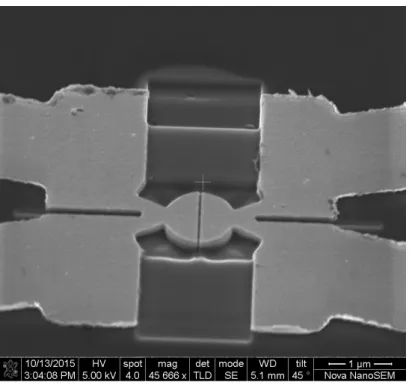
We succeeded in making devices with trench widths below 20nm. Device A as seen in figure 5.1a has an approximate junction width of 25nm, while device B, seen in figure 5.1b, has an even sharper trench of about 17nm.
(a)Device A (b)Device B
Figure 5.1:Two devices on the same substrate, but with different junction length.
36 Results
The SEM images show the contrast between the metallic multilayer struc-ture lighter on top and the exposed insulating SiO2 that is darker. This tells us that the disk is formed correctly. The two trenches are seen in the middle of the disk, although for device B the trench is slightly off centre, a result of the manual alignment in the FIB.
The trench cut can also be seen to continue into the SiO2, at the edges. This is a result of the FIB milling rate being faster at the edge of the structure. This does not imply that the trench has also cut into the SiO2in the middle of the disk. The side view of the trench does seem to indicate that the incision is quite deep and likely to have cut through most of the layers and possibly some distance into the cobalt. This is an indication that the trench is well formed.
Figure 5.2:Device A and B both show a first transition around 5.5 K,
correspond-ing to the niobium in the leads and disk gocorrespond-ing superconductcorrespond-ing. The resistance of device A remains constant at 250 mΩup to 2.0 K, while the resistance of device B starts to approach zero from 2.8 K. This indicates that device B is experiencing a second transition.
The RT-curve obtained by cooling the sample down in a cryostat can be seen in figure 5.2. Going below 6 Kelvin shows a rapid transition in the
36
5.1 Superconducting samples 37
resistance of the devices. The resistance rapidly decreases from 3.5Ωand 2.5 Ω to about 250mΩ. This indicates that the niobium in the leads and disk is going superconducting.
At lower temperature the resistance of device A (in blue) remains quite constant at 250mΩ all the way up to 2.0 Kelvin. Device B (in red) on the other hand starts to gradually decrease in resistance from about 2.8K and below. The resistance starts to approach 0 at 2.0K.
Figure 5.3: The IV-curves go from straight normal resistance at 2.8 K to curved
with a critical current at 2.0K. The slope does not reach zero for 2.0 K.
Individual IV curves in figure 5.3 taken at different temperatures between 2.8 K and 2 K show that the decrease in resistance for device B is really a superconducting transition with a critical current above which the resis-tance will return to its normal value. The resisresis-tance around zero current does remain finite at about 10 mΩ, but shows a strong downward trend suggesting that it will go to zero below 2 K.
temper-38 Results
ature of device B seems to be around this temperature, it leaves open some question. While we have strong indications that the resistance would go to zero at lower temperatures, it would have been nice to actually see it. Furthermore it is possible that device A would also start approaching zero resistance for temperatures below 2K, although the resistance is constant at 250 mΩand there is no downward trend.
Figure 5.4: IV curves are shifted vertically with the field. The scale from yellow
to blue indicates the measuered voltage for the applied current. The transistion from yellow to blue is choosen by eye to highlight the critical current.
Normally the critical current Ic of a superconductor decreases as an
exter-nal field is applied and will disappear completely above some critical field Hc. This is not the case for device B. Sweeping the applied out-of-plane
field from 60 mT to -60 mT, reveals an oscillating critical current. This is visualised in figure 5.4 for the range of -40 mT to 10 mT. Here individual IV curves are shifted above each other with respect to the field value they were taken in. The colour scale from yellow to blue shows the measured voltage with respect to the applied current. The transition from yellow to blue is set to highlight the critical current.
The pattern in figure 5.4 is clearly oscillating with the applied field. Within the yellow parts of the graph, the resistance is close to zero and the graph nearly flat. In the blue parts the slope is constant and equal to the normal
38
5.2 Critical current 39
resistance of the junction.
5.2
Critical current
Looking at where this transition occurs allows us to track what the critical current is doing. We analysed the critical current by looking at each indi-vidual IV-curve and selecting the data point for which the curve started to deviate from the linear normal regime. We did this for both negative and positive current and used the average value. We are aware that this point does not match the usual definition of critical current. Choosing this point allows us to analyse the behaviour of the resistance in a relatively consis-tent manner even when the junction does not go fully superconducting and a finite resistance or slope remains.
Picking the point for the critical current in this manner, allows us to con-sistently determine the current within 1µA. The resulting graph of critical
current against field is seen in figure 5.5.
The graph clearly shows the critical current varying and disappearing completely at fields above 60 mT. The oscillations are occurring quite rapidly at this field scale. We will focus our analysis on fields from -30 mT to 30 mT as shown in figure 5.6.
The critical current around zero field is varies 10-20 µA. With increasing
field strength, most notably the regions between 5 mT and 15 mT, -5 mT and -15 mT, the critical current reaches values as high as 36µA and is
over-all much higher. This is very unusual for singlet superconductivity and is a strong indicator that this is triplet superconductivity where magnetic in-homogeneity is important. As the field is increased the magnetisation of the thin nickel layer is turning out-of-plane. The cobalt layer has a much higher out-of-plane magnetic coercivity and remains in-plane[38]. This increases the magnetic non-collinearity between the Co and Ni, which in-troduces more triplet correlations into the cobalt and could thus be respon-sible for the increased critical current.
40 Results
Figure 5.5: Critical current as determined by looking at the point where the
IV-curve start to deviate from linear. For field strengths above 60 mT and -60 mT the IV-curves are fully linear. The high fields for which there was no critical current effect are not shown in this figure.
same field while then yield a different critical current. The junction really seems undergo a transition to a different state. This could be caused by individual magnetic domains in the nickel reversing direction.
Repeated magnetic field sweep measurements on the sample show the same behaviour. While the exact values of the critical current and the peak positions differ, the general trend is always present. The slightly chang-ing behaviour of the curve suggests that the behaviour of the junction is dependant on a changing configuration. The only configuration that can readily change is the magnetisation of the layers.
40
5.3 Resistance 41
Figure 5.6: Critical current as determined by looking at the point where the
IV-curve start to deviate from linear. For the fields between 30 mT and -30 mT. Oscillations are present with an approximate period of 4 mT. The arrows indicate the presence of sudden jumps in the critical current.
5.3
Resistance
42 Results
Figure 5.7:IV measurements are shifted vertically with applied field. The slope of
the IV curves around zero current changes. At 3.75 mT the sleep is much steeper than at 10 mT.
By determining the slope between -5 µA and 5 µA the resistance of the
junction around zero current is found. Figure 5.8 shows the change in resistance with field. The graph is much smoother now, as the resistance is close to zero for most fields, but really shoots up for some fields. These peaks correspond to the minima in the critical current of figure 5.6. A discussion of these oscillations while now follow.
42
5.3 Resistance 43
Figure 5.8: The resistance is determined by the slope between -5 µA and 5 µA.
Chapter
6
Discussion
6.1
Oscillations
There are several mechanisms that could give rise to oscillations with the magnetic field in the superconductivity. Most involve flux quantisation in some manner, with a period of the magnetic quantum flux:
Φ0 = h
2e. (6.1)
In a Josephson junction the magnetic field modulates the superconducting phase and this gives rise to a suppression of the critical current when there is an integral number of flux quanta in the junction. The dependence of the critical current on the magnetic flux is given by:
Ic = Ic0
sin(πΦ/Φ0) πΦ/Φ0
. (6.2)
Here the flux through the junction with area A is given by Φ = B·A. This pattern with periodΦ0is known as the Fraunhofer diffraction pattern [39, 40]. For our junction with dimensions of 1µm length and 20 nm width,
this would give us an oscillation with applied magnetic field at a period of about a 100 mT.
46 Discussion
Figure 6.1: The oscillations in the resistance of the junction for -40 mT to 0 mT.
The graph resembles that for flux quantisation in a loop.
Taking a closer look at the results for the resistance at negative fields in fig-ure 6.1, the pattern that is present in this graph is reminiscent of a different flux quantisation phenomenon, known as the Little-Parks effect [41]. The Little-Parks effect causes magnetoresistance oscillations right at the resis-tive transition, which coincides with where the measurements of device B were taken.
The flux through a thin superconducting ring can only take on integer val-ues due to flux quantisation. As a result, when the applied flux is not an integer of the flux quantum, a current will flow through the superconduct-ing rsuperconduct-ing to brsuperconduct-ing the flux up or down to an integer value.
While there is no thin ring in our case, we can calculate the required diam-eter to obtain a Little-Parks oscillation with the observed period between 3-4 mT. We find that this would correspond to a ring with a diameter of 800-940 nm. Our actual disk structure has a diameter of 1000 nm.
This strongly suggest that there is a link between the flux through our
46
6.2 Cobalt disk 47
disk and the observed fluctuations. While the Little-Parks effect is usually described in terms of a thin disk, with a homogeneous order parameter, there are some efforts to extend this effect to thick disks with an inhomo-geneous order parameter [42, 43]. These efforts show that there is a dimen-sional crossover from a 1D ring to a 2D disk with a hole. This dimendimen-sional crossover results in the parabolic background of the Little-Parks effect to become linear for disks with small holes.
The critical field of our junction is at 60 mT, which is insufficient to say anything conclusive on the behaviour of the background. While it is im-possible to say whether there is a linear or parabolic increase. There does seem to be a steady increase in the range from -10mT to -40mT.
6.2
Cobalt disk
It is important to realise that the only intact disk in our structure is the layer of cobalt at the bottom. The singlet superconductor niobium has been cut in half. We know that this is the case, because we fabricated another device indicated ML25092 which was only milled for 0.1 seconds using FIB. Its trench is much shallower as can be seen in the SEM image of figure 6.2b. This in contrast to figure 6.2a which shows the deep trench milled for 1s of device B.
ML25092 also experiences two superconducting transitions. The critical current for each transition is shown in figure 6.3a. The first transition cor-responds to the leads going superconducting at a temperature of 6.4 K. Directly followed by a second transition at 6.3 K. The critical temperature for the second transition of device B is below 2.8 K and reaches a maxi-mum critical current of 37 µA. The critical current achieved in ML25092
reaches almost 700 µA at a temperature of 4.0 K. In this sample the
nio-bium hasn’t been completely cut through and the second transition is that of the niobium disk going superconducting.
This contrasts strongly with the behaviour of device B, which is not fully superconducting even at 2K. Thus in device B we have cut through the niobium and it really is the cobalt layer that is the only intact disk.
48 Discussion
(a)Device B (b)ML25092
Figure 6.2: The trench in device B is milled with FIB for 1.0 second, as a result
it is much sharper and deeper than the trench in ML25092, which has only been milled for 0.1 second.
6.3
Triplet superconductivity
We have treated our devices mostly as a junction, but superconductiv-ity is really a macroscopic quantum phenomenon. It is therefore not en-tirely strange that the superconductivity of the entire disk influences the behaviour of the junction.
Magnetic inhomogeneity is essential for introducing superconducting triplet correlations into the cobalt disk. By applying a magnetic field the mag-netisation of the nickel layer is lifted out of plane and this increases the magnetic non-collinearity between the nickel layer and the cobalt, which has a very high out of plane magnetic coercivity. As the non-collinearity increases, more triplets correlations will be introduced to the cobalt.
The decrease in resistance observed in figure 6.1 from 0 to -10 mT could be due to an increase in magnetic inhomogeneity. At higher fields the increase in magnetic inhomogeneity loses from the suppression of the su-perconductivity due to the exchange field.
The observation of a flux quantisation effect in a solid disk, could be ex-plained by the particular magnetic inhomogeneity of this disk geometry. The magnetisation of cobalt goes round the disk and as a result the mag-netisation is low at the centre of the disk. The magnetic inhomogeneity
48
6.3 Triplet superconductivity 49
(a)ML25092 (b)Magnetic inhomogeneity of a disk
Figure 6.3: (a)The critical current determined for each transition. The first
tran-sition corresponds to the leads going superconducting and the second trantran-sition to the disk itself following shortly after. This shows that the niobium is not cut through. (b) The map of the magnetic inhomogeneity between the nickel and cobalt layers. This is the same graph as 3.3.
between Co and Ni at the centre of the disk is therefore also low. This can be seen in the simulation of the magnetic inhomogeneity in the repeated figure 6.3b. The blue region in the middle shows there is low magnetic in-homogeneity. Due to cobalt’s strong coercivity to out of plane fields, this does not change much at higher fields.
Chapter
7
Conclusion and outlook
We created a lateral proximised S/F/F’/F/S Josephson junction. With Focused Ion Beam (FIB) milling we succeeded in making devices with a trench width below 20 nm. The junction shows two transitions. The first transition occurs at a temperature of 5.5 K. The resistance changes from a normal resistance of 2.5 Ωto 250 mΩ and corresponds to the niobium in the structure going superconducting. The second transition occurs below 2.8 K and shows a steadily decreasing resistance approaching zero.
The weak link in the junction is formed by the cobalt disk at the bottom of the structure. We established that the trench has cut through all of the niobium. As a result of the ferromagnet in the weak link only supercon-ducting triplet correlations can proximise the junction.
There is an overall increase in the critical current for ranges between -15 mT and 15 mT with an applied out-of-plane magnetic field. The exchange field can orient the magnetisation of the nickel layer out-of-plane. This increases the magnetic non-collinearity between nickel and cobalt, lead-ing to an increase in the induced triplet correlations. This could be the mechanism behind the observed increase in critical current.
52 Conclusion and outlook
The cobalt disk has a circular magnetisation, with low magnetisation in the centre. This results in low magnetic inhomogeneity between the Co and the Ni at the middle. Limiting the amount of induced triplet corre-lations there. It is possible that the centre of the disk does not go fully superconducting as a result, while the surrounding ring does. It could be that it is this superconducting ring in the cobalt disk that is responsible for the flux quantisation effect.
Measurements below 2 Kelvin could provide more insights as currently the junction is right at the transition temperature. Additional evidence for triplet superconductivity could be obtained by measuring control samples without nickel. These samples should show a significantly reduced criti-cal current, as they lack the required magnetic inhomogeneity for triplet generation.
In general these results show the possibility of triplet superconductivity in a lateral cobalt Josephson junction.
52
References
[1] T. S. Khaire, M. A. Khasawneh, W. Pratt Jr, and N. O. Birge, Obser-vation of spin-triplet superconductivity in Co-based Josephson junctions, Physical review letters104, 137002 (2010).
[2] J. Robinson, J. Witt, and M. Blamire, Controlled injection of spin-triplet supercurrents into a strong ferromagnet, Science329, 59 (2010).
[3] R. Keizer, S. Goennenwein, T. Klapwijk, G. Miao, G. Xiao, and A. Gupta,A spin triplet supercurrent through the half-metallic ferromagnet CrO2, Nature439, 825 (2006).
[4] M. Anwar, F. Czeschka, M. Hesselberth, M. Porcu, and J. Aarts, Long-range supercurrents through half-metallic ferromagnetic CrO 2, Physical Review B82, 100501 (2010).
[5] H. K. Onnes,The superconductivity of mercury, Comm. Phys. Lab. Univ. Leiden122, 124 (1911).
[6] J. Bardeen, L. N. Cooper, and J. R. Schrieffer,Theory of superconductiv-ity, Physical Review108, 1175 (1957).
[7] J. G. Bednorz and K. A. M ¨uller,Possible high T c superconductivity in the Ba—La—Cu—O system, inTen Years of Superconductivity: 1980–1990, pages 267–271, Springer, 1986.
[8] M. Eschrig,Spin-polarized supercurrents for spintronics, Phys. Today64, 43 (2011).
54 References
The Physics of Organic Superconductors and Conductors, pages 687–704, Springer, 2008.
[10] A. Larkin and Y. N. Ovchinnikov, Neodnorodnoe sostoyanie sverkh-provodnikov, Zh. Eksp. Teor. Fiz47, 1136 (1964).
[11] P. Fulde and R. A. Ferrell, Superconductivity in a strong spin-exchange field, Physical Review135, A550 (1964).
[12] V. Berezinskii,New model of the anisotropic phase of superfluid He3, Jetp Lett20, 287 (1974).
[13] P. Coleman, E. Miranda, and A. Tsvelik, Odd-frequency pairing in the Kondo lattice, Physical Review B49, 8955 (1994).
[14] E. Abrahams, A. Balatsky, D. Scalapino, and J. Schrieffer,Properties of odd-gap superconductors, Physical Review B52, 1271 (1995).
[15] J. Linder and J. W. Robinson, Superconducting spintronics, Nature Physics11, 307 (2015).
[16] F. Bergeret, A. Volkov, and K. Efetov, Long-range proximity effects in superconductor-ferromagnet structures, Physical review letters86, 4096 (2001).
[17] H. Meissner,Superconductivity of contacts with interposed barriers, Phys-ical Review117, 672 (1960).
[18] A. Andreev, Thermal conductivity of the intermediate state of supercon-ductors, Zh. Eksperim. i Teor. Fiz.46(1964).
[19] G. Blonder, M. Tinkham, and T. Klapwijk, Transition from metallic to tunneling regimes in superconducting microconstrictions: Excess current, charge imbalance, and supercurrent conversion, Physical Review B 25, 4515 (1982).
[20] I. Karonen, https://en.wikipedia.org/wiki/File:Andreev_ reflection.svg, public domain.
[21] A. I. Buzdin,Proximity effects in superconductor-ferromagnet heterostruc-tures, Reviews of modern physics77, 935 (2005).
[22] A. Volkov, F. Bergeret, and K. B. Efetov, Odd triplet superconductivity in superconductor-ferromagnet multilayered structures, Physical review letters90, 117006 (2003).
54
References 55
[23] F. Bergeret, A. Volkov, and K. Efetov,Odd triplet superconductivity and related phenomena in superconductor-ferromagnet structures, Reviews of modern physics77, 1321 (2005).
[24] M. Houzet and A. I. Buzdin,Long range triplet Josephson effect through a ferromagnetic trilayer, Physical Review B76, 060504 (2007).
[25] S. Parkin, N. More, and K. Roche,Oscillations in exchange coupling and magnetoresistance in metallic superlattice structures: Co/Ru, Co/Cr, and Fe/Cr, Physical Review Letters64, 2304 (1990).
[26] M. Anwar, M. Veldhorst, A. Brinkman, and J. Aarts, Long range su-percurrents in ferromagnetic CrO2 using a multilayer contact structure, Applied physics letters100, 052602 (2012).
[27] J. Linder, Y. Tanaka, T. Yokoyama, A. Sudbø, and N. Nagaosa, Inter-play between superconductivity and ferromagnetism on a topological insu-lator, Physical Review B81, 184525 (2010).
[28] B. D. Josephson, Possible new effects in superconductive tunnelling, Physics letters1, 251 (1962).
[29] B. F. Field, The calibration of dc voltage standards at NIST, Journal of Research of the National Institute of Standards and Technology 95, 237 (1990).
[30] D. Van Harlingen, Phase-sensitive tests of the symmetry of the pairing state in the high-temperature superconductors—evidence for d x 2- y 2 sym-metry, Reviews of Modern Physics67, 515 (1995).
[31] V. Ryazanov, V. Oboznov, A. Y. Rusanov, A. Veretennikov, A. Golubov, and J. Aarts,Coupling of two superconductors through a ferromagnet: evi-dence for aπ junction, Physical review letters86, 2427 (2001).
[32] T. Kontos, M. Aprili, J. Lesueur, F. Genet, B. Stephanidis, and R. Bour-sier,Josephson junction through a thin ferromagnetic layer: negative cou-pling, Physical review letters89, 137007 (2002).
[33] M. Anwar and J. Aarts, Inducing supercurrents in thin films of ferro-magnetic CrO2, Superconductor Science and Technology 24, 024016 (2011).
56 References
[35] E. Beukers, Spin-polarized superconductivity in superconductor-ferromagnet hybrids: simulations and experiment, Master’s thesis, Leiden University, 2015.
[36] M. J. Donahue and D. G. Porter, OOMMF User’s guide, US Depart-ment of Commerce, Technology Administration, National Institute of Standards and Technology, 1999.
[37] J. M. Coey, Magnetism and magnetic materials, Cambridge University Press, 2010.
[38] W. Sterk, Magnetisation characteristics of noncollinear ferromagnetic bi-layers, Master’s thesis, Leiden University, 2015.
[39] J. Heida, B. Van Wees, T. Klapwijk, and G. Borghs,Nonlocal supercur-rent in mesoscopic Josephson junctions, Physical Review B 57, R5618 (1998).
[40] J. Rowell,Magnetic field dependence of the Josephson tunnel current, Phys-ical Review Letters11, 200 (1963).
[41] W. Little and R. Parks,Observation of quantum periodicity in the transi-tion temperature of a superconducting cylinder, Physical Review Letters
9, 9 (1962).
[42] V. Bruyndoncx, L. Van Look, M. Verschuere, and V. Moshchalkov, Di-mensional crossover in a mesoscopic superconducting loop of finite width, Physical Review B60, 10468 (1999).
[43] M. Morelle, D. S. Golubovi´c, and V. V. Moshchalkov,Nucleation of su-perconductivity in a mesoscopic loop of varying width, Physical Review B
70, 144528 (2004).
56