Qucs
A Tutorial
Getting Started with Qucs
Stefan Jahn
Juan Carlos Borr´
as
Copyright c 2007 Stefan Jahn <[email protected]>
Copyright c 2007 Juan Carlos Borr´as<[email protected]>
Permission is granted to copy, distribute and/or modify this document under the terms of the GNU Free Documentation License, Version 1.1 or any later version published by the Free Software Foundation. A copy of the license is included in the section entitled ”GNU Free Documentation License”.
Introduction
The following sections are meant to give an overview about what the Qucs software can be used for and how it is used to achieve this.
Qucs is free software licensed under the General Public License (GPL). It can be downloaded from http://qucs.sourceforge.net and comes with the complete source code. Every user of the program is allowed and called upon (on a voluntary basis of course) to modify it for their purposes as long as changes are made public. Contact the authors to verify them and finally to incorporate it into the software. The software is available for a variety of operating systems including
• GNU/Linux • Windows • FreeBSD • MacOS • NetBSD • Solaris
On the homepage you’ll find the source code to build and install the software. Build instructions are given. Also links for binary packages for certain distributions (e.g. Debian, SuSE, Fedora) can be found.
Once the software has been successfully installed on your system you can start it by issuing the
# qucs
command or by clicking the appropriate icon on your start menu or desktop. Qucs is a multi-lingual program. So depending on your system’s language settings the Qucs graphical user interface (GUI) appears in different languages.
Figure 1: Qucs has been started
On the left hand side you find the Projects folder opened. Usually the projects folder will be empty if you use Qucs for the first time. The large area on the right hand side is the schematic area. Above you can find the menu bar and the toolbars.
In the File → Application Settings menu the user can configure the language and appearance of Qucs.
Figure 2: Application setting dialog
To take effect of the language and font settings the application must be closed either via the Ctrl + Q shortcut or the File → Exit menu entry. Then start Qucs again.
Tool suite
Qucs consists of several standalone programs interacting with each other through the GUI. There are
• the GUI itself,
The GUI is used to create schematics, setup simulations, display simulation results, writing VHDL code, etc.
• the backend analogue simulator,
The analogue simulator is a command line program which is run by the GUI in order to simulate the schematic which you previously setup. It takes a netlist, checks it for errors, performs the required simulation actions and finally produces a dataset.
• a simple text editor,
The text editor is used to display netlists and simulation logging informa-tions, also to edit files included by certain components (e.g. SPICE netlists, or Touchstone files).
• a filter synthesis application,
• a transmission line calculator,
The transmission line calculator can be used to design and analyze different types of transmission lines (e.g. microstrips, coaxial cables).
• a component library,
The component library manager holds models for real life devices (e.g. tran-sistors, diodes, bridges, opamps). It can be extended by the user.
• an attenuator synthesis application,
The program can be used to design various types of passive attenuators.
• a command line conversion program
The conversion tool is used by the GUI to import and export datasets, netlists and schematics from and to other CAD/EDA software. The supported file formats as well as usage information can be found on the manpage of quc-sconv.
Additionally the GUI steers other EDA tools. For digital simulations (via VHDL) the program FreeHDL (see http://www.freehdl.seul.org) is used. And for circuit optimizations ASCO (see http://asco.sourceforge.net) is configured and run.
Setting up schematics
The following sections will enable the user to setup some simple schematics. For this we first create a new project named “WorkBook”. Either press the New
button above the projects folder or use the menu entryProject→New Project
and enter the new project name.
Figure 3: New project dialog
Confirm the dialog by pressing the “Create” button. When done, the project is opened and Qucs switches to theContent tab.
Figure 4: New empty project has been created
In the Content tab you will find all data related to the project. It contains your schematics, the VHDL files, data display pages, datasets as well as any other data (e.g. datasheets). On the right hand side an “untitled” and empty schematic window is displayed.
Now you can start to edit the schematic. The available components can be found in the Components tab.
Figure 5: Components tab
In fig. 5 is shown when clicking the Components tab. There are lumped com-ponents (e.g. resistors, capacitors), sources (e.g. DC and AC sources), transmis-sion lines (e.g. microstrip, coaxial cable, twisted pair), nonlinear components (e.g. ideal opamp, transistors), digital components (e.g. flip-flops), file components (e.g. Touchstone files, SPICE files), simulations (e.g. AC or DC analysis), diagrams (e.g. cartesian or polar plot) and paintings (e.g. texts, arrows, circles).
Each of the components can placed on the schematic by clicking it once, then move the mouse cursor onto the schematic and click again to put it on its final position. During the mouse move you can right click in order to rotate the component into its final position. The user can also drag-and-drop the components.
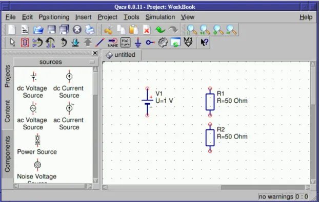
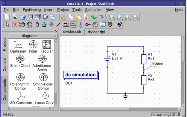
DC simulation - A voltage divider
The DC analysis is a steady state analysis. It computes the node voltage as well as branch currents of the complete circuit. The given circuit in fig. 6 is going to divide the voltage of a DC voltage source according to the resistor ratio.
Figure 6: Components of the voltage divider place in the schematic area
Wiring components
Now you need to connect the components appropriately. This is done using the wiring tool. You enable the wiring mode either by clicking the wire icon or by pressing the Ctrl + E shortcut. Left clicking on the components’ ports (small red circles) starts a wire, clicking on a second port finishes the wire. In order to change the orientation of the wire right click it. You can leave the wiring mode by the pressing Esc key.
Figure 7: Components of the voltage divider appropriately wired
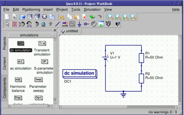
For any analogue simulation (including the DC simulation) there is a reference potential required (for the nodal analysis). The ground symbol can be found in the Components tab in thelumped components category. The user can also choose the ground symbol icon or simply press the Ctrl + G shortcut. In the given circuit in fig. 8 the ground symbol is placed at the negative terminal of the DC voltage source.
Placing simulation blocks
The type of simulation which is performed must also be placed on the schematic. You choose the “DC simulation” block which can be found in the Components
Figure 8: Ground symbol as well as DC simulation in place
Labelling wires
If you want the voltage between the two resistors (the divided voltage) be output in the dataset after simulation the user need to label the wire. This is done by double clicking the wire and given an appropriate name. Wire labelling can also be issued using the icon in the toolbar, by pressing the Ctrl + L shortcut or by choosing theInsert → Wire Label menu entry.
Figure 9: Node label dialog
The dialog is ended by pressing the Enter key of pressing the “Ok” button. Now the complete schematic for the voltage divider is ready and can be saved. This can by achieved by choosing theFile →Savemenu entry, clicking the single disk icon or by pressing the Ctrl + S shortcut.
Figure 10: File save dialog
The final DC voltage divider is shown in fig. 11.
Issuing a simulation
The schematic can now be simulated. This is started by choosing theSimulation
→ Simulate menu entry, clicking the simulation button (the gearwheel) or by pressing the F2 shortcut.
Figure 12: Empty data display after simulation finished
After the simulation has been finished the related data display is shown (see fig.12). Also the Components tab has changed its category to “diagrams”.
Placing diagrams
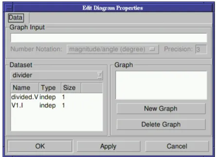
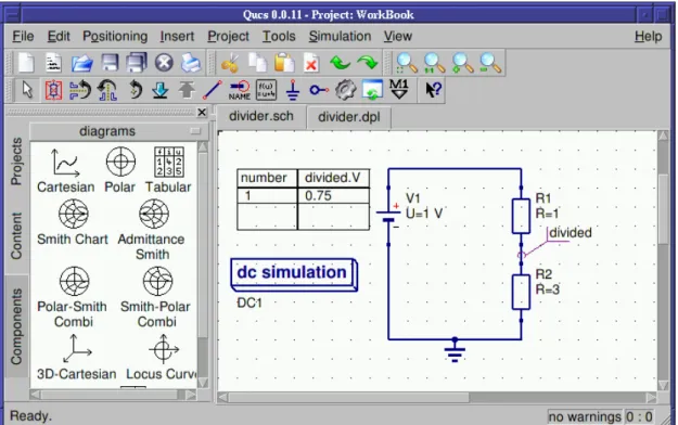
Choose the tabular (list of values) diagram and place it on the data display page. After dropping the tabular, the diagram dialog appears as shown in fig. 13.
Figure 13: Diagram dialog
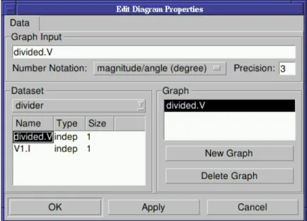
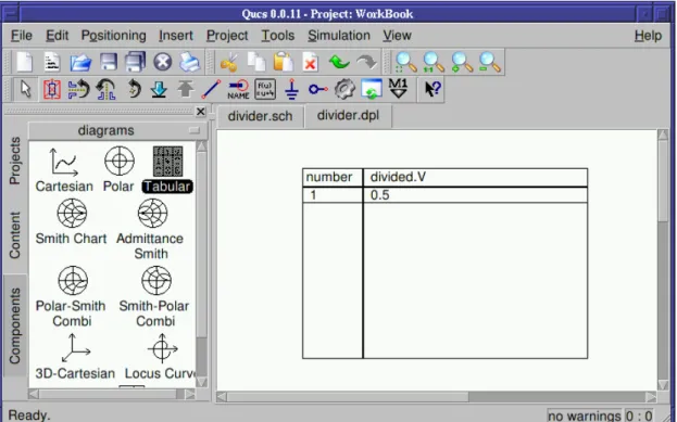
By double clicking thedivided.Vthe graph (i.e. values in a tabular plot) is added to the diagram. Beside the node voltage divided.V also the current through the DC voltage source V1.I is available. Only items listed in the dataset list can be put into the graph.
Available dataset items
Depending on the type of simulation the user performed you find the following types of items in the dataset.
• node.V – DC voltage at node node
• name.I– DC current through component name
• node.v– AC voltage at node node
• name.i– AC current through component name
• node.vn– AC noise voltage at node node
• name.in – AC noise current through componentname
• node.Vt – transient voltage at nodenode
• S[1,1] – S-parameter value
Please note that all voltages and currents are peak values and all noise voltages are RMS values at 1Hz bandwidth.
Figure 14: Diagram dialog with the node voltage added
Depending on the type of graph you have various options to choose for the graph. For a tabular graph there is the the number precision as well as type of number notation (important for complex values). Press the “Ok” button to close the dialog.
Figure 15: Data display with tabular graph
In the tabular graph you see now the value of the node voltage divided.V which is 0.5V. That was expected since the values of the resistors are equally sized and the DC voltage source produces 1V.
Congratulations! You made your first successful simulation using Qucs.
Changing component properties
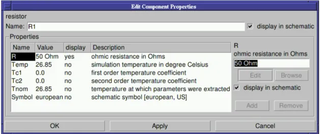
If you want to change the resistor ratio then switch back to your schematic either by clicking on thedivider.sch tab, by pressing the F4 shortcut or by choosing the Simulation → View Data Display/Schematic menu entry. Afterwards double click theR1 resistor. This opens the component property dialog shown in fig. 16.
Figure 16: Component property dialog for the R1 resistor
In the component property dialog all the properties of a given component can be edited. A short description is given as well as there is a checkbox for each property
display in schematic which can be used to add the property name and value on the schematic (or to hide it).
Allowed property values For component values either standard (1000), scien-tific (1e-3) or an engineering (1k) number notation can be chosen. Some units are also allowed. The units are
• Ohm – resistance / Ω • s – time / Seconds • S – conductance / Siemens • K – temperature / Kelvin • H – inductance / Henry • F – capacitance / Farad • Hz – frequency / Hertz • V – voltage / Volt • A – current / Ampere • W – power / Watt
• m – length / Meter (not usable standalone, see paragraph below) The available engineering suffixes are
• dBm – 10· log (x/0.001) • dB – 10· log (x) • T – 1012 • G – 109 • M – 106 • k – 103 • m – 10−3 • u – 10−6 • n – 10−9 • p – 10−12 • f – 10−15 • a – 10−18
Please note that all units and engineering suffixes arecase sensitiveand also note the conflict in m. When specifying one millimeter you can use 1mm. One meter (1m) cannot be specified and will always be interpreted as one milli (engineering notation).
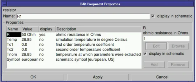
Figure 17: Component property dialog for the R1 resistor
Figure 18: Value of resistor R1 changed
In order to change the value of the resistor R2you can just click on the 50 Ohm
value directly on the schematic and edit the value.
Figure 19: Change value of resistorR2 directly on schematic
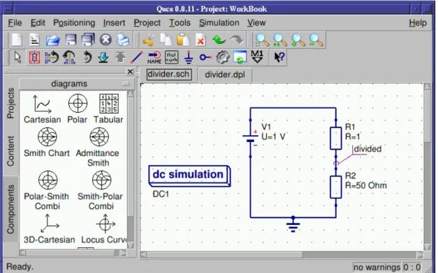
Change the value to “3” which will give a resistor ratio of 3/(1 + 3) = 0.75. Now you have the following schematic.
Figure 20: Value of resistor R2 changed
Diagrams are not limited to be placed on the data display, they can also reside on the schematic directly. Thus you can place again now a tabular diagram on the schematic and add the divided.V value. The diagram will show the result from the previous simulation.
Changing document properties
If you do not want Qucs to change automatically to the associated data display you can change the behaviour in the document setting dialog. You can go to the document settings dialog by right clicking on free space on the schematic area and choose the Document Settings menu item in the context menu which pops up or by choosing the File → Document Settings menu entry.
Figure 21: Document settings dialog
In the dialog you uncheck theopen data display after simulation item. Press the “OK” button to apply the change. If you now resimulate the schematic by pressing the F2 shortcut the “Qucs Simulation Messages” dialog window opens and can be left by pressing Esc . The tabular diagram now show the new value for divided.V.
Figure 22: Divider schematic after new simulation
DC simulation - Characteristics of a transistor
We are now going ahead and will setup schematics for some characteristic curves of a bipolar transistor using DC simulation and the parameter sweep.
I 1 I = Ib V 1 U = 10 arame t er s weep S W1 S i m = D C 1 T ype = l og P aram = Ib S t ar t = 10 n S t op = 10 m P o i n t s = 101 d c s i mu l a t i on DC1 Q 2N4401 _ 1
Figure 23: Swept DC simulation setup
In the schematic in fig. 23 there is a bipolar transistor placed in a common emitter configuration. Additionally a parameter sweep has been placed. Please note the
Sim property of the parameter sweep. It contains the instance name of the DC simulation DC1 which is going to be swept. The parameter which is swept is Ib
(the base current) and is put into the Param property of the parameter sweep. The parameter Ibis also put into the Iproperty of the DC current source I1.
Using the component library
The bipolar transistor has been taken from the component library. You can start the program by choosing the Tools → Component Library menu entry or by pressing the Ctrl + 4 shortcut.
Figure 24: Component library tool
When choosing the “Transistor” category with the combobox you find the “2N4401” transistor. By clicking the “Copy to clipboard” button the component is available in the clipboard and can be inserted in the schematic using the Ctrl + V shortcut or by choosing theEdit→Pastemenu entry. The component can also by dragged onto the schematic by clicking on the symbol in the library tool.
So what do we want to simulate actually? It is the current transfer curve of the bipolar transistor. The input current (at the base) is given by the swept parameter
Ib. The output current (at the collector) flows through the DC voltage sourceV1. The current transfer curve is:
βDC =f(IC) = IC/IB
The current through the voltage sourceV1 is the collector current flowing out of the transistor.
Placing equations on the schematic
In order to compute the necessary values for the transfer curve we need to place some equations on the schematic. This is done by clicking the equation icon or by choosing the Insert → Insert Equation menu entry. When double clicking the equation component you can edit the equations to be computed.
Figure 25: Equation dialog
In the upper edit box you enter the name of the equation and in the lower one the computation formula. The resulting schematic is shown in fig. 26.
I 1 I = Ib V 1 U = 10 arame t er s weep S W1 S i m = D C 1 T ype = l og P aram = Ib S t ar t = 10 n S t op = 10 m P o i n t s = 101 d c s i mu l a t i on DC1 Q 2N4401 _ 1 E q u a ti on E q n 1 I c =: V 1 . I B e t a = I c /Ib B e t a _ vs _ I c = P l o t V s ( B e t a , I c )
Figure 26: Swept DC simulation setup with equations
Note that three equations have been added. The first one Ic=-V1.I is the collec-tor current flowing into the transiscollec-tor (current though voltage sources flow from the positive terminal to the negative terminal). The equation Beta=Ic/Ib com-putes the current gain and finally Beta vs Ic=PlotVs(Beta,Ic) changes the data dependency of the current gain to be the collector current. The original data dependency is the swept parameterIb.
The internal help system
The full list of available functions in the equation solver can be seen in the internal help system. It is started by pressing the F1 shortcut or by choosing the Help
→ Help Index menu entry. In the sidebar choose the “Short Description of mathematical Functions” entry.
Figure 27: Internal help system The help can be closed using the Ctrl + Q shortcut.
Configuring cartesian diagrams
In fig. 28 the final simulation result is shown. In the diagram dialog theBeta vs Ic
dataset entry was chosen.
1 e 81 e 71 e 61 e 51 e 41 e 3 0 . 0 1 0 . 11 0 1 00 200 3 00 I c B e t a _ v s _ I c
Figure 28: Simulation result
Figure 29: Editing diagram properties
Working with markers in diagrams
The current gain curve in diagram in fig. 28 shows a maximum value. If you want to know the appropriate values it is possible to use markers for this purpose.
1 e 81 e 71 e 61 e 51 e 41 e 3 0 . 0 1 0 . 11 0 1 00 200 3 00 I c B e t a _ v s _ I c V ersus . 000 1 : 0 . 0 339 B e t a _ vs _ I c: 2 46 V ersus . 000 1 : 0 . 0 339 B e t a _ vs _ I c: 2 46
Figure 30: Cartesian diagram with marker
This is achieved by pressing the Ctrl + B shortcut, clicking the marker icon or choosing the Insert → Set Marker on Graph menu entry. Then click on the diagrams curve you want to have the marker at. If the marker is selected you can move it by pressing the arrow keys ← , → and ↑ or ↓ for multi-dimensional graphs.
Figure 31: Marker dialog
Double clicking the marker opens the marker dialog. There you can configure the precision as well as the number notation of the displayed values.
A multi-dimensional sweep
Now we are going to create a schematic for the output characteristics of the bipolar transistor. The characteristic curve is defined as follows:
IC =f(IB, VCE)
Thus it is necessary to modify the schematic from the previous sections a bit.
I 1 I = Ib V 1 U = V ce P arame t er s weep S W1 S i m = DC1 T ype = li n P aram = V ce S t ar t = 0 S t op = 4 P o i n t s = 81 d c s i m u l a t i on DC1 Q 2N4401 _ 1 E qua t i on E qn 1 I c = : V 1 . I P arame t er s weep S W2 S i m = S W1 T ype = li n P aram = Ib S t ar t = 0 . 1 m S t op = 0 . 9 m P o i n t s = 5
Figure 32: Sweep setup for the output characteristics
A second parameter sweep has been added. The first order sweep isVce specified in the parameter sweepSW1. TheSimparameter points to the instance name of the DC simulationDC1. The second order sweep is Ibspecified in the parameter sweep SW2. The Sim parameter of this second sweep points to the instance name of the first sweep SW1. The first order sweep variable Vce is put into the
0 1234 0 0 . 05 0 . 1 0 . 1 5 . 2 V ce I c V ce: 3 I b : 0 . 0005 I c: 0 . 1 0 4 8 3 V ce: 3 I b : 0 . 0005 I c: 0 . 1 0 4 8 3
Figure 33: Output characteristics of a NPN bipolar transistor
AC simulation - Transit frequency of a bipolar transistor
In the next section we are going to determine the transit frequency of the bipolar transistor used in the previous DC sections. First a bias point is chosen. In fig. 34 the DC setup was a bit modified.
I 1 I = Ib V 1 U = 10 P arame t er s weep S W 1 S i m = DC 1 T ype = l og P aram = Ib S t ar t = 10 n S t op = 10 m P o i n t s = 101 d c s i mu l a ti on D C 1 Q 2N4401 _ 1 E q u a t i on E q n 1 I c = : V 1 . I B e t a = I c /Ib B e t a _ vs _ I c = P l o t V s ( B e t a , I c ) E q u a t i on E q n 2 B e t a _ 0 = diff(I c , Ib)
Figure 34: DC setup for determining a bias point for AC simulation
There is now an additional equation computing the RF current gain for zero fre-quency which is Beta 0=diff(Ic,Ib). The equation denotes
βRF (f = 0) =
∂Ic ∂Ib
In fig. 35 the DC current gain from fig. 30 is plotted versus the base current Ib
choosingBetain the diagram dialog instead of Beta vs Ic. The appropriate base current shown in the marker is 140µA.
1 e 81 e 71 e 61 e 51 e 41 e 3 0 . 0 1 0 1 00 200 3 00 I b B e t a B e t a _ 0 I b : 0 . 000 138 B e t a: 2 46 I b : 0 . 000 138 B e t a: 2 46 I b : 5 . 2 5 e 0 5 B e t a _ 0 : 2 57 I b : 5 . 2 5 e 0 5 B e t a _ 0 : 2 57 I b : 0 . 000 138 B e t a _ 0 : 2 45 I b : 0 . 000 138 B e t a _ 0 : 2 45
Figure 35: DC current gain vs. base current
It can be seen that the maximum AC current gain (257 @ 53µA) differs from the maximum DC gain. Also the AC current gain almostly equals the DC current gain at the base current for the maximum DC current gain. For maximum RF performance the base current with the maximum AC current gain could be chosen. But there may be other consideration, e.g. DC power dissipation, so we choose the bias point with the maximum DC current gain – arbitrarily.
I1 I = Ib V 1 U = 10 d cs i mu l a t i on D C 1 Q 2 N 4401 _ 1 I2 I = 1 u A E qua t i on E qn 1 i c = ( V 1 . i b e t a = i c / i b i b = I 2 . I acs i mu l a t i on AC1 T ype = l og S t ar t = 1kH z S t op = 1GH z P o i n t s = 101 P arame t er sweep S W1 Si m = AC 1 T ype = l i s t P aram = Ib V a l ues = [53 u; 140 u; 500 u ]
Figure 36: Bias dependent AC simulation setup
Ib is swept for 53µA, 140µA and 500µA. Additionally the AC simulation block has been placed on the schematic.
TheSimparameter of theSW1parameter sweep is set to the instance name of the AC simulation AC1. Qucs automatically “knows” that the DC simulation has to be run before each AC simulation since it is required to determine the appropriate bias points.
The AC current current source I2is in parallel to the DC current source and has an AC amplitude of 1µA. During the AC simulation the DC current source I1is an ideal open and the DC voltage source V1 is an ideal short.
In the equationsV1.i(mark the small i letter) denotes the AC current through the DC voltage sourceV1. The AC base currentibis taken from the input parameter
I2.Idenoting the value of the property Iof the AC current source I2 (1µA). After pressing F2 – to start the simulation – the following cartesian diagram can be placed on the data display page, see fig. 37.
1 e 31 e 41 e 51 e 61 e 71 e 81 e 9 0 5 0 1 00 15 0 200 2 5 0 3 00 a c f requency b e t a a c f requency: 5 . 2 5 e + 0 3 I b : 0 . 000 14 b e t a : 2 45/ 0 . 2 54 ° a c f requency: 5 . 2 5 e + 0 3 I b : 0 . 000 14 b e t a : 2 45/ 0 . 2 54 °
Figure 37: AC current gain of the bipolar transistor
The marker clearly shows for the low frequency range (f → 0) the DC current gain of 246 (for IB = 140µA) which was already determined in fig. 35.
In the next AC simulation setup shown in fig. 38 the parameter sweep is dropped to concentrate on the determination of the transit frequency. The transit frequency of a bipolar transistor denotes the frequency where the AC current gain drops to 1 (0 dB).
fT ← |h21|2 = 1
Expressed in h-parameters of a general two-port the AC current gain is:
βRF =h21= i2 i1 v =0
whereas port 1 is the base and port 2 the collector. The side condition (v2 = 0) is
given in our setup since the DC voltage source is an ideal AC short.
I1 I = 140 u A V 1 U = 10 d cs i mu l a t i on D C1 Q 2 N 4401 _ 1 I2 I = 1 u A E qua ti on E qn 1 i c =' V 1 . i b e t a = i c / ib ib = I2 . I acs i mu l a ti on AC1 T ype = l og S t ar t = 1kH z S t op = 1 G H z P o i n t s = 101 E qua ti on E qn 2 b e t a _ dB = dB( i c /1 e ' 6) f t = xva l ue ( b e t a _ dB , 0)
Figure 38: AC setup for determining the transit frequency
There are two more equations in the setup. One calculates the AC current gain in dB (which is 20· log (beta) and the other one is ft=xvalue(beta dB,0). The equation searches for the nearest given x-value (in this case the frequency) where
beta dB approaches 0. num b er 1 f t 2 . 884 e+ 08 1 e 3 1 e 4 1 e 5 1 e 6 1 e 7 1 e 8 1 e 9 2 0 0 2 0 40 a c f requency b e t a _ d B a c f requency: 2 . 88 e + 08 b e t a _ dB : 0 . 0605 a c f requency: 2 . 88 e + 08 b e t a _ dB : 0 . 0605
Figure 39: Bode plot of the current transfer function
In fig. 39 the Bode plot (double logarithmic plot) of the current transfer function of the bipolar transistor is shown. The current gain is constant up to the cor-ner frequency and then drops by 20dB/decade. The marker finally denotes where the gain is finally 0dB. The equation for ft worked correctly as seen in the be-side tabular. The transit frequency of the bipolar transistor in this bias point is approximately 288MHz.
AC simulation - A simple RC highpass
Simple circuit AC analysis (circuit frequency response analysis) can be carried out easily by using the AC Simulation block.
For instance, a simple high pass RC filter can be analyzed by constructing first the schematic displayed on figure 40 which corresponds to a high pass RC network.
Figure 40: simple RC high-pass filter schematic
Performing the actual AC analysis is as easy as dragging and dropping an AC Simulation block available under the Simulations tab as can be seen in figure 41.
Figure 41: AC simulation block placed
Once this is done one must configure the ranges of the simulation analysis by clicking twice on the AC Simulation box as can be seen in figure 42.
Figure 42: AC simulation block configuration dialog
Finally by pressing F2 the simulation takes places and a graphic report can be
generated by selecting the right plot as seen in the previous sections. The final view of the network with its respective frequency analysis can be seen on figure 43.
Figure 43: AC simulation results
Transient simulation - Amplification of a bipolar transistor
Based on the schematic in fig. 38 we are now going to simulate the bipolar transistor in the time domain.
I1 I = 140 u A V 1 U = 10 Q 2 N 4401 _ 1 I = 1 u A f = 1kH z t rans i en t s i mu l a t i on T R 1 T ype = li n S t ar t = 0 S t op = 5 ms P o i n t s = 201 d cs i mu l a t i on D C1 E qua t i on E qn 2 B e t a D C =< V 1 . I/I1 . I E qua t i on E qn 1 I c =< V 1 . It B e t a T R = I c H a t /I2 . I I c H a t = ( max (I c ) < m i n (I c ))/ 2
Figure 44: Transient simulation setup
As shown in fig. 44 the transient simulation block was placed on the schematic. Also the frequency f of the AC current source I2was set to 1kHz. The start time of the transient simulation is set to 0 and the stop time to 5ms which will include 5 periods of the input signal.
The additional DC simulation block is not necessary for the transient simulation but left there for some result comparison.
The collector current in the equations is denoted by the transient current-V1.It. The peak value if the collector current is determined by the equation for IcHat. The current gain during transient simulation is calculated usingBetaTR=IcHat/I2.I
whereasI2.Idenotes the component property Iof the the current sourceI2(which is 1µA peak). The current gain BetaDC is computed for convenience.
The equation blocks imply that the order of appearance of assignments does not matter (e.g. IcHat is used before computed). The equation solver will take care of such dependencies.
num b er 1 I c H a t 0 . 000 245 B e t a TR 245 B e t a D 246 00 . 00 2 0 . 00 4 0 . 0 342 0 . 0 344 0 . 0 346 t i me I c
Figure 45: Transient results
Fig. 45 shows the results of the transient as well as DC simulation. The time dependent collector current oscillates around its bias point. The current gain of the transient signal corresponds perfectly with the DC value. That is because a rather small frequency of 1kHz was chosen.
S-parameter simulation - Transit frequency of a BJT
In the following section the S-parameter simulation is introduced. The S-parameter simulation is – similar to the AC simulation – a small signal analysis in the fre-quency domain. Q2N4401 _ 1 I 3 I = 140 u A P 1 N um = 1 Z = 50 C 1 d cs i mu l a t i on DC 1 S parame t er s i mu l a t i on SP 1 T ype = l og S t ar t = 1kH z S t op = 1 GH z P o i n t s = 101 E qua ti on E qn 2 H = t wopor t ( S , ' S ' , 'H') b e t a = H[2 , 1] b e t a _ dB = dB( b e t a ) V 1 U = 10 X 1 P 2 N um = 2 Z = 50
Similar to the AC setup in fig. 38 the S-parameter setup in fig. 46 uses the same biasing. The setup will be used to determine the transit frequency of the bipolar transistor.
The two AC power sources P1 and P2 are required for a two-port S-parameter simulation. They can be found in theComponents tab in the sourcescategory. Depending on the number of these kind of sources one-port, two-port and multi-port simulations are performed. The Num property of the sources determines the location of the matrix entries in the resulting S-parameter matrix. The Z
properties define the reference impedance of the S-parameters.
The additional DC blockC1at the base node and the bias teeX1on the collector is used to decouple the signal path of the biasing DC sources from the internal impedance of the AC power sources. Also the bias tee ensures that the AC signal from the P2 source is not shorted by the DC source V1. The same functionality is achieved by the DC current source I3 at the base. It represents an ideal AC open.
The S-parameter simulation itself is selected by placing the S-parameter block
SP1on the schematic. The same frequency range is chosen as in the previous AC simulations.
The equations contain a two-port conversion function which convert the resulting S-parameter S into the appropriate H-parameters H. Again the AC current gain h21 is calculated and converted in dB.
20 4 0 6 0 8 0 1 00 f requency S [ 1 , 1 ] S [ 2 , 1 ] 0 . 0050 . 0 1 0 . 0 1 5 f requency S [ 2 , 2 ] S [ 1 , 2 ]
Figure 47: S-parameters of the bipolar transistor
In fig. 47 the four complex S-parameters are displayed in twoPolar-Smith Combi
Using the computed H-parameters we can now compare the S-parameter simulation results with those of the AC simulation. Fig. 48 shows that the curves beta dB
of both simulation setups cover perfectly each other. Again the transit frequency is approximately 288MHz. 1 e 31 e 41 e 51 e 61 e 71 e 81 e 9 20 0 20 40 f requency b e t a _ d B b j t a c f t : b e t a _ d B f requency: 2 . 88 e + 08 b e t a _ dB : 0 . 0605 f requency: 2 . 88 e + 08 b e t a _ dB : 0 . 0605
Figure 48: Comparison between S-parameter and AC result
The diagram implies that you can compare data curves from different setups. This is indicated by the bjtacft: prefix. The appropriate dataset filebjtacft.dat can be selected in the diagram dialog as shown in fig. 49.
Figure 49: Choosing graphs from different datasets
The current S-parameter setup is called bjtsp and the setup shown in fig. 38 was called bjtacft. Please note that only datasets from the same project can be compared with each other.
S-parameter and AC simulation - A Bessel band-pass filter
The interested reader may have noticed that there seems to be a relationship between AC analysis and the S-parameter simulation. In the next section we are going to explain this relationship using a simple filter design.
Figure 50: Filter synthesis application
In fig. 50 the filter synthesis program coming with Qucs is shown. You can start it by the Ctrl + 2 shortcut or by choosing the Tools → Filter synthesis
menu entry. The user can choose between different types of filters and the filter class (lowpass, highpass, bandpass or bandstop). Also the appropriate corner frequencies and the order must be configured. When setup correctly you press the
Calculate and put into Clipboardbutton. The program will indicate if it was possible to create the appropriate filter schematic. If so, the application passes the schematic to the system wide clipboard.
Back in the schematic editor you can paste the filter design into the schematic using the Ctrl + V shortcut or by choosing theEdit →Paste menu entry.
L 1 L = 22 . 83 u H C 1 C = 554 . 9 p F L = 4 . 036 u H C 2 C = 3 . 138 n F L 3 L = 4 . 949 u H C 3 C = 2 . 559 n F L = 8 . 841 u H C 4 C = 1 . 432 n F L 5 L = 1 . 762 u H C 5 C = 7 . 188 n F P 2 Nu m = 2 Z = 50 P 1 Nu m = 1 Z = 50 E q u a t i on E q n 1 d BS 21 = d B(S[ 2 , 1 ]) d BS11 = d B(S[1 , 1]) S parame t er s i m u l a t i on S P 1 T y p e = l og S t ar t = 100 k H z S t o p = 20 M H z P o i n t s = 200 B esse l b an d J pass f il t er 1M H z ... 2 M H z , P I J t ype , i mpe d ancema t c hi ng 5 0 O h m
Figure 51: Schematic for 5th order Bessel band-pass filter
The schematic shown in fig. 51 was automatically created by the filter synthesis program and can be simulated as is. It contains the LC-ladder network form-ing the actual filter, the two S-parameter ports (the AC power sources) as well the S-parameter simulation block with the appropriate frequencies pre-configured. Additionally there is an equation computing the transmission and reflection of the filter network in dB. 1 e 51 e 61 e 7 2 e 7 100 50 0 f requency d B S 2 1 f requency S [ 1 , 1 ] f requency S [ 2 , 2 ]
Figure 52: S-parameters of the band-pass filter
The results of the S-parameter simulation are depicted in fig. 52. In the logarith-mic cartesian diagram the transmission of the filter clearly shows the band-pass behaviour between the selected frequencies 1MHz and 2MHz. Additionally the
input- and output reflections can be seen in the two Smith charts.
Now two AC setups will be created to calculate the same S-parameters as found in the previous simulation. In fig. 53 the LC-ladder network is unchanged but the S-parameter ports are replaced by a 50Ω resistor and an AC voltage source in series. Also there is now an AC simulation block with the same frequency sweep chosen as in the previous S-parameter simulation.
L1 L = 22 . 83 u H C 1 C = 554 . 9 p F L2 L = 4 . 036 u H C 2 C = 3 . 138 n F L3 L = 4 . 949 u H C 3 C = 2 . 559 n F L4 L = 8 . 841 u H C 4 C = 1 . 432 n F L5 L = 1 . 762 u H C 5 C = 7 . 188 n F V 1 U = 1 V V 2 U = 0 V a cs i m u l a t i on AC 1 T y p e = l og S t ar t = 100 k H z S t o p = 20 M H z P o i n t s = 200 E q u a t i on E q n 2 d B S 11 = d B( S 11) d B S 21 = d B( S 21 ) E q u a t i on E q n 1 a 1 = ( P 1 . v+ Z0* B V 1 . i)/(2* sqr t(Z0)) S 11 = b 1 / a 1 S 21 = b 2 / a 1 Z 0 = R 1 . R b1 = ( P 1 . v B Z0* B V 1 . i)/(2* sqr t (Z0)) b2 = ( P 2 . v B Z0* B V 2 . i)/(2* sqr t (Z0)) R2 R = 50 R1 R = 50 P 2 P 1 ac f req u e n cy S 1 1 1 e 51 e 61 e 72 e 7 B 100 B 50 0 ac f req u e n cy d B S 2 1
Figure 53: S-parameters at port 1 of the band-pass filter using AC analysis At this point some theory must be stressed.
S-parameters are defined by ingoing (a) and outgoing (b) power waves:
a= V +Z0·I 2·√Z0
b = V −Z0·I 2·√Z0
whereas Z0 denotes the reference impedance the S-parameters will be normalized
to. With this definition the two-port S-parameters can be written as:
S11= b1 a1 b2=0 S21= b2 a1 b2=0 S22= b2 a2 b1=0 S12= b1 a2 b1=0
Back at the schematic in fig. 53. The amplitude of the AC voltage source V1 is set to 1V (but can be any other value different from zero) and the side condition b2 = 0 is fulfilled by setting the amplitude of the AC voltage source V2 to 0V.
The additional equations just calculate the S-parameters as they are defined from the AC simulation values.
Please note the current directions through the AC voltages sourcesV1.i andV2.i. They must be considered by the unary minus in the equations.
The results of this simulation again show the filter transmission function as we already know it from the S-parameter simulation. Also the reflections at port 1 look identical.
In the second schematic shown in fig. 54 the second port is handled. The amplitude of the AC voltage sourceV2 is set to 1V and the side condition b1 = 0 considered
by a zero AC voltage source V1. Again the appropriate equations are used to compute the two remaining S-parameters.
The below simulation results again verified that we can perform a partial S-parameter analysis using the AC simulation block and some additional equations. The diagrams in fig. 54 and fig. 52 are identical.
L 1 L = 22 . 83 u H C 1 C = 554 . 9 p F L = 4 . 036 u H C 2 C = 3 . 138 n F L 3 L = 4 . 949 u H C 3 C = 2 . 559 n F L = 8 . 841 u H C 4 C = 1 . 432 n F L 5 L = 1 . 762 u H C 5 C = 7 . 188 n F V 2 U = 1 V R 2 R = 50 a cs i mu l a ti on A C 1 T y p e = l og S t ar t = 100 k H z S t o p = 20 M H z P o i n t s = 200 E q u a t i on E q n 1 a 2 = ( P 2 . v + Z0* @ V 2 . i)/(2* sqr t(Z0)) S 22 = b2/ a 2 S 12 = b 1 / a 2 Z0 = R 2 . R b1 = ( P 1 . v @ Z0* @ V 1 . i)/(2* sqr t (Z0)) b2 = ( P 2 . v @ Z0* @ V 2 . i)/(2* sqr t (Z0)) E q u a t i on E q n 2 d B S 22 = d B( S 22) d B S 12 = d B( S 12) V 1 U = 0 V R 1 R = 50 P 2 P 1 ac f req u e n cy S 2 2 1 e 51 e 61 e 72 e 7 @ 100 @ 50 0 ac f req u e n cy d B S 1 2
Figure 54: S-parameters at port 2 of the band-pass filter using AC analysis Recapitulating we learned from this example that a S-parameter simulation is a number of AC simulations with some additional calculation formulas. This is true though the actual simulation algorithms implemented in Qucs are completely different.