USING OPTIMIZED PULSE CONDITIONS
by
Martin Jared Barclay
A dissertation
submitted in partial fulfillment of the requirements for the degree of
Doctor of Philosophy in Electrical and Computer Engineering Boise State University
DEFENSE COMMITTEE AND FINAL READING APPROVALS
of the dissertation submitted by
Martin Jared Barclay
Dissertation Title: A Reliability Prediction Method for Phase-Change Devices Using Optimized Pulse Conditions
Date of Final Oral Examination: 05 May 2014
The following individuals read and discussed the dissertation submitted by student Martin Jared Barclay, and they evaluated his presentation and response to questions during the final oral examination. They found that the student passed the final oral examination.
Kris Campbell, Ph.D. Chair, Supervisory Committee Jim Browning, Ph.D. Member, Supervisory Committee Vishal Saxena, Ph.D. Member, Supervisory Committee
Victor Karpov, Ph.D. External Examiner
DEDICATION
To my wife Jacque, my parents Martin and Judy, my children and family.
ACKNOWLEDGEMENTS
Starting down this path almost five years ago, I didn’t fully know what I was taking on. Trying to balance family, school, and working full-time at Micron made me realize that I could never have accomplished this alone; for this reason, I would like to express my sincere gratitude to all that may not be acknowledged in this paper, which have helped me get to this point.
For those who have played an invaluable hand. First, I would like start with my advisor, Dr. Kris Campbell, for her support, encouragement, and guidance. She has been a constant source of help, and gave me a lot of freedom in my course and research work.
I would like to thank Kunal Parekh and John Smythe, who have been my mentors at Micron and have helped me in getting this project approved and the resources needed to get the project completed.
I would like to extend my thanks to Ugo Russo for the many valuable discussions and advice given during my research; Robert Wilkin and Temo Davis for approving the test time and for answering the many questions that I had with the MicroMate tester; Nancy Lomeli, Maurizio Rupil, Simone Lavizzari, and Siddartha Kondoju for helping gather the needed information and materials for the electrical setup and allowing me the time to work on the project.
I would like to thank my committee members Dr. Jim Browning and Dr. Vishal Saxena for all their input and for seeing this through to the end, and Dr. Victor G. Karpov for his willingness to serve as my external examiner on my committee.
Finally, I can’t express enough my gratitude to my wife Jacque, my children, and to my wonderful family. They have been my greatest support through this entire process.
ABSTRACT
Owing to the outstanding device characteristics of Phase-Change Random Access Memory (PCRAM), such as high scalability, high speed, good cycling endurance, and compatibility with conventional complementary metal-oxide-semiconductor (CMOS) processes, PCRAM has reached the point of volume production. However, due to the temperature-dependent nature of the phase-change memory device material and the high electrical and thermal stresses applied during the programming operation, the standard methods of high-temperature (Temperature > 125 °C) accelerated retention testing may not be able to accurately predict bit sensing failures or determine slight pulse condition changes needed if the device were to be programmed at an elevated temperature several times, in an environment where the ambient temperature is between 25 and 125 °C. In this work, a new reliability prediction method, different than standard PCRAM reliability methods, is presented. This new method will model and predict a single combination of temperature and pulse conditions for temperatures between 25 and 125 °C, giving the lowest Bit Error Rate (BER). The prediction model was created by monitoring the cell resistance distributions collected from sections of the PCRAM 1Gigabit (Gb) array after applying a given RESET or SET programming pulse shape at a given temperature, in the range of 25 to 125 °C. This model can be used to determine the optimal pulse conditions for a given ambient temperature and predict the BER and/or data retention loss over large arrays of devices on the Micron/Numonyx 45nm PCRAM part.
TABLE OF CONTENTS
DEDICATION ... iv
ACKNOWLEDGEMENTS ... v
ABSTRACT ... vii
LIST OF TABLES ... xi
LIST OF FIGURES ... xii
LIST OF ABBREVIATIONS ... xx
CHAPTER 1: INTRODUCTION ... 1
1.1 Introduction and Motivation ... 1
1.2 Phase-Change Random Access Memory (PCRAM) ... 1
1.2.1 Chalcogenide Glasses ... 2
1.2.2 Operation... 3
1.2.3 Technology Development ... 7
1.3 Materials ... 10
1.4 Conclusions ... 14
CHAPTER 2: RELIABILITY ... 16
2.1 Reliability and Failure Rate ... 16
2.2 Accelerated Life Tests ... 17
2.3 PCRAM Reliability ... 18
2.3.1 Design Constraints ... 18
2.3.2 PCRAM Reliability Risks ... 21
2.3.3 Bit Error Rate and Array Reliability ... 28
2.4 Failure Rate Prediction ... 32
2.4.1 Exponential Distribution ... 32
2.4.2 Weibull Distribution ... 34
2.4.3 Lognormal Distribution ... 37
2.5 Reliability Model Classification ... 39
2.6 Proposal... 40
2.7 Conclusions ... 41
CHAPTER 3: EXPERIMENTAL SETUP AND OPTIMAL PULSE CONDITION STRATEGIES... 42
3.1 Experimental Setup ... 42
3.1.1 Electrical Test Setup ... 42
3.1.2 The SET and RESET Pulse... 46
3.1.3 Distributions ... 53
3.1.4 Design of Experiments (DOEs) Setup ... 57
CHAPTER 4: MODELING ... 65
4.1 Optimal Pulse Condition Modeling ... 65
4.1.1 Least Squares Regression ... 65
4.1.2 DOE 1 ... 69
4.1.3 DOE 2 ... 79
4.1.4 DOE 3 ... 88
4.1.5 Optimal Pulse Conditions ... 95
4.2 Conclusions ... 100
CHAPTER 5: CYCYLING DOE 4 & RELIABILITY PREDICTION... 101
5.1 DOE 4 ... 101
5.1.1 RESET Regression Analysis... 101
5.1.2 SET Regression Analysis ... 109
5.2 Reliability Prediction Modeling ... 113
5.2.1 RESET Reliability Prediction Model... 114
5.2.2 SET Reliability Prediction Model ... 118
5.3 Pattern Cycling Test ... 123
5.4 Application ... 133
5.5 Conclusions ... 135
BIBLIOGRAPHY ... 137
APPENDIX ... 147
Python Script for Cycling ... 147
LIST OF TABLES
Table 1.1 Comparison of non-volatile memories characteristics. ... 9 Table 3.1 Table of Trim Changes used for Voltage Mode RESET and SET pulse
parameters. ... 64 Table 4.1 DOE 1 matrix of parameters. ... 70 Table 4.2 DOE 1: Resistance values for SET and RESET states by pulse conditions
and Temperature. ... 79 Table 4.3 DOE 2 matrix of parameters. ... 80 Table 4.4 DOE 2: Resistance values for SET and RESET states by pulse conditions and Temperature. ... 87 Table 4.5 DOE 3 matrix of parameters ... 88 Table 4.6 DOE 3: Resistance values for SET and RESET states by pulse conditions
and Temperature. ... 95 Table 4.7 DOE 1, 2, 3: Design Space Max and Min parameters values used for T, Vr,
Vs, and Qs. ... 95
Table 5.1 DOE 4 matrix of parameters. ... 102
LIST OF FIGURES
Figure 1.1 Chalcogenide glass materials are alloys with an element from group VI of
the periodic table. Chalcogenic Elements marked in square. ... 2
Figure 1.2 Representation of a cross-section for a GST phase change device. Left: After RESET (mushroom structure); Right: After SET. Amorphous GST region marked by * in RESET image (LEFT image). TEM images courtesy of Micron Technology. ... 3
Figure 1.3 Diagram of standard current pulses for PCRAM programming during writing (SET or logic 1) and Erasing (RESET or logic 0). Imelt refers to the current pulse amplitude needed to achieve the melting temperature and Icry refers to current pulse amplitude where the crystallization temperature occurs or the glass transition temperature. ... 5
Figure 1.4 Measured I-V curves for the crystalline (SET state) and amorphous (RESET state) chalcogenide ... 7
Figure 1.5 Schematic of a memory cell array showing the cell size as 4 F2. Schematic image courtesy of Micron Technology. ... 8
Figure 1.6 Technology development roadmap for PCRAM ... 10
Figure 1.7 Representation of a cross-section of the Micron 45 nm storage element architecture ... 11
Figure 1.8 Schematic Depiction Single Transistor Per PCRAM Cell Structure: Left: Planar Metal-Oxide Semiconductor Field Effect Transistor (MOSFET), Selecting Device; Right: Vertical Bipolar Junction Transistor (BJT), Selecting Device. ... 12
Figure 1.9 Comparison of the MOSFET and BJT/Diode selected PCRAM cell. ... 12
Figure 1.10 Schematic of the Self-aligned “µTrench” fabrication steps. ... 13
Figure 1.11 Schematic of the “Wall” storage element and related cross-sections. ... 14
Figure 2.1 Typical "Bathtub" curve for semiconductor devices ... 17
Figure 2.2 Conducting percolation path of PCRAM: left, simulation example of retention failure by the formation of conducting percolation path, from t=0 to the formation of the path; right (top), percolation path highlighted (red), the channel is made by a continuous low-Ea path; right (bottom),
corresponding current density profile, where the low-Ea path is the channel that brings the higher percentage of the total current ... 19 Figure 2.3 Programming curves of a MOSFET-selected PCRAM cell for different
SET pulse widths ... 20 Figure 2.4 PCRAM cell endurance as a function of the RESET pulse width... 21 Figure 2.5 Resistance vs. time behavior during annealing, highlighting two possible
structural phase modifications. (a) Structural relaxation at room
temperature (T = 25 °C). (b) Drop in the RESET state cell resistance due to the nucleation and growth of a crystalline phase. ... 22 Figure 2.6 Schematic for the structural relaxation model in the amorphous
chalcogenide material: (a) Structural defects (point defect such as a
dangling bond); (b) The transition to the more stable state requires thermal excitation over an energy barrier EA ... 23 Figure 2.7 Resistance distributions of initially RESET PCRAM cells with increasing
bake time at elevated temperature... 24 Figure 2.8 Arrhenius plot of Data Retention Failure Time vs. Temperature, including both array and single cell data. ... 25 Figure 2.9 Cycling Endurance of a PCRAM cell... 26 Figure 2.10 Left: Schematic description of the programming disturb phenomenon;
Right: TEM cross-section of aggressor (yellow) and disturbed cell (red); a portion of the amorphous GST dome is crystallized ... 27 Figure 2.11 Array statistics for 4 Mb of SET and RESET resistances collected on a
μ-trench PCRAM array ... 29 Figure 2.12 RESET and SET current pulses and significant parameters (highlighting tQ or the quench time) ... 30 Figure 2.13 Resistance distribution improvements: RESET achieved with a faster
quenching of the RESET pulse (Green: longer quench time; Orange: Short shorter quench time); SET achieved with longer pulse (Green: Short pulse; Blue: long pulse) ... 30
Figure 2.14 Cumulative distribution of measured set time t*set that is the pulse-width of the set pulse required for reducing the cell resistance below 105Ω. A cell distribution (collected from many experiments on the same cell) and array distribution (collected from single experiments performed on many
different cells within the array) are compared ... 31
Figure 2.15 CDF or F(t) for exponential distribution ... 33
Figure 2.16 PDF or f(t) for exponential distribution. ... 34
Figure 2.17 Exponential distribution hazard rate ... 34
Figure 2.18 CDF of Weibull function, varying β. ... 36
Figure 2.19 Weibull function PDF in units of α, varying β ... 36
Figure 2.20 Hazard rate for Weibull function, varying β ... 36
Figure 2.21 CDF of lognormal function with varying σ ... 38
Figure 2.22 PDF of lognormal function with varying σ ... 38
Figure 2.23 Hazard Rate of lognormal function with varying σ ... 39
Figure 3.1 MicroMate (µM) Tester. ... 43
Figure 3.2 Probe station, showing package part probe card and thermal vacuum chuck (directly below the probe card). ... 44
Figure 3.3 Left: Diagram of PCRAM array; Right: Circuit schematic of an individual memory cell in the PCRAM array, Parasitics, Heater, Select Transistor, and programming pulse source. ... 45
Figure 3.4 Set-Sweep program pulse ... 47
Figure 3.5 Design of Experiment Cube Plot (left) and 23 Cube Plot (right). ... 48
Figure 3.6 Sequence of programming and read pulses, showing the RESET-SET transition as a function of SET quench time (Qs). ... 49
Figure 3.7 Sequence of programming and read pulses, showing the SET-to-RESET transition as a function of RESET pulse amplitude. ... 51 Figure 3.8 Over RESET phenomena: Top: TEM cross-sections of the active region of
a PCRAM cell for programming currents A, B, C, and D; Bottom: READ resistance vs. programming current for sequences with increasing and
decreasing programming current, showing decreasing activation energy for Over RESET bit D... 53 Figure 3.9 Temperature dependence of resistance for SET to RESET voltage pulse
amplitude sequence. ... 54 Figure 3.10 Cumulative distributions of the programmed resistance levels: Top:
Legends for SET to RESET and RESET to SET pulse sequences; Middle: SET to RESET voltage pulse amplitude sequence; Bottom: RESET to SET voltage pulse quench time sequence. ... 56 Figure 3.11 Representation of a PCRAM lot, wafer, and die. ... 57 Figure 3.12 Representation of the engineering lot numbers and wafers selected. Die
selection was taken at random from regions at the Center, Middle, and Edge of the wafers. ... 58 Figure 3.13 RESET state cell resistances of 441 PCRAM bits from the engineering
wafers sampled at the center (C), middle (M), and edge (E) of each wafer after applying a 5.50 V RESET pulse. ... 59 Figure 3.14 SET cell resistances of 441 PCRAM bits from the engineering wafers
sampled at the center (C), middle (M), and edge (E) of each wafer, after wafers came from probe... 60 Figure 3.15 Top: Checkerboard programming pattern (CBK); Left: RESET
programming pulse shape; SET programming pulse shape. ... 61 Figure 3.16 Representation of a single partition within a die being programmed with
the checkerboard pattern. ... 62 Figure 4.1 Centra Composite Design (CCD), Face Center Cube. ... 70 Figure 4.2 Variability plot of the RESET cell resistance bit values for DOE 1 going
from SET to RESET state for the given pulse sequence and temperature.71 Figure 4.3 Variability plot of the median resistance values for the RESET state of
DOE 1 used in the prediction profiler in JMP. ... 73 Figure 4.4 Parameter estimates for the RESET state of DOE 1. ... 73 Figure 4.5 DOE 1: Left: Surface Plot of the RESET cell resistance; Right: Contour
plot of the RESET cell resistance response of DOE 1. ... 75 Figure 4.6 Variability plot of the SET state cell resistance for DOE 1 going from
RESET to SET state for the given pulse sequence and temperatures. ... 76
Figure 4.7 Variability plot of the median resistance values for the SET state of DOE 1 used for prediction profiler in JMP. ... 77 Figure 4.8 Parameter estimates for the SET state of DOE 1. ... 77 Figure 4.9 DOE 1: Left: Surface Plot of the SET state cell resistance response; Right: Contour plot of SET state cell resistance response. ... 78 Figure 4.10 Variability plot of RESET state cell resistance for DOE 2 going from SET to RESET state for the given pulse sequence and temperature. ... 81 Figure 4.11 Variability plot of the median resistance values for the RESET state of
DOE 2 used for prediction profiler in JMP. ... 82 Figure 4.12 Parameter estimates for the RESET state of DOE 2. ... 83 Figure 4.13 Surface Plot for the RESET state of DOE 2. ... 84 Figure 4.14 Variability plot of the SET state cell resistance for DOE 2, going from
RESET to SET state for the given pulse sequence and temperatures. ... 85 Figure 4.15 Variability plot of the median resistance values for the SET state of DOE2 used for prediction profiler in JMP. ... 85 Figure 4.16 Parameter estimates for the SET state of DOE 2. ... 86 Figure 4.17 Surface Plot for the SET state of DOE 2. ... 87 Figure 4.18 Variability plot of the RESET state cell resistance of DOE 3, going from
SET to RESET state for the given pulse sequence and temperature. ... 89 Figure 4.19 Variability plot of the median resistance values for the RESET state of
DOE 3, which were used for prediction profiler in JMP. ... 90 Figure 4.20 Parameter estimates for the RESET state of DOE 3. ... 91 Figure 4.21 Surface Plot for the RESET state of DOE 3. ... 91 Figure 4.22 Variability plot of the SET state cell resistance of DOE 3, going from
RESET to SET state for the given pulse sequence and temperatures. ... 92 Figure 4.23 Variability plot of the median resistance values for the SET state of DOE
3, which were used for prediction profiler in JMP. ... 93 Figure 4.24 Parameter estimates for the SET state of DOE 3. ... 93
Figure 4.25 Surface Plot for the SET state of DOE 3. ... 94
Figure 4.26 Variability plot of the RESET model vs. data collected from an independent wafer. ... 96
Figure 4.27 Variability plot of the SET model vs. data collected from an independent wafer. ... 97
Figure 4.26 Variability plot of RESET models equations from DOEs 1, 2, and 3 vs. data collected from an independent wafer. ... 98
Figure 4.27 Prediction Profiler for the RESET state of DOE 1. ... 99
Figure 4.28 Prediction Profiler of the RESET and SET states of DOE 1. ... 100
Figure 5.1 Variability plot of the RESET cell resistance bit values for the DOE 4, going from SET to RESET state for the given pulse sequence and temperature. ... 103
Figure 5.2 Variability plot of the SET state cell resistance for DOE 4, going from RESET to SET state for the given pulse sequence and temperatures. .... 104
Figure 5.3 Variability plot of the median resistance values for the RESET state of the DOE 4, which were used for the optimal pulse condition model. ... 105
Figure 5.4 Parameter estimates for the RESET state of DOE 4. ... 106
Figure 5.5 Prediction Profiler for the RESET state of the DOE 4. ... 107
Figure 5.6 Surface and contour plot for the RESET state of the DOE 4... 107
Figure 5.7 Surface Plot for the RESET state of the DOE 4. Top: Median cell Resistance (R) vs. Temperature (T) and RESET voltage (Vr); Bottom Left: Median cell Resistance (R) vs. Temperature (T) and SET voltage (Vs); Bottom Right: Median cell Resistance (R) vs. Temperature (T) and SET Quench Time (Qs). ... 108
Figure 5.8 Variability plot of the median resistance values for the SET state of the DOE 4, which were used for prediction profiler in JMP. ... 109
Figure 5.9 Parameter estimates for the SET state of DOE. ... 110
Figure 5.10 Prediction Profiler for the SET state of DOE. ... 111
Figure 5.11 Surface and contour plots for the SET state of the DOE 4. ... 112
Figure 5.12 Surface Plot for the SET state of DOE 4. Top: Median cell Resistance (R) vs. Temperature (T) and SET Quench Time (Qs); Bottom Left: Median
cell Resistance (R) vs. Temperature (T) and RESET voltage (Vr); Bottom
Right: Median cell Resistance (R) vs. Temperature (T) and SET Voltage
(Vs). ... 113
Figure 5.13 Variability plot of the BER going from the SET state to RESET state with the given pulse conditions. ... 114
Figure 5.14 Parameter estimates for RESET state BER of DOE 4. ... 115
Figure 5.15 Prediction Profiler for the RESET state BER of the DOE 4... 116
Figure 5.16 Surface and contour plot for the RESET state BER of the DOE 4. ... 117
Figure 5.17 Surface Plot for the RESET state of the DOE 4. Top: BER vs. Temperature (T) and RESET voltage (Vr); Bottom Left: BER vs. aTemperature (T) and SET voltage (Vs); Bottom Right: BER vs. Temperature (T) and SET Quench Time (Qs). ... 118
Figure 5.18 Variability plot for DOE 4 of the BER, going from the RESET state to SET state with the given pulse conditions. ... 119
Figure 5.19 Parameter estimates for the SET state BER of the DOE 4. ... 120
Figure 5.20 Surface and contour plot for the SET state BER of the DOE 4. ... 121
Figure 5.21 Surface Plot for the SET state of DOE 4. Top: BER vs. Temperature (T) and SET Quench Time (Qs); Bottom Left: BER vs. Temperature (T) and RESET voltage (Vr); Bottom Right: BER vs. Temperature (T) and SET Voltage (Vs). ... 122
Figure 5.22 Prediction Profiler for the SET state BER of DOE 4... 123
Figure 5.23 Checkerboard pattern for the pattern cycling tests “White” cells marked with “W” and Black cells marked with “B”. ... 124
Figure 5.24 Median cell resistances (of Black and White cells) vs. programming cycle of the Black cells. ... 125
Figure 5.25 Left: Results of EDX elemental analysis showing an agglomeration of Sb atoms at the GST / Bottom Electrode Contact (BEC) interface after cycling; Right: Cell resistance for the SET and RESET state with increasing Sb %, showing a decrease in cell resistance ... 126
Figure 5.26 Natural log of the cell conductance vs. 1/Temperature plots, showing the temperature response and conduction activation energies for White (top) and Black (bottom) cells. Right (top/bottom): Pattern cycling test with 1-cycle performed prior to the pattern cycling. Left (top/bottom): Pattern cycling test with 10-cycles performed prior to the pattern cycling. ... 127 Figure 5.27 Conduction activation energy of RESET and SET states and threshold
voltage trends as a function of increasing Sb concentration ... 128 Figure 5.28 Conduction activation energy vs. Cycling. Left (top/bottom): Pattern
cycling test data for 1-cycle test prior to pattern cycling; Right
(top/bottom): Pattern cycling test data for 10-cycle test prior to pattern cycling. ... 129 Figure 5.29 Contour map of the cell resistance vs. bit location (column and row) for a
single tile, with pattern cycling performed, showing the resistance change after 1, 100, and 1000 cycles in the RESET state. ... 130 Figure 5.30 Pattern Cycling vs. No Operation Pattern Cycling after 1, 100, and 1000
cycles... 131 Figure 5.31 Contour map of the cell resistance vs. bit location (column and row) for a
single tile No Operation Pattern Cycling test showing the cell resistance after 1, 100, and 1000 cycles. ... 133
LIST OF ABBREVIATIONS
BER Bit Error Rate
BL Bit Line
CCD Central Composite Design
CDF Cumulative Distribution Function CFR Constant Failure Rate
CKB Checkerboard
CMOS Complementary Metal Oxide Semiconductor DFR Decreasing Failure Rate
DMA Direct Memory Access
DOE Design of Experiment
Ea Activation Energy
eV ElectronVolt
F Feature Size (half-pitch)
FeRAM Ferroelectric Random-Access Memory
Gb Gigabit
Ha Alternative Hypothesis
Ho Null Hypothesis
IFR Increasing Failure Rate
Ith Threshold Current
LPDDR2 Low-Power Double Data Rate synchronous DRAM
µM MicroMate
MTTF Mean Time To Failure
NVM Non-Volatile Memory
PCRAM Phase-Change Random Access Memory PDF Probability Density Function
Qs SET Quench
RRAM Resistive Random Access Memory
SoC System on a Chip
SR Structural Relaxation
STT- RAM Spin-Transfer Torque – Random Access Memory STI Shallow Trench Isolation
Tg Glass Transition Temperature
tlife Lifetime (of a device)
Tm Melting Temperature
tmission Mission Time (of a device)
tQ Quenching Time
t*set Time to SET
t50 Time to 50% (cumulative failure)
Ts System Temperature (in degrees Kelvin)
Tt Test Temperature (in degrees Kelvin)
Vr RESET Voltage
Vread READ Voltage
Vs SET Voltage
Vth Threshold Voltage
WL Word Line
λ Hazard Rate
λs System Temperature Failure Rate
λt Test Temperature Failure Rate
CHAPTER 1: INTRODUCTION
1.1 Introduction and Motivation
Non-Volatile Memory (NVM) data storage technologies play a fundamental role in the semiconductor memory market due to the wide spread use of portable devices such as smart phones, tablet PCs, digital cameras, MP3 players, and personal computers, which require ever increasing memory capacity to improve their performance. Flash memory is the dominant semiconductor NVM storage technology; however, with the aggressive scaling (aimed at reducing the cost per bit), the floating-gate storage method is on the verge of reaching its technological limit, for conventional two-dimensional (2D) Flash memories [1], [2]. In fact, data retention and reliability of 2D Flash memory has pushed the semiconductor industry to invest in three-dimensional (3D) Flash memory and in alternative emerging memories [3]–[5], such as Spin-Transfer Torque Random-Access Memory (STT-RAM) [6]–[8], Ferroelectric Random-Access Memory (FeRAM) [9]–[11], Resistive switching Access Memory (RRAM) [12], and Phase Change Random-Access Memory (PCRAM) [13], [14].
1.2 Phase-Change Random Access Memory (PCRAM)
1.2.1 Chalcogenide Glasses
Chalcogenide glasses are a class of materials, which contain Sulfur (S), Selenium (Se), and/or Tellurium (Te), or combinations thereof (shown in Figure 1.1). These
materials are attracting much attention due to their potential use in Non-Volatile Memory (NMV) technology and the high demand for portable media, which use this type of memory.
Figure 1.1 Chalcogenide glass materials are alloys with an element from group VI of the periodic table. Chalcogenic Elements marked in square.
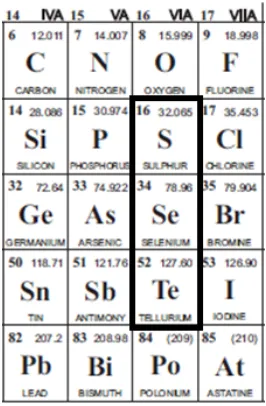
used chalcogenide material for PCRAM is Ge2Sb2Te5 (or GST) [21]. In this study, GST was used as the chalcogenide material. A typical cross-section of a GST phase-change device (or cell) is shown in Figure 1.2. Although there are a number of possible geometries for PCRAM cells [22], the geometry that was used is the “mushroom” structure shown (amorphous region marked by the * in Figure 1.2, left) [22].
Figure 1.2 Representation of a cross-section for a GST phase change device. Left: After RESET (mushroom structure); Right: After SET. Amorphous GST region marked by * in RESET image (LEFT image). TEM images courtesy of Micron Technology.
1.2.2 Operation
electrode. The small size of the bottom electrode is needed to promote the region around the bottom electrode to reach the highest temperature during operation in order to change the phase of the material. This region is sometimes referred to as the "active" or "melt" region of the PCRAM cell. Information is stored by exploiting two different solid-state phases (namely, the amorphous and the crystalline phase) of a chalcogenide alloy, which have different electrical resistivity. The amorphous (high-resistance) phase of the
chalcogenide glass has a disordered microstructure with little to no atomic order, and as a result the resistance range of the amorphous phase is between 1–10 MΩ, which is often 2 orders of magnitude higher than the crystalline (low-resistance) phase of the
chalcogenide glass, which has a resistance range between 10 -100 kΩ [22]. The change in the solid-state phase from the amorphous phase to the crystalline phase is based on the thermally-induced change in the active region of the chalcogenide GST layer [22], [24].
The phase-change of the PCRAM device to a highly resistive amorphous
chalcogenide material is accomplished when a voltage higher than the threshold voltage (Vth) is applied across the bit, driving a brief, intense current pulse through the device.
The RESET and SET pulses mentioned are illustrated in Figure 1.3, as a function of electrical current (I) and Time, with dotted lines representing the RESET and SET regions [25]. When the RESET pulse is applied, this raises the temperature of the
chalcogenide material above the melting temperature (i.e., Imelt which corresponds to T ~
The RESET operation creates the amorphous dome-shaped region (marked by the * in Figure 1.2, left) with a resistivity several orders of magnitude higher than that of the poly-crystalline region of the device, placing the device in a RESET state. To "SET" the device or recover the crystalline phase, an extended (longer duration: 100 ns – 1 µs range), low intensity, current pulse is applied to the phase-change material heating the device above the glass transition temperature (Icry, shown in Figure 1.3). The device is
then cooled more slowly, changing the phase of the material to a poly-crystalline (low-resistance) state [27]. It should be noted that the crystalline phase or SET state can also be achieved by annealing the amorphous GST at elevated temperatures. This is
accomplished through thermally-accelerated nucleation and/or growth of crystalline grains during the sub-melting annealing [18], which will be discussed further in Chapter 2.
Figure 1.3 Diagram of standard current pulses for PCRAM programming during writing (SET or logic 1) and Erasing (RESET or logic 0). Imelt refers to the current
pulse amplitude needed to achieve the melting temperature and Icry refers to current
Finally, to READ the state of the bit, a predetermined READ voltage is applied to the cell; and the current flowing through the device, referred to as the READ current, is sensed (current sensing approach). The READ voltage must be low enough to avoid unintentional modifications of the cell contents due to unintended heating during readout.
During the SET operation, there is a point where the resistance of the phase-change material drops suddenly. This phenomenon takes place at the threshold voltage (Vth) of the material and is often referred to as "snap-back,” “threshold switching,” or
“switching effect” of the device, due to the change in the current-voltage (I-V) trace. Figure 1.4 shows a typical I-V trace for the SET and RESET state. The I-V curve of the cell in its amorphous (or RESET) state shows an S-shaped behavior at about 1.2 V, which is the Vth for the measured device or the point where the conductivity of the cell changes
and becomes comparable to that of the SET state. This effect is due to the threshold switching phenomenon [20], [21], [24], which consists of a sudden drop in the
amorphous chalcogenide resistivity as the voltage reaches the threshold voltage (Vth) or
equivalently when the current flowing through the cell exceeds the threshold current value (Ith). From an application point of view, threshold switching plays an essential role
in the operation and performance of PCRAM cells; Vth defines the boundary between the
the Joule heating, resulting from the large current increase at switching, which for sufficiently long electrical pulses can contribute to the transition to the crystalline phase for glasses with low crystalline point [22],[34].
The programming operation of the PCRAM cell takes place in the high current regime of the SET and RESET trace, which is the location in Figure 1.4 where the amorphous (RESET) and crystalline (SET) I-V trace characteristics are almost indistinguishable (I = ~300 µA) [35].
Figure 1.4 Measured I-V curves for the crystalline (SET state) and amorphous (RESET state) chalcogenide [35].
1.2.3 Technology Development
mentioned in Section 1.2, PCRAM offers the possibility of improved scalability; the current state of the art is at the 20 nm technology node (cell half-pitch, F = 20 nm) with a cell size of 4 F2 (i.e., cell size = 4*(20 nm)2 ), as shown in Figure 1.5. Technology nodes are used to define the ground rules of device fabrication processes, governed by the smallest feature printed in a repetitive array [37].
Figure 1.5 Schematic of a memory cell array showing the cell size as 4 F2. Schematic image courtesy of Micron Technology.
device manufacturing or processing steps when compared to NAND and NOR. Moreover, the processing flow for PCRAM does not require the integration of ferroelectric and/or magnetic materials with the CMOS process flow, unlike FeRAM and STT-RAM.
Table 1.1 Comparison of non-volatile memories characteristics [8], [10], [38]– [40].
Among the companies that have invested in PCRAM technology, Micron is the first to supply high-volume availability of a 45 nm technology node, 1-Gigabit (Gb) LPDDR2, with an effective cell size of 5.5 F2 [36], [41], [42], in a multichip package. The technology development road map for PCRAM is reported in Figure 1.6, showing the aggressive technology scaling with each generation between Samsung and Micron
(formally Numonyx, STMicroelectronics).
The 180 nm technology node has been used as a vehicle to demonstrate and prove the viability of the technology, which for STMicroelectronics/Numonyx led to the
Figure 1.6 Technology development roadmap for PCRAM [36], [43]–[46].
1.3 Materials
Figure 1.7 Representation of a cross-section of the Micron 45 nm storage element architecture [36].
Since the phase change material (or memory layer) in the storage element is programmable with the application of an applied electrical pulse, when programming an array of devices, a selecting device is required in order to decoded the correct storage element inside the 1-Gb array of devices [22]. Two primary solutions have been investigated for high-volume manufacturing: 1) vertical Bipolar Junction Transistor (BJT) and 2) planar metal-oxide-semiconductor field effect transistor (MOSFET)
[22],[42], shown in Figure 1.8. Considering that the aim of process integration is to build a compact and efficient PCRAM storage element coupled with its selector, the BJT/Diode was considered to be an innovative solution for high density, high performance
Planar MOSFET Selector Vertical BJT Selector
Figure 1.8 Schematic Depiction Single Transistor Per PCRAM Cell Structure: Left: Planar Metal-Oxide Semiconductor Field Effect Transistor (MOSFET), Selecting Device; Right: Vertical Bipolar Junction Transistor (BJT), Selecting Device [42].
A comparison of the process complexity, size, organization, application, and the schematic of the MOSFET vs. BJT/Diode is shown in Figure 1.9. In this comparison, one can see that the cell size of the MOSFET is ~20 F2, while the BJT/Diode cell size was reduced to ~5 F2. As a result of the smaller cell size, the BJT/Diode-selector has been chosen in the 45 nm commercialized PCRAM part, which allows for higher performance and density applications [21], [42].
The PCRAM architecture was originally developed considering the small cell size requirements, the process cost, and the high performance characteristics, with the focus of obtaining fast random access-time typical of NOR Flash applications [22], [47]–[49]. The standard “µTrench” storage element fabrication steps proposed for the 90 nm technology platform is shown in Figure 1.10. For the standard “µTrench” storage element, one base-contact of the BJT/Diode is used for every emitter [36].
The active storage region is achieved at the intersection between the vertical thin-film metallic layer or heater (which is deposited inside an opening on a Tungsten (W) plug), and a thin layer of chalcogenide material (GST) capped with a TiN barrier (deposited inside a sub-lithographic trench or “µTrench”), as shown in Figure 1.10 [22],[42].
Figure 1.10 Schematic of the Self-aligned “µTrench” fabrication steps [42].
5.5 F2, leading to the design of the 1-Gb PCRAM product and “Wall” storage element, shown in Figure 1.11 [36].
Process module optimization, in particular an innovative double Shallow-Trench Isolation (STI) approach (used for isolation between adjacent emitters) and material improvements, have permitted the evolution of the cell from the “µTrench” (Figure 1.10) to the “Wall” structure (Figure 1.11), simplifying the overall storage element process integration and maintaining a very controlled low RESET current [36], [42]. The reliability results (discussed further in Chapter 2), using the new “Wall” cell have been very positive both in terms of retention and endurance; these results show that the
technology is able to meet the reliability expectations for 90 nm, 45 nm, and future scaled technology nodes [36], [42].
Figure 1.11 Schematic of the “Wall” storage element and related cross-sections [36].
1.4 Conclusions
CHAPTER 2: RELIABILITY
2.1 Reliability and Failure Rate
Reliability is one of the most important factors used to determine if a device fulfills its required functions for the prescribed period under the conditions for which it was designed. Each device has a lifetime, which is the length of time that the device works as desired. The reliability indicates the probability for functioning correctly without failure until time (tlife), which is used as a random variable for the lifetime of a
device in Equation 2.1. If the mission time (tmission) of the device is not specified, the
reliability of the device becomes a real-value function for tmission. It should be noted that
tmission is not a random variable. Then, the reliability function, R(tmission), which is the
probability that tlife is greater than tmission, can be formulated as follows:
𝑅(𝑡𝑚𝑖𝑠𝑠𝑖𝑜𝑛) = Pr�𝑡𝑙𝑖𝑓𝑒 > 𝑡𝑚𝑖𝑠𝑠𝑖𝑜𝑛�= � 𝑓(𝜃)𝑑𝜃,
∞
𝑡
(2.1)
where f(θ) is the probability density function (pdf) of tlife with respect to operating time θ.
Failure Rate (CFR), and 3) wear out failures or Increasing Failure Rate (IFR) [50]–[53]. It should be noted that the failure rate of semiconductors shows a gradual decreasing failure rate with increased time similar to the early “Infant Mortality” failure curve in Figure 2.1; hence, the longer a particular semiconductor device is used, the more stable it will be. However, two points must be considered regarding the service life of a device: 1) the CFR region, and 2) IFR region or the wear out of the device.
If a failure is caused by unrevealed manufacturing defects, it is classified as an early failure in the DFR region. Defects that do not materialize into yield losses can grow to failures during operation depending on the quantity of external and internal stresses [50], [52], [54]. These early failures are usually screened by accelerated life testing and burn-in [50]–[52].
Figure 2.1 Typical "Bathtub" curve for semiconductor devices [55].
2.2 Accelerated Life Tests
given failure mechanism, a common way of determining the presence of some stress (e.g., temperature cycling, electric field, current density) is through the acceleration factor. The mathematical relationship or equation commonly used for the acceleration factor due to changes in temperature for microcircuits and other semiconductor devices follows the format of the Arrhenius equation [50]. An example of the acceleration factor due to changes in temperature is shown in Equation 2.2:
𝐴𝑇 =𝜆𝜆𝑡
𝑠 = exp��
−𝐸𝑎 𝑘 � ∗ � 1 𝑇𝑡− 1 𝑇𝑠��, (2.2)
where Ea is the activation energy (in electronvolts (eV)), k is Boltzmann's constant
(8.62E-5 eV K-1), Tt is the absolute temperature of the test (in Kelvin), Ts is the absolute
temperature of the system (in Kelvin), λt is the failure rate at the test temperature, and λs
is the failure rate at the system temperature. The acceleration factor can be calculated for electrical, mechanical, environmental, and other stresses when those stresses affect the reliability of a device [50]. With accelerated testing, caution should always be used since the relationship only holds if the failure rate is constant; however, very few practical situations exist in which the failure rate is truly constant. Nevertheless, the assumption of constant failure rate is still commonly used.
2.3 PCRAM Reliability
2.3.1 Design Constraints
PCRAM [56], due to the instability of the amorphous GST [57], [22]. Early retention failures of the RESET bit have been related to pre-nucleation sites [56], which spur the rapid development of a conducting percolation path (shown in Figure 2.2), after a cell is RESET [18], [58].
Figure 2.2 Conducting percolation path of PCRAM: left, simulation example of retention failure by the formation of conducting percolation path, from t=0 to the formation of the path [58]; right (top), percolation path highlighted (red), the channel is made by a continuous low-Ea path; right (bottom), corresponding current
density profile, where the low-Ea path is the channel that brings the higher
percentage of the total current [18].
width is reduced, the GST is not able to fully crystallize, resulting in a higher SET resistance, limiting the READ margin or reading window between the SET and RESET states [22], [59]. It should be noted that it is unacceptable for high-performance products to have a SET pulse width of 10 µsec, thus requiring shorter pulses to be used, resulting in a trade-off or compromise between the READ margin and shorter SET pulse widths and the possibility of a SET cell not being sensed correctly during the READ pulse.
Figure 2.3 Programming curves of a MOSFET-selected PCRAM cell for different SET pulse widths [22],[59].
For the RESET pulse, shorter pulse widths have been found to be better, with advantages being seen in the PCRAM cell endurance, as shown in Figure 2.4. The theory behind the relationship between the cell endurance and the RESET pulse width is related to the overall time elapsed by the cell at higher temperatures during the RESET operation or the total energy dissipated inside the device [59]. It should be noted, that the
Figure 2.4 PCRAM cell endurance as a function of the RESET pulse width [59].
2.3.2 PCRAM Reliability Risks
The reliability risks of PCRAM can generally be grouped into three types: 1) data retention; 2) cycling endurance; and 3) data program and READ disturbs [56], [60], [61]. In Sections 2.3.2.1- 2.3.2.3, the standard methods used on the Micron 45 nm PCRAM devices to test the reliability risks are reviewed.
2.3.2.1 Data Retention
cells, which likely does not expose possible defect failure modes that may be
present/observed on a large array product [56]. For this reason, data retention needs to be examined at the part-per-million (PPM) level across a broad range of temperatures [56]. It should be noted that when the PCRAM device is subject to elevated temperatures, the resistance of the RESET PCRAM cell evolves with time as shown in Figure 2.5b [56], [57].
The behavior of the resistance shown in Figure 2.5 is mainly related to the unstable amorphous phase (RESET state) of the PCRAM cell, which is affected by two types of structural modifications: 1) the Structural Relaxation (SR) effect (Figure 2.5a), and 2) the crystallization process (Figure 2.5b) [57].
Figure 2.5 Resistance vs. time behavior during annealing, highlighting two possible structural phase modifications. (a) Structural relaxation at room temperature (T = 25 °C). (b) Drop in the RESET state cell resistance due to the nucleation and growth of a crystalline phase [57].
phenomenon seen in amorphous chalcogenides) [56]; however, crystallization in the amorphous phase eventually sets in resulting in a drop in resistance and thereby, loss of data in the cell [56], [63].
The Structural Relaxation (SR) only affects the amorphous phase and has been explained by defect annihilation in the amorphous network, as shown in Figure 2.6 by the schematical annihilation process for a dangling bond as it transitions to a more stable state [57].
Figure 2.6 Schematic for the structural relaxation model in the amorphous chalcogenide material: (a) Structural defects (point defect such as a dangling bond); (b) The transition to the more stable state requires thermal excitation over an energy barrier EA [57].
When multiple PCRAM cells are measured at the array level, a similar behavior is observed; however, the distribution of data retention failure times becomes broader. Figure 2.7 contains resistance distributions for an 512 Kb PCRAM array of RESET cells, which were run through successive high temperature bake steps [56]. The drift
resistance of the cells ranges from essentially SET (Resistance < 10 kΩ) to fully RESET (Resistance=1 MΩ) [56], and the percentage of cells moving toward the SET resistance increases with increased bake time.
Figure 2.7 Resistance distributions of initially RESET PCRAM cells with increasing bake time at elevated temperature [56].
To estimate failure rates at product use conditions, an acceleration model for retention loss as a function of bake temperature is often used [56]. The experimental procedure consists of: 1) placing arrays of cells in a RESET state, and 2) baking the cells at elevated temperatures until retention loss is observed [56]. The PCRAM cells are considered fails once the resistance drops below a specified threshold (~100 KΩ), which is repeated at multiple temperatures on the same cells [56]. Temperatures between 125 °C and 160 °C have been found to be sufficient to describe the failure using this process [56]. Once the data is collected, it is then fit to the Arrhenius equation (Equation 2.3) to determine the data retention time [56].
𝑡 ∝ 𝑒𝑥𝑝 �𝐸𝑎
While more complex models have been developed to describe the crystallization process, the simple Arrhenius model is able to describe the failure process over a range of temperatures as shown in Figure 2.8 [56].
Figure 2.8 Arrhenius plot of Data Retention Failure Time vs. Temperature, including both array and single cell data [56].
2.3.2.2 Cycling Endurance
As with data retention, achieving high reliability for cycling endurance is very important and requires optimized device and pulse operation [60]. The cycling endurance tests can be conducted in three ways: 1) SET cycling, 2) RESET cycling, and 3)
Figure 2.9 Cycling Endurance of a PCRAM cell [62].
When performing the cycling endurance tests, it should be noted that it is important that optimized programming pulses for SET and RESET be determined to ensure that the endurance of the device is maintained or improved [61]. It is also very important that the device is not over programmed as this can lead to early device failures such as: 1) “Stuck SET” or RESET fails, and 2) “Stuck RESET” or cell opens [60], [61]. In general, cells that get stuck in RESET after cycling show a higher threshold voltage, suggesting a failure mechanism related to the GST [60]. However, cells that get stuck in a SET state show a high resistance in the I-V curve at high current, suggesting that the failure mechanism is related to the heating element (or “heater element”) [60].
2.3.2.3 Data Program and READ Disturbs
disturb issues (related to the isolation between adjacent bits, shown in Figure 2.10), which can induce a transition from an amorphous state to a polycrystalline state in a PCRAM cell [62].
Figure 2.10 Left: Schematic description of the programming disturb phenomenon [62]; Right: TEM cross-section of aggressor (yellow) and disturbed cell (red); a portion of the amorphous GST dome is crystallized [64].
Disturbs are an intrinsic phenomena of the memory array [61]. There are two major disturb mechanisms: 1) thermal proximity disturb during programming, which are often referred to as “Data Programming Disturbs,” and 2) READ disturbs [61], [62]. Data programming disturbs occur when reading or writing a certain PCRAM cell, which then can effect unwanted reading or writing at a nearest neighbor PCRAM cell, or at PCRAM cells connected to the same word-line/bit-line as shown in Figure 2.10 [62]. For the READ disturbs, this often involves the repetitive readout of a PCRAM cell in a RESET state, which eventually may cause a modification of its phase.
To test for data programming disturbs, the following tasks are usually performed: 1) all cells in the array are programmed into a RESET state, 2) selected cells in a
RESET state resistance before and after on the cells that were not cycled are then compared to determine the number of cells affected by the programming disturb [61].
2.3.3 Bit Error Rate and Array Reliability
In order to integrate PCRAM devices into large and yielding arrays, a large READ margin or “reading window” between the two memory logic states must exist and be maintained, with a probability of error or Bit Error Rate (BER) less than 10-6 (1 PPM) [65]. An example of the “reading window” can be seen in Figure 2.11 where a single-tile (4 Mb distributions) of SET and RESET resistances were collected on the μTrench PCRAM array [65]. While the SET distribution is log-normal with a resistance of 5 - 10 kΩ, the RESET distribution is only log-normal for resistances between 400 kΩ - 1 MΩ. Starting around the cell resistance of ~400 kΩ a pronounced tail or “RESET tail” is shown, which extends toward the low-resistance value of 20 kΩ and narrows the reading window between the SET and RESET states [65]. This RESET tail has been related to PCRAM cells that may have some abnormal material properties in or around the GST cell as a result of defects or processing issues that causes the PCRAM cell to behave
Figure 2.11 Array statistics for 4 Mb of SET and RESET resistances collected on a μ-trench PCRAM array [65].
Looking at the resistance distribution for the SET and RESET states by cell percentage of 4Mb from an array of PCRAM devices (shown in Figure 2.11), it is apparent that the single electrical programming pulse used for the RESET operation is able to RESET the majority of the PCRAM cells. However, for the anomalous or
abnormal cells (within the lower 2.27% cell percentage), a different RESET pulse may be required to increase the RESET state resistance of these cells and improve the reading window between the SET and RESET states [65]. It has been found that an improvement of the RESET tail resistance distribution can be obtained by optimizing the RESET programming operation with a faster quenching time (tQ) on the RESET electrical pulse
as shown in Figure 2.12 and Figure 2.13, where tQ is varied from a 60 ns RESET pulse
Figure 2.12 RESET and SET current pulses and significant parameters (highlighting tQ or the quench time) [66].
With faster quenching time for the RESET pulse, the RESET tail becomes less apparent, meaning that the programming characteristics of the anomalous cells are now aligned with the intrinsic cell. This suggests that a faster quenching programming pulse is preventing the spontaneous crystallization of the PCRAM chalcogenide material, helping maintain the amorphous disordered state and high RESET resistance value [65].
Figure 2.13 Resistance distribution improvements: RESET achieved with a faster quenching of the RESET pulse (Green: longer quench time; Orange: Short shorter quench time); SET achieved with longer pulse (Green: Short pulse; Blue: long pulse) [65], [66].
activation energy are extremely important [67]. Single-cell characterization only allows for the modeling of the intrinsic cell reliability with no insight into the reliability behavior of large arrays. The correlation between single cell performance and array performance still needs to be better understood. For example, a recent study was completed that compared the cumulative distribution of a single cell and array of cells (shown in Figure 2.14) [67]. In this comparison, two distributions of the time to SET (t*set), which was
listed as the SET pulse-width required to reduce the cell resistance below 0.1 MΩ, were reviewed for: 1) The "Cell" distribution, which is a collection of multiple pulses on the same single cell, and 2) the "Array" distribution, which was obtained from a single SET pulse applied to multiple cells within the same array [67].
Figure 2.14 Cumulative distribution of measured set time t*set that is the
pulse-width of the set pulse required for reducing the cell resistance below 105 Ω. A cell distribution (collected from many experiments on the same cell) and array distribution (collected from single experiments performed on many different cells within the array) are compared [67].
interesting to see how the single cell distribution supports the repeatability of the crystallization process for a single cell [67].
2.4 Failure Rate Prediction
Several different distributions can be used to model failure rate under appropriate circumstances such as the exponential, Weibull, and lognormal distributions. However, it should be noted that due to the window of operating conditions chosen in this research (to be defined in Chapter 3). The standard time-to-failure or lifetime prediction methods and distributions commonly used are not possible, since the 45 nm 1-Gb PCRAM chip is not sufficiently stressed to fail at the temperatures and voltages, which are used for
determining the optimal pulse conditions for very long periods of time. For this reason, this reliability prediction method monitors the cell resistance distributions collected from sections of the PCRAM 1Gigabit (Gb) memory array and will predict a single
combination of temperature and pulse conditions, giving the lowest Bit Error Rate (BER).
2.4.1 Exponential Distribution
An exponential distribution implies a constant failure rate. However, a constant rate does not occur if the product is insufficiently screened or improperly designed for reliability. It also does not occur if the product is past the bottom of the “bath tub” curve and into the wear-out phase. The exponential distribution is the least complex of all lifetime distribution models. The exponential distribution for the reliability function is defined in Equation 2.4,
the cumulative distribution function (CDF) or failure distribution, is defined in Equation 2.5,
𝐹(𝑡) = 1− 𝑒𝑥𝑝(−𝜆 ∗ 𝑡), (2.5)
and the probability distribution function (PDF), or the lifetime distribution model, which is obtained from the derivative (with respect to time) of the CDF, is defined in Equation 2.6,
𝑓(𝑡) =𝜆 ∗ 𝑒𝑥𝑝(−𝜆 ∗ 𝑡), (2.6)
where, t is time and λ is the failure rate or “hazard rate.”
It should be noted that the mean time to failure (MTTF) of the exponential function is the inverse of the failure rate λ, which is defined in Equation 2.7.
𝑀𝑇𝑇𝐹 = 1/𝜆, (2.7)
In Figure 2.15-2.17, figures of the CDF, PDF, and hazard rate (λ), for the exponential distribution are shown.
Figure 2.16 PDF or f(t) for exponential distribution [68].
Figure 2.17 Exponential distribution hazard rate [68].
2.4.2 Weibull Distribution
𝑅(𝑡) = 𝑒𝑥𝑝 �− �[𝑡−𝛾𝛼 ]�𝛽�, (2.8)
where, β is the shape parameter, γ is the location parameter, which is also referred to as the defect initiation time parameter, and α is the characteristic life or scale parameter [68]. If failures do not start at time zero, the defect initiation time parameter (also known as the location parameter) is zero, and the Weibull exponential expression is reduced to Equation 2.9,
𝑅(𝑡) =𝑒𝑥𝑝 �− �𝛼𝑡�𝛽�, (2.9)
when β = 1, Equation 2.9 becomes the exponential model, with α = 1/λ or the MTTF. The PDF of the two parameter Weibull distribution is defined in Equation 2.10, a plot of the PDF is shown in Figure 2.19 for different values of β [68].
𝑓(𝑡) =𝛽𝑡�αt�β𝑒𝑥𝑝 �− �𝛼𝑡�𝛽�, (2.10)
The CDF of the two-parameter Weibull is defined in Equation 2.11,
𝐹(𝑡) = 1− 𝑒𝑥𝑝 �− �𝛼𝑡�𝛽�, (2.11)
Figure 2.18 CDF of Weibull function, varying β [68].
Figure 2.19 Weibull function PDF in units of α, varying β [68].
The cumulative failure rate of the two parameter Weibull model or so-called cumulative hazard rate is defined in Equation 2.12,
𝐻(𝑡) =�𝛼𝑡�𝛽, (2.12)
with the instantaneous failure rate defined in Equation 2.13.
ℎ(𝑡) =𝛽𝛼�𝛼𝑡�𝛽−1, (2.13)
2.4.3 Lognormal Distribution
The lognormal distribution is based on a normal distribution of failures vs. logarithm of time. The lognormal (also called Gaussian) distribution [68] for reliability function or survivor function is defined in Equation 2.14 as,
𝑅(𝑡) = 1− Φ �ln(𝑡)−ln(𝑡50)
𝜎 �, (2.14)
where,
Φ(𝑧) =12�1 +𝐸𝑟𝑓 �√2𝑧��. (2.15)
The characteristic fitting parameters are the time to 50% cumulative failure (t50) and sigma (σ), which is referred to as the shape parameter or the slope of the time to failure vs. the cumulative percent failure on a log scale and is a measure of the time dispersion of the failures [68]. The equation of the CDF for the lognormal distribution is shown in Equation 2.16.
𝐹(𝑡) = Φ �ln(𝑡)−ln(𝑡50)
The probability distribution function (PDF), or the lifetime distribution model, is defined in Equation 2.17,
𝑓(𝑡) =√2𝜋𝑡𝜎1 ∗ 𝑒𝑥𝑝 �−12 �ln(𝑡)− ln𝜎 (𝑡50)�2�, (2.17)
In Figure 2.21-2.23, figures of the CDF, PDF, and hazard rate, for the lognormal distribution are shown.
Figure 2.21 CDF of lognormal function with varying σ [68].
Figure 2.23 Hazard Rate of lognormal function with varying σ [68].
When performing reliability testing, the following points must be considered before implementing a reliability test: 1) in what applications will the device be used, 2) in what possible environments and operating conditions will the device be used, 3) what are the possible failure modes and mechanisms, 4) what level of reliability does the market require for the device, and 5) how long is the device expected to be in service. Once this is determined, there are multiple accelerated stresses that can be applied to devices such as: 1) temperature, 2) voltage, 3) temperature difference, and 4) current [51]. An important consideration in reliability testing is that the testing must contribute to the appropriate evaluation and improvement of semiconductor reliability [51].
2.5 Reliability Model Classification
shorten the test time, accelerated tests on voltage, temperature, and humidity have been developed. In addition, statistical sampling is used [50]–[53]. However, in recent years, customer demand for shorter development-to-shipment times as well as the increasing advancement and complexity of semiconductor devices has made failure analysis extremely difficult. Consequently, the evaluations of basic failure mechanisms are now being studied when a device is in the development phase. Products are divided into different test element groups such as process and design [51].
2.6 Proposal
The Micron/Numonyx 45 nm technology PCRAM production part will be used in mobile devices, such as smart phone and/or tablet. Considering the environment and the operating conditions that a mobile device is exposed to, if the mobile device were to be left in an automobile on a summer day, how many bits are at risk of being sensed incorrectly during the READ operation? Using the standard retention test discussed in Section 2.3.2.1, the retention prediction shows that the mobile device could sit in the car for 10 years and retain the state of the bit, if the ambient temperature of the car is below 85 °C. However, what if a programming pulse or READ pulse were applied multiple times while the mobile device was at an elevated temperature? How many PCRAM cells within the array would be at risk of possible retention loss, or what would be the
The hypothesis for this research is that a reliability prediction method that finds the optimal pulse conditions for an array of PCRAM devices (using ambient temperatures between 25 to 125 °C) and predicts the Bit Error Rate (BER) has the potential to predict reliability issues closer to the normal operating conditions for the device. In this work, the aim of this research is to develop a reliability prediction method, different than standard retention reliability methods, using lower ambient temperatures from 25 to 125 °C. This new method models and predicts a single combination of temperature and pulse
conditions that give the lowest Bit Error Rate (BER) on a 1-Gigabit (Gb) array of experimental PCRAM devices, using the Micron/Numonyx PCRAM 45 nm cell architecture.
2.7 Conclusions
CHAPTER 3: EXPERIMENTAL SETUP AND OPTIMAL PULSE CONDITION STRATEGIES
3.1 Experimental Setup
In Chapter 3 the experimental setup used for developing the reliability prediction method is presented. This includes the screening of the voltage pulse amplitude and SET quench time, which is later used to determine the design space for the designed
experiments. The prediction models are created for the optimal pulse conditions and Bit Error Rate (BER), which are then used to predict a single combination of temperature and pulse conditions giving the lowest Bit Error Rate (BER), on a 1-Gigabit (Gb) PCRAM array of Micron/Numonyx 45 nm PCRAM experimental devices.
3.1.1 Electrical Test Setup
In general, the most basic form of electrical testing for a single PCRAM device can be performed using a pulse generator (for programming the device) and an
oscilloscope to determine the voltage drop across the device (through the use of a series load resistor) [69]. For the Micron/Numonyx 45 nm PCRAM experimental chip, in order to access the 1 Gigabit (Gb) array, a device specific probe card and tester capable of making array level measurements is needed. The probe card is specifically designed for the Micron/Numonyx 45 nm PCRAM experimental chip to collect the electrical
devices depends on the shape of the programming pulse. For these reasons, all
measurements were performed using the MicroMate (µM) tester (Figure 3.1), which is a Micron specific tool that consists of a self-contained module offering the combination of both single cell and array level electrical characterization.
Figure 3.1 MicroMate (µM) Tester.
Depending on the part, the bond pads or electrical contact points between the PCRAM device and the pins of the probe card can change. For this reason, the package part probe cards are interchangeable on the probe stations, allowing multiple part types to be tested on the same probe station.
As shown in Figure 3.2, the device specific probe card can be inserted into a probe station just above the thermal chuck. Built-in clamps on the probe station are used to hold the package part probe card securely in place. The thermal chuck is used to hold the wafer in place by applying a vacuum on the back-side of the wafer; the thermal chuck also has electrical coils within the chuck, allowing the wafer to be heated for the
Figure 3.2 Probe station, showing package part probe card and thermal vacuum chuck (directly below the probe card).
As discussed in Chapter 1, each memory cell in the PCRAM array is referred to as a storage element. The storage element consists of a top electrode, memory layer (GST), and the heater storage element material. This storage element is connected to a BJT selection transistor, as discussed in Chapter 2 (shown in Figure 3.3, right). In the memory array, the base of all BJT select transistors is connected to the same row or “Word-Line,” while the top-electrode contacts the PCRAM cells belonging to the same column or “Line.” The memory cell is selected by means of row (or Word-Line) and column (or Bit-Line) decoders that generate the electrical control signals required for the READ and SET/RESET programming operations (shown in Figure 3.3, left).
It should also be noted that the Micron/Numonyx PCRAM 45 nm 1-Gb
mode (V-force) is used for the RESET pulse. For this reason, the optimal pulse conditions for the SET pulse using voltage mode (V-force) are not well understood on the
Micron/Numonyx 45 nm 1-Gb part. For all tests performed in the designed experiments (to be discussed), V-force is used for both the SET and RESET programming pulses.
Figure 3.3 Left: Diagram of PCRAM array [25], [42]; Right: Circuit schematic of an individual memory cell in the PCRAM array, Parasitics, Heater, Select Transistor, and programming pulse source.
In order to measure the cell current of the SET and RESET state with high accuracy, the PCRAM array can be operated in direct memory access (DMA) mode, allowing the cell current (Icell) to be sensed for a given bit within the array directly during
the READ operation. The cell resistance (Rcell) is calculated as the ratio between the
READ voltage (Vread), which is applied across the cell and the current sensed, which is
flowing through the cell Icell (i.e., Rcell = Vread / Icell).
3.1.2 The SET and RESET Pulse
In beginning, the process of determining the optimal programming conditions for the SET and RESET programming pulses, a key aspect that needed to be considered was the shape of the RESET and SET programming pulses. As described in Chapter 1, a proper RESET pulse requires a rapid quenching of the chalcogenide material to place the PCRAM cell in the amorphous or RESET state. For this reason, a square pulse was chosen for the RESET pulse operation, with the RESET pulse width fixed at 45 nsec and a trailing edge or quench time set at 10 nsec. The quench time of 10 nsec is the fastest reproducible pulse that can be applied to the 1-Gb PCRAM array with this tester.
For the SET pulse, a gradual trailing edge has proven to be more efficient when programming an array of devices into the crystalline or SET state [70], allowing the atoms within the chalcogenide material more time to arrange into a crystalline phase. For this reason, a trapezoidal, or “set-sweep,” form of pulse was implemented (shown in Figure 3.4). The set-sweep pulse is characterized by a maximum (VM) and minimum (Vm)
SET voltage, and the time before quench is labeled as Ts [70], which we will later refer to
as the SET quench time (Qs). In the literature, the set-sweep pulse of an array of PCRAM
of narrowing the SET distribution when programming multiple cells, due to the gradual change in the temperature profile [70].
Figure 3.4 Set-Sweep program pulse [70].
The theory behind the set-sweep pulse is that each cell has a specific optimum SET voltage for a determined programming time [70]. By using a trapezoidal SET pulse, different optimum SET voltages can be applied to different cells being programmed simultaneously; hence, if the optimal program voltage of a cell is in the range of (VM) to
(Vm), the cell turns out to be programmed with optimum conditions [70].
Prior to conducting the designed experiments, initial screening of the RESET pulse amplitude (Vr) and the SET quench time (Qs) were performed to determine the
window of values to use for the optimal pulse conditions Design of Experiment (DOE). The initial screening was performed to determine the high and low levels, which would be used for the DOEs as represented in the cube plots in Figure 3.5. In the Cube Plot shown (Figure 3.5, left), the left half of the two-dimensional geometric figure represents the observations of the cell resistance (Ri) collected when the RESET voltage (Vr) pulse
![Figure 1.4 Measured I-V curves for the crystalline (SET state) and amorphous (RESET state) chalcogenide [35]](https://thumb-us.123doks.com/thumbv2/123dok_us/8921979.1842413/29.612.170.471.289.531/figure-measured-curves-crystalline-state-amorphous-reset-chalcogenide.webp)
![Table 1.1 [40].](https://thumb-us.123doks.com/thumbv2/123dok_us/8921979.1842413/31.612.90.574.191.405/table.webp)
![Figure 1.6 Technology development roadmap for PCRAM [36], [43]–[46].](https://thumb-us.123doks.com/thumbv2/123dok_us/8921979.1842413/32.612.114.528.78.430/figure-technology-development-roadmap-pcram.webp)
![Figure 1.7 Representation of a cross-section of the Micron 45 nm storage element architecture [36]](https://thumb-us.123doks.com/thumbv2/123dok_us/8921979.1842413/33.612.118.534.72.315/figure-representation-cross-section-micron-storage-element-architecture.webp)
![Figure 1.8 Schematic Depiction Single Transistor Per Selecting Device; Right: Vertical Bipolar Junction Transistor (Left: Planar Metal-Oxide Semiconductor Field Effect Transistor (PCRAM Cell Structure: MOSFET), BJT), Selecting Device [42]](https://thumb-us.123doks.com/thumbv2/123dok_us/8921979.1842413/34.612.117.513.474.689/schematic-depiction-transistor-selecting-transistor-semiconductor-transistor-structure.webp)
![Figure 2.1 Typical "Bathtub" curve for semiconductor devices [55].](https://thumb-us.123doks.com/thumbv2/123dok_us/8921979.1842413/39.612.166.490.389.608/figure-typical-bathtub-curve-for-semiconductor-devices.webp)
![Figure 2.2 Conducting percolation path of retention failure by the formation of conducting percolation path, from t=0 to the formation of the path [58]; right (top), percolation path highlighted (red), the channel is made by a continuous low-Edensity profi](https://thumb-us.123doks.com/thumbv2/123dok_us/8921979.1842413/41.612.138.531.205.410/conducting-percolation-conducting-percolation-formation-percolation-highlighted-continuous.webp)
