RESEARCH NOTE
AN EFFICIENT TECHNIQUE FOR SUBSTRATE COUPLING
PARASITIC EXTRACTION WITH APPLICATION
TO RF/MICROWAVE SPIRAL INDUCTORS
Nasser Masoumi
Department of Electrical and Computer Engineering, University of Tehran Tehran, Iran, [email protected]
Mohamed I. Elmasry
VLSI Research Group, University of Waterloo Waterloo, Ontario, Canada, [email protected]
Safieddin Safavi-Naeini
Center for Wireless Communications, University of Waterloo Waterloo, Ontario, Canada, [email protected]
(Received: April 13, 2001 – Accepted in Revised Form: July 7, 2004)
Abstract This paper presents an efficient modeling method, based on the microstrip lines theory, for the coupling between a substrate backplane and a device contact. We derive simple closed-form formulas for rapid extraction of substrate parasitic. We use these formulas to model spiral inductors as important substrate-noise sources in mixed-signal systems. The proposed model is verified for the frequencies up to 35 GHz, and is easily adaptable to CAD tools.
Key Words Substrate Coupling, Microstrip Lines, Mixed-Signal, Spiral Inductors, CAD Tools
ﻩﺪﻴﻜﭼ
ﺍﻳ ﻪﻟﺎﻘﻣﻦ ﻳ ﻪﻳﺎﭘﺮﺑ،ﻱﺯﺎﺴﻟﺪﻣﺵﻭﺭﮏ ﺎﻣﻁﻮﻄﺧﻱﺭﻮﺌﺗﻱ
ﻳ ﮑ ﺳﺍﻭﺮ ﻱﺍﺮﺑ،ﭗﻳﺮﺘ ﻳﻭﺰﺗ
ﺮﺘﺴﺑ ﻦﻴﺑﺎﻣﺞ ﻳ
ﮏ
ﻪﻌﻄﻗ ﻚﻳ ﺢﻄﺳ ﻭ ﻪﺷﺍﺮﺗ ﻲﻣﻪﺋﺍﺭﺍ ﻱﺩﺎﻫ ﻪﻤﻴﻧ ﻱ
ﺩ ﺪﻫ
.
ﻝﻮﻣﺮﻓﺎﻣ ﻪﺘﺴﺑ ﻱﺎﻫ ﺮﺻﺎﻨﻋ ﻊﻳﺮﺳ ﻥﺩﺭﻭﺁ ﺖﺳﺪﺑ ﻱﺍﺮﺑﻱﺍ
ﻲﻣ ﺝﺍﺮﺨﺘﺳﺍ ﺮﺘﺴﺑ ﻲﮑﻴﺘﻳﺯﺍﺭﺎﭘ ﻛﻨ
ﻴ ﻢ
.
ﻢﻫ ﻒﻠﺳ ﻥﺩﺮﮐ ﻝﺪﻣﻱﺍﺮﺑ ﺍﺭﻂﺑﺍﻭﺭ ﻦﻳﺍ ﺎﻣ ﻦﻴﻨﭼ ﺯﺍ ﺩﻮﺧﻪﮐ ﻲﭽﻴﭘﺭﺎﻣ ﻱﺎﻫ
ﻢﺘﺴﻴﺳﺭﺩ ﻲﺠﻳﻭﺰﺗﺰﻳﻮﻧ ﻊﺑﺎﻨﻣﻦﻳﺮﺘﻤﻬﻣ ﻝﺎﻨﮕﻴﺳﻱﺎﻫ
-
ﻂﻠﺘﺨﻣ
)
ﻝﺎﺘﻴﺠﻳﺩ
-
ﮒﻮﻟﺎﻧﺁ
(
ﻲﻣﻩﺩﺎﻔﺘﺳﺍ ﺪﻨﺘﺴﻫ ﻢﻴﻨﮐ
.
ﻦﻳﺍ ﺭﺩ
،ﻪﻟﺎﻘﻣ ﺲﻧﺎﮐﺮﻓﻱﺍﺮﺑﻩﺪﺷﺩﺎﻬﻨﺸﻴﭘﻝﺪﻣ ﺎﺗﻱﺎﻫ
۳۵ ﻲﻣﺭﺍﺮﻗﻖﻳﺪﺼﺗﺩﺭﻮﻣﺰﺗﺮﻫﺎﮕﻴﮔ ﻩﺩﺎﻴﭘﻞﺑﺎﻗﻲﮔﺩﺎﺴﺑﻭﺩﺮﻴﮔ
ﻱﺯﺎﺳ
ﻡﺮﻧﻱﺎﻫﺭﺍﺰﺑﺍﺭﺩ ﻱﺭﺍﺰﻓﺍ
"
ﺮﺗﻮﻴﭙﻣﺎﮐﮏﻤﮐﻪﺑﻲﺣﺍﺮﻃ
"
(CAD) ﻲﻣ ﺪﺷﺎﺑ
.
1. INTRODUCTION
The current trend towards integrating analog and digital parts of a circuit on the same die forces mixed-signal system designers to take into account the problem of the substrate coupling in their models for simulation and optimization tasks. In addition, as the ICs clock speed increases and the technology feature length shrinks, the substrate noise adverse effect on the functionality of the circuit increases. Fast switching high-speed nodes in VLSI circuits can capacitively inject the signal,
so called substrate noise, into the chip substrate. Drain/source of MOS transistors, n+ buried layers
in BJTs, n-wells, substrate ties, and spiral inductors are examples of the substrate noise injection mechanisms [1]. Recently several methods of the substrate coupling modeling have been published in the literature [2], [3]. These methods generally encounter with huge model matrices, of which solutions require large computational times and a significant storage memory.
of monolithic spiral inductors. Spiral inductors can inject a significant amount of the substrate noise due to their large areas compared to other devices on the same die. In [4] the substrate of the spiral inductor has been modeled by a resistor, which is valid for the frequencies up to a few GHz [5]. In [6], [7] the substrate model has been extracted from measured data. Indeed, measured data is not required, if an appropriate and certain modeling method for the substrate is provided.
2. PRELIMINARIES
In this paper, we consider the chip substrate as a single-layer bulk substrate with a backplane. Commonly used substrates in ICs fabrication may have a thin (0.5 to 1 µm) channel stop implant at the top surface [2]. In lightly doped substrates the high-resistivity bulk is the only common substrate for all devices. On the contrary, heavily doped substrates consist of a high resistive epitaxial layer (with a height of 5 to 15 µm), and a low resistive bulk (with a height of 100 to 300 µm). However, the low resistive bulk can be assumed as a single node for the entire chip [8].
The backplane, which is attached to the backside of the die by conductive glue, is connected to the perfect ground. The simulation results and measurements reported in [9], [10], [11], [12] have proven the significance of using a backplane in the substrate coupling noise reduction especially for high frequency applications.
Contacts correspond to the areas where the designed circuit interacts with the substrate. Examples of these contacts include drain or source
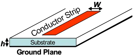
areas in MOS transistors, contacts from substrate or wells to supply lines, and contacts from passive devices, such as inductors and resistors, to the substrate. A conductive plate, as shown in Figure 1, models a device contact.
3. THE MICROSTRIP LINE APPROXIMATION METHOD
In some respects, the behavior of a device contact is similar to that of a microstrip line. In both structures, there is a substrate with a ground backplane and a conductor strip mounted on the top surface of the substrate. The conductor strip can be either of a metal type, or of a highly doped (low resistive) region. Figure 1 illustrates the geometry of a microstrip line.
If we assume a quasi-TEM mode of propagation in a microstrip line, the capacitance per unit length of the microstrip line, CM,is given by the following expression [13].
m 0 p M
Z v
1
C = (1)
where vp is the phase velocity and Z0m is the characteristic impedance of the microstrip line. However, the above equation for CM is theoretically valid for a microstrip line of an infinite length and for a pure TEM mode of propagation. In this study, the length of the contact on the substrate is always limited. The input source is applied to one edge of the contact, and the opposite edge is left open. Let us consider a rectangular contact of dimensions a and b, where a < b, and an input source is applied to the edge a. We model the substrate parasitic between the contact and the backplane by a parallel combination of a conductance Ga and a capacitance Ca in which the subscript a indicates the contact edge where the input source is applied to. The relative values of impedances due to Ga and Ca depend on values of the substrate resistivity p and the frequency f. In other words, we have ωC/G =ωε/σ. For instance, for ρ = 15 Ω-cm (σ = 6.66 Moho/m) we have ωε = 6.56 Moho/m. Therefore, the substrate capacitance and conductance are in the same order of
Co
ndu
cto
r S
trip
Ground Plane
h
W
Substrate
Ground Plane
h
W
h
W
Substrate
magnitude, so that both are necessary. Eventually, our modeling approach for Ca consists of three
steps as follows.
A. Step 0
We consider a segment of the length b of a long microstrip line of the width a. The total capacitance of this segment, CMab is given as CMab= bCMa where CMa is the capacitance per unit
length of the microstrip line and is given by (1). We have developed a program, which computes the characteristic impedance Z0m of any microstrip
line based on the rigorous formulas presented in [14]. The contact dimensions, the substrate specifications, and the frequency f are input variables to this program.
As a zero step approximation, Step 0, we assume a contact of the length b to be a segment of the above microstrip line. As a result, the total capacitance Ca of the substrate is approximated as
Mab
a C
C = (2)
B. Step 1
The total edge-capacitance of the two edges of the contact of the length b, Cedge_2b, isexpressed as below.
PP Mab b 2 _
edge C C
C = − (3)
where CPP is the parallel-plate capacitance between
the substrate and the backplane. It is computed
from CPP = ε0 εr A/h, where A is the contact area
and h is the substrate height.
Similarly, we consider a microstrip line of the width b. We denote its capacitance per unit length by CMb in which the subscript b implies the width
of the microstrip line. Therefore, the total capacitance of the length a of this microstrip, denoted by CMba, is given as CMba = aCMb, where
CMb is computed using equation (1). The total
edge-capacitance due to the two edges of the contact of the length a, Cedge_2a, is given as
PP Mba a 2 _
edge C C
C = − (4)
For a contact that the signal source has been applied to the edge a, the total edge-capacitance Cedge is computed as below.
a 2 _ edge b
2 _ edge
edge C 0.5C
C = + (5)
Finally, the total substrate capacitance Ca can be
expressed in the form
pp edge
a C C
C = + (6)
Substituting (5) into (6), and using (3) and (4), we obtain
) C C ( 5 . 0 C
Ca = Mab + Mba − PP (7)
In order to develop the model and investigate its accuracy, we define two parameters: the capacitance-factor KC as KC=Ca/CPP, and the
shape-factor ξ as ξ = A/h. Similarly, we define the conductance-factor KG as KG = Ga/GDC, where GDC
= (1/ρsub)(A/h). In [1] it has been shown that KG
and KC are functions of ξ, so that for any ξ in the
range of 0.01 < ξ < 10 and for the frequency range of 0.1 to 20 GHz, one can write KG(ξ) = KC(ξ). In
other words, KGand KC are constant functions of
the frequency. In addition, the maximum variations of CM in (1) with frequency for a wide range of
frequencies up to 35 GHz is less than 1%. As such, we assume Ca to be frequency independent.
Meanwhile, by extracting Ca we simply compute
Ga.
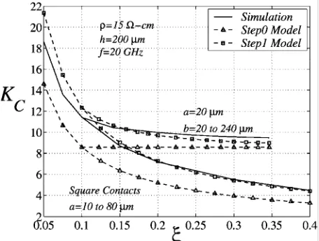
Figure 2 illustrates results of the modeling approaches Step0 and Step1. Results of the Step 0 approximation for square contacts deviate
Figure 2. Comparison of the modeling results using Step 0
considerably from the simulation results obtained from the numerical simulator IE3D where IE3D is a full-wave, method of moment electromagnetic simulator solving the current distribution on 3D and multilayered structures.. The relative error is within 40%. Compared to the Step0 approximation, the results obtained using the Step1 approximation are much closer to the simulation data. However, for small size square contacts and for rectangular contacts, the deviation of the Step 1 data from the simulation results are considerable and can reach to 19% (see Figure 2).
C. Step 2
The exact analytical solutions for an open-end capacitance of a contact result in double sums with large upper limits, or complicated integral equations [16]. To improve the accuracy of the model by using a more accurate approximation of the edge-capacitance Cedge, which also includeseffects of the open-end edge of the contact, we propose the following expression for Ca.
PP edge edge
a C C
C =λ + (8)
where
ξ −
⎟ ⎠ ⎞ ⎜ ⎝ ⎛ − =
λ 40
2
edge e
10 a 4 . 1 02 .
1 (9)
is a correction-factor for the edge-capacitance. We
have derived the above expression for λedge from
our experience and knowledge based on an extensive study of the simulation results.
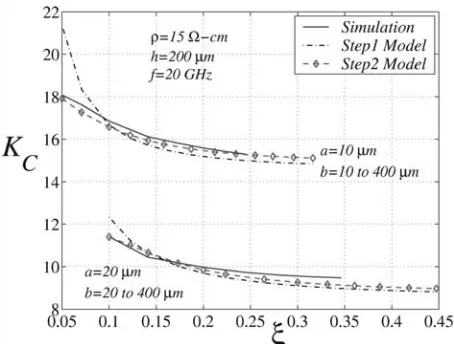
The plots in Figure 3 illustrate the comparison of simulation results with those of the models presented in Step1 and Step2 approximations. As Figure 3 shows, the modified model Step2 is better matched to the simulation results than the Step1 model. Particularly for small values of £ which correspond to small contact areas, our modified model is in very good agreement with simulation results, whereas the Step1 model deviates considerably. The accuracy of the modified model over 0.01 < ξ < 10 is better than 8%.
4. ADVANTAGES OF THE METHOD
Table 1 compares the results obtained by using our model MLAM (microstrip lines approximation method) with those presented in [2], [3]. As it is seen from the table, our modeling method is much faster compared to the other methods. In addition, the model is efficient for the memory usage. The model is accurate because it matches with rigorous simulations results of the full-wave simulator IE3D.
5. APPLICATION TO SPIRAL INDUCTORS
The exact modeling of spiral inductors is a necessary part of the design and verification
Figure 3. Comparison of results of the Step2 approximation
modeling approach with IE3D simulation results.
TABLE 1. Comparison of the Computation Times (on SUN UTRA 1/140) for Extraction of the Substrate Coupling Elements for a Single Contact Substrate.
Modeling Method Computatio n Time (sec)
Speedup Factor
Memory Usage
Green's Function
with DCT (M1) [2] 6.28 — 263 k Green's Function
Eigendecomposition
(M2) [3] Not Reported M2/M1=15 Required Microstrip Line
Approximation (M3) l,087 × 10-6
M3/M1=5,777
process of mixed analog-digital systems, because of the substrate noise impact of spiral inductors. Figure 4 illustrates the top view of a 4¼-spiral inductor and its cross section. The equivalent circuit model is depicted in Figure 5. This figure illustrates the circuit model in different levels denoted as Model-1, …, Model-n branch at the input port (Port-1).The Model-n is composed of n cascaded cells (a cell is shown as a shadow box in Figure 5) terminated parallel branch at the input port (port-1).
We have developed a program, which accurately computes the total spiral inductance LT and the total resistance RT utilizing the methods presented in [17] (including our modification) and [18], respectively. Moreover, we compute the substrate capacitance CTsub, and the oxide
capacitance CTox between the conductive layer and
the substrate, from the model formulas MLAM given in (8) and (9). The substrate conductance
GTSUB is computed from GTsub= KCGDC, which was addressed in the previous section.
We have also investigated modeling of effects of right-angle bends. In our study we have plotted the ratio of y-parameters of straight contacts to right-angled bent contacts with the same width W, area, and the same substrate parameters. In the simulations we have applied an input source to one port, while the other port is left open.
Figure 6 illustrates the ratio of imaginary part of the admittance of the straight contact to the bent contact, Rb = bs11/bb11 versus shape factor ξ for a
frequency range of 0.5 GHz to 35 GHz. As it is seen, the average of Rb is 1.071. An important
result achieved from this study is that, for a wide range of frequencies and for different values of the shape-factor ξ, the effect of a bend can be simply applied to the spiral inductor model as a factor Rb.
We have used the average value Rb = 1.07 to
improve the accuracy of the substrate model elements in Figure 5.
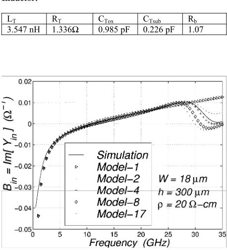
Figure 7 plots the input admittance Bin versus
frequency for the circuit depicted in Figure 5 (see Table 2 for the values). Since the spiral inductor is observed as a two port device, Bin is defined as Bin
= Imag[Iin/Vin] with output short circuited. As this
figure shows our model agrees with the IE3D results. The simple model shown as Model-1 is in good agreement with the rigorous simulation results up to 30 GHz. However, Model-4 better
Figure 6. Bend-effect ratio (Imag[y11straight]/Imag[y11bend]).
Figure 4. A 4¼-spiral inductor. (a) Top view. (b) Cross
section.
matches with the simulation results up to 35 GHz. Moreover the accuracy of Model-4 is better than 5% for the frequencies up to 20 GHz.
In addition, Figure 8 illustrates a comparison of
B21 = Imag [Y21] between our model and the
simulation results. B21 is defined as, B21 = Imag
[-Iout / Vin)] with output short-circuited. It is observed
from the figure that the proposed model better matches with the simulation results, as mentioned in the above.
6. CONCLUSIONS
We developed a novel, fast, and numerically efficient modeling method, based on the theory of microstrip lines, for the contact-to-substrate coupling. The model is presented in terms of simple closed-form formulas, and is suitable for implementing in CAD tools.
As an important application to RF and mixed analog-digital systems, we employed the proposed model for spiral inductors. Meanwhile, in order to improve the spiral inductor model we addressed the bend effects. The accuracy of the model was validated by comparison with IE3D simulation re-sults up to 35 GHz.
7. ACKNOWLEDGEMENT
This work was supported by the Ministry of Science, Research and Technology (MSRT) of Islamic Republic of Iran, and by Communications & Information Technology Ontario (CITO).
8. REFERENCES
1. Masoumi, N., “Fast and Efficient Modeling Methods for Substrate Coupling in VLSI Circuits”, PhD Thesis, VLSI Research Group, University of Waterloo, (2001). 2. Gharpurey, R. and Meyer, R. G., “Modeling and Analysis
of Substrate Coupling in Integrated Circuits”, IEEE Journal of Solid-State Circuits, Vol. 31, (March 1996),
344-352.
3. Costa, I. P., Chou, M. and Silveira, L. M., “Efficient Techniques for Accurate Modeling and Simulation of Substrate Coupling in Mixed-Signal IC’s”, IEEE Trans, on Computer-Aided Design, Vol. 18, (May 1999),
597-607.
4. Burghartz, I. N., Edelstein, D. C., Lenkins, K. A., Lahnes, C., Uzoh, C., O'Sullivan, E. I., Chan, K. K., Soyuer, M., Roper, P. and Cordes, S., “Monolithic Spiral
TABLE 2. Values of the Circuit Model for the 4¼-Spiral Inductor.
LT RT CTox CTsub Rb 3.547 nH 1.336Ω 0.985 pF 0.226 pF 1.07
Figure 7. Comparison of Imag [Yin] of Model-n with IE3D
simulation results.
Inductors Fabricated Using a Vlsi Cu-Damascene Interconnect Technology and Low-Loss Substrates”,
Proc. of IEEE Int. Electron Device Meeting, (1996),
99-102.
5. Stanisic, B. R., Verghese, N. K., Carley, L. R. and Allstot, D. I., “Addressing Substrate Coupling in Mixed-Mode IC’s: Simulation and Power Distribution Synthesis”, IEEE Journal of Solid-State Circuits, Vol.
29, (March 1994), 226-238.
6. Yue, C. P., Ryu, C., Lau, I., Lee, T. H. and Wong, S. S., “A Physical Model for Planar Spiral Inductors on Silicon”, Proc. of IEEE Int. Electron Device Meeting, (1996), 155-158.
7. Pun, A. L. L., Yeung, T., Lau, I., Clement, F. I. R. and Su, D. K., “Substrate Noise Coupling Through Planar Spiral Inductor”, IEEE Journal of Solid-State Circuits, Vol. 33, (June 1998), 877-884.
8. Su, D. K., Loinaz, M. I., Masui, S. and Wooley, B. A., “Experimental Results and Modeling Techniques for Substrate Noise in Mixed-Signal Integrated Circuits”,
IEEE Journal of Solid-State Circuits, Vol. 28, (April
1993), 420-430.
9. Masui, S., “Simulation of Substrate Coupling in Mixed-Signal MOS Circuits”, Dig. of Tech. Papers IEEE Int. Symp. on VLSI Circuits, (1992), 42-43.
10. loardar, K., “A Simple Approach to Modeling Cross-Talk in Integrated Circuits”, IEEE Journal of Solid-State Circuits, Vol. 29, (October 1994), 1212-1219.
11. Viviani, A. Raskin, I. P., Flandre, D., Colinge, I. P. and Vanhoe-nacker, D., “Extended Study of Crosstalk in SOI-SIMOX Substrates”, IEDM, (1995), 713-716.
12. Verghese, N. K., “Extraction and Simulation Techniques for Substrate-Coupled Noise in Mixed-Signal Integrated Circuits”, PhD Thesis, Carnegie Mellon University, (August 1995).
13. Gonzalez, G., Microwave Transistor Amplifiers”, Prentice-Hall, Second Ed., (1997).
14. Hammerstad, E. and Lenson, O. "Accurate Models for Microstrip Computer-Aided Design”, IEEE MTT-S Int. Microwave Symp. Dig., (1980), 407-409.
15. Masoumi, N., Elmasry, M. I. and Safavi-Naeini, S., “A Fast Parametric Model for Contact-Substrate Coupling”,
In International Conference on VLSI'99, Portugal,
Lisbon,(December 1999), 69-76.
16. Gupta, K. C., Garg, R., Bahl, I. and Bhartia, P., “Microstrip Lines and Slot-lines”, Artech House Publishers, Second Ed., (1996).
17. Greenhouse, H. M., “Design of Planar Rectangular Microelectronic Inductors”, IEEE Transactions of Parts,
Hybrids and Packaging, Vol. PHP-10, (June 1974), 101-109.
18. Pettenpaul, E., Kapusta, H., Weisgerber, A., Mampe, H., Luginsland, I. and Wolf, I. “Cad Models of Lumped Elements on Gas Up to 18 GHz”, IEEE Trans, on Microwave Theory and Techniques, Vol. 36, (February
![Figure 6. Bend-effect ratio (Imag[y11straight]/Imag[y11bend]).](https://thumb-us.123doks.com/thumbv2/123dok_us/243538.2019060/5.595.310.537.85.257/figure-bend-effect-ratio-imag-straight-imag-bend.webp)