Please cite this article as: N. M. Dyamannavr, N. G. kurahatti,A. Christina, Design and Implementation of Field Programmable Gate Array Based Baseband Processor for Passive Radio Frequency Identification Tag, International Journal of Engineering (IJE), TRANSACTIONS A: Basics Vol. 30, No. 1, (January 2017) 127-133
International Journal of Engineering
J o u r n a l H o m e p a g e : w w w . i j e . i r
Design and Implementation of Field Programmable Gate Array Based Baseband
Processor for Passive Radio Frequency Identification Tag
N. M. Dyamannavr*a, N. G. kurahattib,A. Christinaa
a Govt. Engineering College Engineering Kushalnagar, Karnataka, India b East point College of Engineering and Technology, Bangalore Karnataka, India
P A P E R I N F O
Paper history:
Received 18 July 2016
Received in revised form 12 September 2016 Accepted 05 January 2017
Keywords:
Radio Frequency Identification Base Band Processor
Hardware Descriptive Language Field Programmable Gate Array
A B S T R A C T
In this paper, an Ultra High Frequency (UHF) base band processor for a passive tag is presented. It proposes a Radio Frequency Identification (RFID) tag digital base band architecture which is compatible with the EPC C C2/ISO18000-6B protocol. Several design approaches such as clock gating technique, clock strobe design and clock management are used. In order to reduce the area Decimal Matrix Code (DMC) technique is used. The digital base band processor has been simulated and implemented using Xilinx platform. The complete design is verified and tested on Spartan-6 Field Programmable Gate Array (FPGA) board. The performance of system is measured in terms of power. The synthesis result shows that, the power required for complete design of digital baseband processor is 5mW on a supply voltage of 1.2 V.
doi: 10.5829/idosi.ije.2017.30.01a.16
1. INTRODUCTION1
Radio Frequency Identification (RFID) is “An automatic identification technology that uses radio frequency signals to transmit the identity of objects in the form of a unique serial number”. This technology does not use line of sight for communication between reader and tag. It is the best choice for automatic identification due to factors like flexibility, ease of use, contactless, multiple tag identification, high data rate, long read range and low cost. RFID application is growing in many fields such as smart table, access control, animal tracking, logistics, supermarkets, airport baggage handling, antifraud systems and medical treatment [1-5].
RFID system consists of reader, tag and an antenna. The reader has antenna that sends/receives radio frequency signals to/from tags. Tag shares the data with the reader through radio frequency signals. The main component of the tag is digital base band processor
1*Corresponding Author’s Email: [email protected] (N. M.
Dyamannavr)
which controls all the functions of the tag. Several tag digital base band designs have been presented before namely, Tag in Dingguo. Wei et al. [6] presented a paper on a “digital base band processor for passive UHF RFID tag” with reduced power consumption and chip area. The low power design techniques involved were low operating frequency, power management with clock gating and asynchronous design in which power consumption was about 2.7 μW with area of 0.11mm2. Jose et al. [7] presented the design of a baseband processor architecture with low-power design strategies such as clock gating and clock managing for a passive RFID transponder and communication link between reader and tag operates based on EPC class-1 Generation-2 protocol with master frequency of 1.92 MHz and current consumption of about 2.9 μA.
The challenge in designing UHF passive RFID tag is to reduce power consumption because the energy of a passive tag comes from the signal sent by a reader which is a power limited device. The operation range of a RFID system depends on the maximum of the dynamic power of the tag. There are static power dissipation and dynamic power dissipation in the very-large-scale integration (VLSI) circuit. Dynamic power
dissipation includes switching power due to charge and discharge of load capacitance of input signals. Static power dissipation results from the leakage current when the logic gate is static [8]. To reduce power consumption in RFID tag, there is a need to focus on dynamic power dissipation.
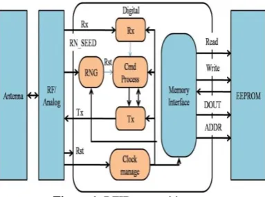
Figure 1 shows the architecture of the passive UHF RFID tag which consists of four sections: the antenna, RF/Analog section, digital section and electrically erasable programmable read only memory (EEPROM). The antenna is used for receiving and transmitting signals through the air interface. The received signal will be demodulated by the RF/Analog front end. Digital section is a base band processor of the tag. It consists of three sections. They are: Transmitter, Receiver and Processing section. Digital base band processor performs decoding, cyclic redundancy check (CRC) checking, processing, accessing memory, encoding message and transmitting data back to reader.
In this proposed paper, we have developed a digital base band processor for UHF tag which includes, encoding, and decoding architecture compatible with ISO/IEC 1800-6 tag on Spartan-6 FPGA and then its functionality is observed. The base band processor modelling is developed by Model Sim and is implemented and verified on Spartan-6 FPGA board.
This paper is organized as follows: Section 2 defines the architecture of the proposed design. Section 3 explains power optimization techniques. Section 4 describes simulation and synthesis results. Finally section 5 presents the conclusion.
2.ARCHITECTURE OF THE PROPOSED DESIGN
The proposed design of base band processor is shown in Figure 2. It is divided into several sub modules such as Encoder module, CRC module and error corrector module at the transmitter section and frame generator, decoder and buffer at receiving section. The processing section consists of command processing, memory interface and EEPROM.
Figure 1. RFID tag architecture
Enable input acts as a control input to each module. Each sub modules has to set the enable output when they complete their operation for clock gating purpose. The used decoder is decimal matrix coding (DMC) decoding which calculates the ‘H’ and ‘V’ from the received data bits do-d31 and generates cont module, and
removes from decoder block. CRC module calculates syndrome bits ∆𝐻 and 𝑆 according to DMC decoder. If syndrome bits are not equal to zero, then, it performs the error correction, otherwise not. Command processing recognizes command which is given in received data. It is identified using D16 bit in data. If the D16 bit is 0, it
generates a read signal to fetch the memory for sending tag ID number and if D16 is 1, then, it generates write
signal and writes data into memory. Buffer is used to store, the fetched 32-bit tag ID number and applied to the encoder. Encoder is used in DMC encoding which generates horizontal and vertical redundant bits with the data bits. Frame generator generates the frame in which data has to be sent.
Encoder performs the DMC encoding and generates horizontal, vertical redundant bits with the data bits. Frame generator generates the frame in which format data is being sent.
2. 1. DMC Encoder In the proposed design, DMC encoder is used, which uses decimal algorithm to increase the error detection and correction capability. In this algorithm power consumed will be less compared to other detection methods. This algorithm involves decimal integer subtraction and integer addition. In the decimal algorithm, the divide-symbol and arrange-matrix are performed. Here the N-bit word is divided into n symbols of m bits (𝑁 = 𝑛 × 𝑚), and these symbols are arranged in an n= 𝑛1 × 𝑛2 2-D matrix, the horizontal redundant bits ‘H’ are obtained by performing decimal integer addition on symbols per row. Finally, the vertical redundant bits ‘V’ are obtained by binary operation on the bits per column. It is noted that both divide-symbol and arrange-matrix are presented in logical instead of physical form.
To explain the DMC scheme, take a 32-bit word as input, which is shown in Figure 3. The cells from D0 to
D31 are information bits. This 32-bit word has been
divided into eight symbols of 4-bits. n1=2 and n2=4 have
been chosen simultaneously.𝐻0− 𝐻19 are horizontal
check bits;V0 through V15 are vertical check bits.
The horizontal redundant bits H can be obtained by decimal integer addition as follows:
𝐻4𝐻3𝐻2𝐻1𝐻0= 𝐷3𝐷2𝐷1𝐷0+ 𝐷11𝐷10𝐷9𝐷8 (1)
𝐻7𝐻6𝐻5 = 𝐷7𝐷6𝐷5𝐷4 + 𝐷15𝐷14𝐷13𝐷12 (2)
Similarly other remaining horizontal redundant bits are obtained where “+” represents decimal integer addition. For the vertical redundant bits V, we have:
𝑉0 = 𝐷0⊕𝐷16 (3)
𝑉1 = 𝐷1⊕𝐷17 (4)
In a similar manner remaining vertical redundant bits are obtained. The encoding can be done by decimal and binary addition operations from (1) to (4). The encoder that computes the redundant bits using multi-bit adders and XOR gates is shown in Figure 4. In this figure, H19−H0 are horizontal redundant bits, V15−V0 are
vertical redundant bits, and the remaining bits U31−U0
are the information bits which are directly copied from D31 to D0.
2. 2. DMC Decoder For the correction of word obtained, the decoding process is required. At the
beginning, the received redundant
𝐻4𝐻3𝐻2𝐻1𝐻0′ and 𝑉0′ − 𝑉3′ are generated by the
received information bits D’.
Figure 3. 32-bits DMC logical organization [8]
Figure 4. 32 bit DMC encoder structure using multi bit adders
and XOR gate [9]
Secondly, the horizontal syndrome bits 𝐻4𝐻3𝐻2𝐻1𝐻0
and the vertical syndrome bits S3 −S0 can be calculated as follows:
△ 𝐻4𝐻3𝐻2𝐻1𝐻0′=𝐻4𝐻3𝐻2𝐻1𝐻0′ − 𝐻4𝐻3𝐻2𝐻1𝐻0 5
𝑆0 =𝑉0′⊕𝑉0 6
Similarly for the remaining vertical syndrome bits, “−” represents decimal integer subtraction. When △ 𝐻4𝐻3𝐻2𝐻1𝐻0 ′ and 𝑆3− 𝑆0 are equal to zero, the stored
codeword has original information bits in symbol 0 are nonzero, then there is an error. Induced errors are detected and located in symbol 0 and these errors can be corrected by:
𝐷0𝐶𝑜𝑟𝑟𝑒𝑐𝑡= 𝐷0⊕𝑆0 7
The DMC decoder used in our design is shown in Figure 5, which consists of syndrome calculator, error locator, and error corrector. Here, each module performs a particular function in the decoding process. It is noted from Figure 5, that the redundant bits are obtained from the received information bits ‘D’ and compared with the original set of redundant bits in order to obtain the syndrome bits △ 𝐻 and S. Then, error locator uses △ 𝐻
and S to detect and locate error bits. Finally, the error corrector corrects the error bits by inverting the values of error bits. The ‘En’ signal is used to decide whether encoder is a part of the decoder.
3.LOW POWER DESIGN TECHNIQUES
According to Synopsys’s power model, the equation of the dynamic power is given by:
P = 0.5. α. CL. VDD2. f (8)
hereCLdenotes the total load capacitance of circuit, ‘α’
represents the switching activities, f is the frequency of circuit operation, and VDDrepresents the power supply
voltage.
In this paper to reduce the power consumption of the RFID tag is based on the above equation.
3.1. Low Operating Frequency The dynamic
power consumption of tag design is directly proportional to its clock frequency. The lower the clock frequency, the lesser is the power consumption. In our design we use digital clock manager to divide the clock into the two clocks of lower frequency and these frequencies are applied to the corresponding modules.
3. 2. Power Management With Clock Gating In
conventional synchronous design, all the sequential circuits consume power every clock cycle. However, all sub-modules are not performing a useful function, while they dissipate much power. Disabling the clock of
unnecessary sub-modules can reduce power
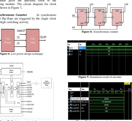
significantly. These techniques are shown in Figure 6. Clock manager divides the input clock frequency into f/2 and f/3 which are input to the clock gating block. Clock gating block has three inputs such as f/2, f/3 and enable input. According to the enable input, the clock gating module gives the specified clock to the corresponding module. The circuit diagram for clock manger is shown in Figure 7.
3. 3. Asynchronous Counter In synchronous counter, all flip-flops are triggered by the single clock and have a high switching activity.
Figure 6. Low power design technique
Figure 7. Clock manger circuit diagram
In asynchronous design, as Figure 8 shows, the next bit flip-flop is triggered by the output of preceding bit and it reduces the unnecessary switching activities and in the mean while the power consumption is low.
4. SIMULATION AND SYNTHESIS RESULTS
The proposed design has been done in Verilog HDL; simulated using model Sim simulator. For synthesis, we have used the EDA tool Xilinx and all sub module simulation results and top module results are shown in the following sections. Figure 9 shows the simulation result and of encoder module. Input is a 32-bit tag ID number and generates 20-bit horizontal and 16-bit vertical redundant numbers as output.
Figure 10 shows the simulation result of transmitter module. The 32-bit tag ID number is input to this module. It generates an output frame of 68-bit length. The frame contains 16-bit vertical redundant number, 20-bit horizontal redundant number and 32-bit input.
Figure 8. Asynchronous counter
Figure 9. Simulation result of encoder
Figure 11 shows simulation result of encoder in receiver. The received data may be corrupted due to the transmission error. So, the error data is given to this module as an input, then it generates 20-bit horizontal redundant bits and 16-bit vertical redundant bits derived from error data as an output.
Figure 12 shows the simulation result of CRC module, to check whether the received data bits are correct or not. It calculates the vertical syndrome bits by XORing the original vertical V [15-0] bits with the vertical bits being derived from received data Vd [15-0].
Figure 13 shows the simulation result of CRC module, to calculate horizontal syndrome and whether the received data bits are corrupted or not. It calculates the horizontal syndrome bits by subtracting the original horizontal H [19-0] bits with the horizontal bits which are derived from received data Hd [19-0]. If it is
non-zero value the data is corrupted otherwise it is not corrupted.
Figure 11. Simulation waveform of encoder in receiver
Figure 12. Simulation result of CRC for vertical syndrome
bits
Figure 13. Simulation result of CRC for horizontal syndrome
bits
Figure 14 shows simulation result of corrector, the 32-bit error data, computed 20-32-bit horizontal syndrome 32-bits and 16-bit vertical syndrome bits given as an input to the model. It generates an output of corrected 32-bit data.
Figure 15 shows the simulation result of receiver module, the 68-bit frame is input and generates 32-bit decoded data as an output. It performs the data correction if it is required. This module is comprised of CRC and error corrector modules.
Figure 16 and Table 4. 2 shows the simulation result. It consists of all sub modules such as encoder, decoder, CRC checker, error corrector, frame generator and buffer. It fetches the 32-bit tag ID number stored in ROM memory, performs encoding, frame generating, decoding, error corrections and generates fetched 32-bit tag ID as output.
Table 1 shows area comparison summary of the DMC technique. It indicates that DMC technique performance is better in terms of area when compared with other publications.
Figure 14. Simulation waveform of corrector
Figure 15. Simulation result of receiver
TABLE 1. Area comparison summary of the DMC technique
Name Ref. [13] Ref. [14] work This Optimization %Area
No. of slices 75 38 15 40%
No. of flip-flops 100 50 15 30%
No. of LUTs 132 68 14 21%
No. of logic 196 50 13 26%
No .of IOS 72 56 44 79%
No. of bounded IOB 72 40 44 ----
No. of GCLK 1 1 1 0%
Total 584 321 146 45%
Various other parameters such as delay and power summary for DMC technique are shown in Table 2 for various ECC’s. This technique has better performance in terms of power and speed.
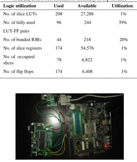
The device utilization summary of top module for complete design of the passive RFID Tag is shown in Table 3.
TABLE 2. Power and delay comparison summary of the
DMC technique
Type of ECC used
Slice flip
flops LUTs
Bounded IO
Delay
(ns) Power
This work 174 30 96 44 3.10ns 0.5mW
DMC [8] NA NA NA NA 4.9ns 10.8mW
PDS* NA NA NA NA 18.7ns 221.1mW
MC NA NA NA NA 7.1ns 24.7mW
Matrix
code 164 32 291 96 14.548ns 0.121W
Hamming
code 1350 32 2682 84 17.133ns 0.163W
PIE/FM0 NA NA NA NA NA 1.58mW
Comparison with some researches in base band processor of EPC C1G2 protocol-based UHF RFID tag is shown in Table 4. It indicates that our base band processor has better performances in terms of power, area and speed.
Figure 17 shows the hardware implementation of the complete design on FPGA Spartan-6, where, the ID number is read from ROM. Initially, error is detected, corrected, encoded and decoded. It is successfully downloaded and verified on the FPGA Spartan -6 board.
TABLE 3. Device utilization summary of top module
Logic utilization Used Available Utilization
No. of slice LUTs 208 27,288 1%
No. of fully used 96 244 39%
LUT-FF pairs
No. of bonded IOBs 44 218 20%
No. of slice registers 174 54,576 1%
No. of occupied
slices 78 6,822 1%
No. of flip flops 174 6,408 1%
Figure 17. Shows the hardware implementation of the
complete design display FPGA device
TABLE 4. Comparison summary of the design
Ref. No Technology Tag Type Coding Method Input Clock Supply Voltage Power Area
This Work Xilinx FPGA Passive DMC 100 MHz 1.8V * 5 mW 78 (slices)
[8] CMOS Technology Passive PIE/FM0 3.55 MHz 1.8V 3.43 μW 892 μm ×260μm
[6] CMOS Technology Passive PIE/FM0 1.92 MHz 1V 2.7 μW 0.11mm2
[10] CMOS Technology Passive PIE/FM0 1.92 MHz 1.2V 3.5 μW NA
[11] CMOS Technology Passive PIE/FM0 1.92 MHz 0.33V 80 nW NA
[12] CMOS Technology Passive PIE/FM0 2.56 MHz 1V 6.4 μW 0.3 mm2
[7] CMOS Technology Passive PIE/FM0 3.55 MHz 0.96V 7.4 μW 800 μm× 800μm
[13] FPGA Passive PIE/FM0 2 MHz 2V 9 mW NA
5. CONCLUSION
In this paper, the digital base band processor for UHF passive RFID tag has been presented. Several methods have been adopted in the design of the processor in order to optimize the power consumption, improve the area and speed. The complete design is tested and verified on Spartan-6 FPGA prototype board. Simulation and synthesis results reveal that our base band processor can complete its function successfully with a low power consumption of about 5 mW on 1.2 V supply voltage.
6. REFERENCES
1. Landt, J., "The history of rfid", IEEE Potentials, Vol. 24, No. 4, (2005), 8-11.
2. Nath, B., Reynolds, F. and Want, R., "RFID technology and applications", IEEE Pervasive Computing, Vol. 5, No. 1, (2006), 22-24.
3. Weinstein, R., "RFID: A technical overview and its application to the enterprise", IT Professional, Vol. 7, No. 3, (2005), 27-33. 4. Finkenzeller, K. and Handbook, R., Fundamentals and applications in contactless smart cards and identification, chicester. (2003), Sussex, UK: John Wiley.
5. Ismail, I. and Ibrahim, A., "Modeling and simulation of baseband processor for UHF RFID reader on fpga",
International Journal of Electrical and Electronic Systems
Research, Vol. 6, (2013), 54-66.
6. Wei, D., Zhang, C., Cui, Y., Chen, H. and Wang, Z., "Design of a low-cost low-power baseband-processor for UHF RFID tag with asynchronous design technique", IEEE International Symposium on Circuits and Systems, IEEE., (2012), 2789-2792. 7. Jinpeng, S., Xin'an, W., Shan, L., Hongqiang, Z., Jinfeng, H., Xin, Y., Xiaoxing, F. and Binjie, G., "Design and implementation of an ultra-low power passive UHF RFID tag",
Journal of Semiconductors, Vol. 33, No. 11, (2012), 115011. 8. Man, A.S., Zhang, E.S., Chan, H., Lau, V.K., Tsui, C. and
Luong, H.C., "Design and implementation of a low-power baseband-system for RFID tag", EEE International Symposium on Circuits and Systems, IEEE. (2007), 1585-1588.
9. Guo, J., Xiao, L., Mao, Z. and Zhao, Q., "Enhanced memory reliability against multiple cell upsets using decimal matrix code", IEEE Transactions on Very Large Scale Integration (VLSI) Systems, Vol. 22, No. 1, (2014), 127-135.
10. Rodriguez-Rodriguez, J.A., Delgado-Restituto, M. and RodrIguez-VAzquez, a., "Baseband-processor for a passive uhf RFID transponder", in Green Circuits and Systems (ICGCS), International Conference on, IEEE. (2010), 344-348.
11. Shi, W., Choy, C.-S., Guo, J., Chan, C.F., Leung, K.N. and Pun, K.P., "A 90nm RFID tag's baseband processor with novel pie decoder and uplink clock generator", 53rd IEEE International Midwest Symposium on Circuits and Systems, (2010), 644-647. 12. Roostaie, V., Najafi, V., Mohammadi, S. and Fotowat-Ahmady,
A., "A low power baseband processor for a dual mode uhf epc gen 2 RFID tag", in Design and Technology of Integrated Systems in Nanoscale Era. DTIS. 3rd International Conference on, IEEE. (2008), 1-5.
13. Chen, G. and Li, L., "Design of digital core for passive uhf rfid sensor", in 7th International Conference on ASIC., (2007).
Design and Implementation of Field Programmable Gate Array Based
Baseband Processor for Passive Radio Frequency Identification Tag
TECHNICAL NOTE
N. M. Dyamannavr a, N. G. kurahattib,A. Christinaa
a Govt. Engineering College Engineering Kushalnagar, Karnataka, India b East point College of Engineering and Technology, Bangalore Karnataka, India
P A P E R I N F O
Paper history:
Received 18 July 2016
Received in revised form 12 September 2016 Accepted 05 January 2017
Keywords:
Radio Frequency Identification Base Band Processor
Hardware Descriptive Language Field Programmable Gate Array
ديكچ ه
لااب هداعلا قوف سناکرف هیاپ دناب هدنزادرپ کی ،هلاقم نیا رد
(UHF)
گت کی یارب لاعفریغ
هدش هئارا هدنزادرپ نیا .تسا
تیوه صیخشت ییویدار سناکرف کی
(RFID)
گت لکتورپ اب راگزاس هک هیاپ دناب یرامعم لاتیجید یاه
EPC C
6B -C2/ISO18000
یم داهنشیپ ار تسا یساکعنا یحارط ،تعاس هزاورد شور دننام یددعتم یحارط یاهشور .دنک
روظنم هب .تسا هدیدرگ هدافتسا تعاس تیریدم و تعاس لامیسد سیرتام دک کینکت زا ،مجح شهاک
(DMC)
هدافتسا
مرف تلپ زا هدافتسا اب لاتیجید هیاپ دناب هدنزادرپ .دش سکنیلیز
تسا هدش ارجا و یزاس هیبش .
یور رب هدش لماک یحارط
همانرب هزاورد هیارآ دلیف ناتراپسا یزیر
6
(FPGA)
تفرگ رارق دیئات دروم و هدش تست .
ناوت رظن زا متسیس درکلمع
هزادنا یم ناشن بیکرت هجیتن .دش یریگ اب ربارب لاتیجید هیاپ هدنزادرپ لماک یحارط یارب زاین دروم ناوت هک دهد
5 تلو یلیم
هیذغت ژاتلو یور 2
/ 1 تسا تلو .
![Figure 4. 32 bit DMC encoder structure using multi bit adders and XOR gate [9]](https://thumb-us.123doks.com/thumbv2/123dok_us/211761.2015579/3.595.309.527.564.743/figure-dmc-encoder-structure-using-multi-adders-xor.webp)