Copyright © 2014 IJECCE, All right reserved
Designing a 64-Point FFT/IFFT Processor for
Implementation of OFDM in High Speed WLAN
Applications
Rouzbeh Jahani
Department of Computer Engineering, Shahindezh Branch, Islamic Azad University, Shahindezh, Iran
Alireza Gharegozi
Department of Computer Engineering, Shahindezh Branch, Islamic Azad University, Shahindezh, Iran
Mohsen Tamaddon
Department of Computer Engineering, Shahindezh Branch, Islamic Azad University, Shahindezh, Iran
Heidar Ali Shayanfar
Department of Electrical Engineering, South Tehran
Branch, Islamic Azad University, Tehran, Iran
Abstract – In this report a methodology is presented for design of a special 32-bit 64-point processor to implement the OFDM in local wireless networks with IEEE standard 800.11a. In this FFT/IFFT, instead of direct approach, the shifter and adder is used for multiplier; thereby, it yields a major reduction in power area. In this processor a memory bank with the number of elements N=algorithm' base is considered. On this basis, the callback for digits is performed just in one stage as well as the access time to the memory is reduced.
Keywords – Fast Furrier Transform, Imaginary Multiply, Local Wireless Networks, Memory Bank, OFDM.
I.
I
NTRODUCTIONOne part of sensitive communication systems is the method of data transmitting. The existing methods get a compromise between speed and the reliability. OFDM (Orthogonal Frequency Division Multiplexing) technique simultaneously brings about a very reliable and fast data transmission while the implementation is quiet difficult.
OFDM takes data transmission through some orthogonal frequencies by which method the following advantages are gained:
1. The efficient use of frequency bandwidth
2. Robustness against fading provoked by propagation
along different paths
3. Relative convenient balancing because it takes place in
frequency domain
4. ISI (inter symbol interference) reduction due to use of
guards between samples
Figure 1 depicts the full structure of a modem for IEEE 802.11 standard. In this standard main functions and architecture of a high rate communication system are determined. Because of being a mobile system it should consume a little power. The use of multi-objective processor and various programs for each part results in more power consumption. Therefore, one can implement special hardware for major blocks of base band [1].
Most of performance in base-band transmitter/receiver systems working based on OFDM technique, refer to IFFT of transmitter and Viterbi decoder in receiver[1]. Therefore, the IFFT/FFT block is of particular significance in such systems and should be independently designed in terms of hardware. This report attends to how this block is designed in 64-point format. The FFT/IFFT processor block is widely used in high rate local wireless networks.
Fig.1. Physical layer of modem for 802.11 standard
II.
FFT
A
LGORITHMFast furrier transform (FFT) is one of optimal algorithms for DFT calculation and in most occasions its results are the same as DFT's (with the exception of rounding error). The operation number needed for DFT is
N2 and it could be greatly reduced using FFT methods [2].
DFT is calculated by
1
, 0,1,..., 10
N nk
X k x n W k N
N n
(1)
Where
N i
N
e
W
2/(2)
N is a power of 2 such that N=2m, and m is a natural
number. This relationship can be divided to two relationships with length N/2 in a way that one of them involves odd members of x and another one utterly involves even members of x [2].
2
1
0 0
even odd
N N
nk nk
N N
n n
X k x n W x n W
(3)Substituting n with 2m yields [2]:
/ 2 2 / 2 1
2 1 2
0 0
/ 2 2 / 2 1
2 2
0 0
2 2 1
2 2 1
N N
m k mk
N N
m m
N mk N mk
k
N N N
m m
X k x m W x m W
x m W x m W W
(4)WN2 can be simplified to
2 / 2 / / 2
2 / 2 2
N N
i N i N
W
e
e
W
Copyright © 2014 IJECCE, All right reserved So for DFT we have
/ 2 1
/ 2 1
/ 2 / 2
0 0
,
N N
mk k mk
even N N odd N
m m
X k x m W W x m W
0,1,..., 1
k N (6)
Hence the DFT with N point changes into the DFT with N/2 [2].
/ 2
,
. / 2
,
k
N even N N odd
X k DFT x m k W DFT x m k (7)
Fig.2 shows how the FFT is calculated. Until now there was no simplification in operations (each element of X twice encounters N/2 operations e.g. for all X, the order o
operations is N2). The periodic form of W is of
significance such that it can be shown that [2]:
x N i x N N N x N N x N
W
e
W
W
W
W
2 / 2 / (8)In this way, one just need the half of W multiply operation. Therefore, fig. 2 will change into fig.3.
This is not the end. As mentioned, N is powered number by 2 or more so we can decompose both odd and even parts of Eq. 7 into the odd and even factors so that each part has only two members. In fig.8 this strategy is done for 8-point DFT. This decomposition is possible by
log2(N)-1 times and generates log2(N) resolution for DFT
calculation. The resolution m has the number of
N/(2m+1).2m=N/2 imaginary multiply. The final resolution
becomes a 2-point DFT which can be easily calculated [2]. since each of N/2 stages of 2-point DFT involve a add and subtraction and in each resolution there is N/2 multiply
function in WN and there is log2N resolution, the total
necessary operation number would be Nlog2N [2].
Therefore using FFT algorithm, the calculation size for high-point DFT is considerably decreased.
It can be noticed in calculation that it is possible to decrease the total constants W such that all Ws convert to
the equivalent WN. For example in fig. 3 it can be placed
W40= W20= W80. Fig. 5 is gained with exchanging the
equivalent coefficients. Herein each resolution is decomposed to two smaller DFT; therefore, the FFT corresponds to the FFT group known as binary FFT. Also, because of time samples are recurrently divided into odd and even parts, it is known as decimation in time (DIT) [2]. If X(k) in each resolution becomes decomposed, an up duality called decimation in frequency (DIF) is gained[2].
Fig.2. 8-point DFT graph for calculation of two DFT with
N/2 points. Arrows indicate the multiply operation in W8k
and numbers on the arrows denote k[2].
Fig.3. The modified 8-point DFT with periodic W for calculation of DFT with N/2 points. Arrows indicate
multiply in W.
Fig.4.The completely decomposed 8-point DFT graph.
Fig.5. The completely decomposed 8-point DFT graph with equivalent W [2].
As mentioned before, our desired FFT is a 64-point one in base of 8 so considering the explanatory algorithm it can be written [1]:
7 7
64 8 8
0 0
8 sl 8 sm lt
l l
X s t W x l m W W
(9)The graph of 64-point FFT in the base of 8 is depicted in terms of DIF in fig. 6.
W1 W2 W5 W4 W3 W0 W6 W7 W8 W9 W10 W11 W12 W13 W14 W15 W16 W17 W18 W19 W20 W21 W22 W23 W24 W25 W26 W27 W28 W29 W30 W31 W0 W2 W4 W6 W8 W10 W12 W14 W16 W18 W20 W22 W24 W26 W28 W30 W0 W2 W4 W6 W8 W10 W12 W14 W16 W18 W20 W22 W24 W26 W28 W30 W0 W4 W8 W12 W16 W20 W24 W28 W0 W4 W8 W12 W16 W20 W24 W28 W0 W4 W8 W12 W16 W20 W24 W28 W0 W4 W8 W12 W16 W20 W24 W28 W0 W8 W16 W24 W0 W8 W16 W24 W0 W8 W16 W24 W0 W8 W16 W24 W0 W8 W16 W24 W0 W8 W16 W24 W0 W8 W16 W24 W0 W8 W16 W24 W16 W0 W16 W0 W16 W0 W16 W0 W16 W0 W16 W0 W16 W0 W16 W0 W16 W0 W16 W0 W16 W0 W16 W0 W16 W0 W16 W0 W16 W0 W16 W0 W0 W0 W0 W0 W0 W0 W0 W0 W0 W0 W0 W0 W0 W0 W0 W0 W0 W0 W0 W0 W0 W0 W0 W0 W0 W0 W0 W0 W0 W0 W0 W0 x[05] x[10] x[15] x[20] x[25] x[30] x[00] x[16] x[11] x[12] x[13] x[14] x[01] x[02] x[03] x[04] x[06] x[07] x[08] x[09] x[31] x[17] x[18] x[19] x[21] x[22] x[23] x[24] x[26] x[27] x[28] x[29] x[35] x[40] x[45] x[50] x[55] x[60] x[62] x[63] x[61] x[33] x[34] x[46] x[47] x[48] x[49] x[36] x[37] x[38] x[39] x[41] x[42] x[43] x[44] x[51] x[52] x[53] x[54] x[56] x[57] x[58] x[59] x[32] X[49] X[05] X[45] X[19] X[59] X[15] X[31] X[63] X[47] X[33] X[17] X[29] X[61] X[03] X[35] X[09] X[41] X[25] X[57] X[37] X[21] X[53] X[13] X[51] X[11] X[43] X[27] X[07] X[39] X[23] X[55] X[40] X[20] X[60] X[10] X[38] X[30] X[01] X[00] X[02] X[52] X[12] X[44] X[28] X[32] X[16] X[48] X[08] X[24] X[56] X[04] X[36] X[62] X[34] X[18] X[50] X[42] X[26] X[58] X[06] X[22] X[54] X[14] X[46] N =0:7
Copyright © 2014 IJECCE, All right reserved
III.
A
RCHITECTUREThe objective 64-point FFT/IFFT is designed
considering the algorithm of base 8. The data path in FFT processor is shown in fig. 7. First, data is called from memory and finally output is written on. The bright lines indicate the control signal. The lines which are signed by D are the delayed version of original signal. Each D number denotes a unit of delay.
This FFT works in 4-level pipeline and when the calculation in 3 levels of FFT is over, the data are recorded on the memory. The data is called from and written on two distinct register banks (Bank 1 and 2). These two register banks make the implementation and calculation through the pipeline convenient [3]. The FFT/IFFT processor consists of 3 modules:
- Butterfly processor
- The address generator unit
- Control unit or MCSM (micro-coded state machine)
The butterfly processor is a conventional mathematical block for FFT calculation by which processor graphs can be easily drew and read. In fig. 8 a butterfly is shown. From fig. 8 the operations for calculation of butterfly' output is
r N m m m
m m m
W
B
A
B
B
A
A
)
(
1 11 1
(10)
N
jr
W
Nrexp
2
(11)
Fig.7. Data path in FFT processor [3].
X
m-1[p]
W
NrX
m-1[q]
X
m[q]
X
m[p]
-1
Fig.8. Butterfly cell
In fact the butterfly processor task is the calculation of imaginary operations in FFT algorithm. previous expressions suggest that this processor needs an imaginary
multiplier, but the imaginary multiplier has not been implemented instead the multiply operation is done just by adders and registers. This multiply method is known as conventional signed digits (CSD) multiply [3]. However, this multiply operation ordinary for 64-point FFT with 8 base, is performed between intermediate (middle) results and the 49 intermediate (middle) non-simple constants
from (Eq. 9, W64sl,s l,
1, 2,..., 7
).The multiply operation of all intermediate constants can done with the 9 groups of constant and exchanging the real and imaginary parts as well as with selecting the appropriate sign. Since the first group of constants, e.g. (1, 0), is a simple value, just 8 groups of non-simple intermediate constants remain. Therefore, it needs to save just 8 groups (instead of 49 groups, as usual) [1].
In fig. 9 the data path in butterfly processor is presented. The multiply operation is performed by two CSD blocks which these blocks are controlled in multiplexing format. Therefore, butterfly processor can do the calculations in two levels in pipeline way.
In this way, the objective code is written in HDL language for butterfly. Since this code cloud be synthesized, using Simplicity Simplify program we could convert it to the module on gate surface (see fig.10).
Fig.9. The data path in butterfly processor [3].
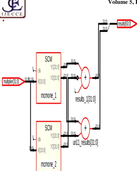
After this act, one can easily draw the circuit layout using programs such as Silicon foundry. The schematic of fig. 11 shows the gate surface of the butterfly processor. It is shown that the butterfly consists of two SCMs. The SCM is the multiplier with the 32-bit constant discriminator whose schematic is brought in fig. 11 using Simplicity program.
Copyright © 2014 IJECCE, All right reserved Fig.10. The gate surface circuit for butterfly designed by
Synplify program
Fig.11. The gate surface circuit for multiplier with 32-bit constant discriminator designed by Simplify program
By the way, it is important to note that cycle duration for write and read is much longer than other cycles in the processor. Therefore, the presence of memory banks which are designed in FFT base, can considerable improve the performance time of the processor. Nevertheless, this
strategy results in more occupation of silicon surface. The memory bank circuit on gate surface is depicted by Synplify program (fig. 12). Herein, each memory bank unit has 32-bit long. The addressing should be in an occasion in which the simultaneous write and read actions never take place. The memory has 8 address buses for read and 8 address buses for write; in other words each bank independently has address bus for write and read. In this way the address generator unit which is performed by a counter, has been made very simple and. Table 1 presents the allocation method of the memory addresses.
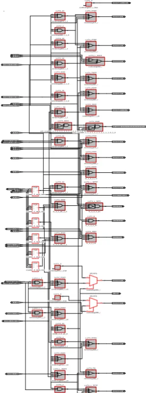
Control unit (micro coded state machine) _This unit saves all of the necessary control signals for the FFT processor operation. This unit uses a clock in order to generate the control state signals. The total number of generated states is 196 which can be generated via a counter [3]. Two signals of this unit make are supposed to connect with out of the FFT processor; the en_fft and done_fft. The en_ff signal clears all of the counters by which the states are generated so that the FFT calculation is restarted. The done-fft informs the other blocks that calculation is over and the output is ready. The gate surface circuit for control unit which is gained by simplifyprogram has been presented in fig. 13.
Fig.12. The memory bank in gate surface designed by Simplify program
Table 1: Memory mapping Ban k0 Ban k1 Ban k2 Ban k3 Ban k4 Ban k5 Ban k6 Ban k7
0 1 2 3 4 5 6 7
15 8 9 10 11 12 13 14
22 23 16 17 18 19 20 21
29 30 31 24 25 26 27 28
36 37 38 39 32 33 34 35
43 44 45 46 47 40 41 42
50 51 52 53 54 55 48 49
57 58 59 60 61 62 63 56
[31:0] [31:0]
SCM
mcmone_1
SCM
mcmone_2
un11_results[31:0]
+
results_1[31:0]
+
0 clk [31:16] X[15:0] [31:0] Y1[31:0] [31:0] Y2[31:0] 0 clk [15:0] X[15:0] [31:0] Y1[31:0] [31:0] Y2[31:0] [31:0] [31:0] [31:0] [31:0] [31:0] [31:0] 1 results[63:0] multiplier[31:0] [31:0] bc[31:2] [31:2] mcmone_2.w5[17:6] [17:6] mcmone_2.w1283[2] mcmone_2.w6415[29:3] [29:3] bc_c[1:0] [1:0] ac[31:2] [31:2] mcmone_1.w6415[29:2] [29:2]mcmone_1.w5[17:6] [17:6] ac_c[1:0] [1:0] multiplierz[24:3] [24:3] multiplier_c[31:2] [31:2] SCM mcmo ne_1 SCM_1 mcmo ne_2 MULT_AND I_793 MULT_AND I_791 MULT_AND I_789 MULT_AND I_787 INV w5_i[9] INV w5_i_0[9] INV w5_i[13] INV w5_i[14] INV w5_i[15] INV w5_i_0[13] INV w5_i_0[14] INV w5_i_0[15] INV w5_i[10] INV w5_i_0[10] LUT2_2 G_460 LUT2_2 G_576 LUT2_9 G_355 LUT2_9 G_167 LUT3_4D N_978_i 0 1 LUT3_4D N_965_i 0 1 LUT3_B2 G_51 0 1 LUT3_B2 G_239 0 1 LUT3_8E N_974_i 0 1 LUT3_8E N_975_i 0 1 LUT3_8E N_976_i 0 1 LUT3_8E N_977_i 0 1 LUT3_8E N_981_i 0 1 LUT3_B2 N_970_i 0 1 LUT3_B2 N_971_i 0 1 LUT3_8E N_961_i 0 1 LUT3_8E N_962_i 0 1 LUT3_8E N_963_i 0 1 LUT3_8E N_964_i 0 1 LUT3_8E N_968_i 0 1 LUT3_B2 N_957_i 0 1 LUT3_B2 N_958_i 0 1 LUT3_71 G_46 0 1 LUT3_71 G_234 0 1 LUT2_E N_973_i LUT2_E N_960_i LUT2_1 G_135 LUT2_1 G_323 [31]multiplier_c_13 [30]multiplier_c_12 [29]multiplier_c_11 [28]multiplier_c_10 [27]multiplier_c_9 [26]multiplier_c_8 [25]multiplier_c_7 [18]multiplier_c_0 [10]w5_i_4 [15]w5_i_9 [14]w5_i_8 [13][9]w5_i_7w5_i_3I_787_nI_789_nN_973_iN_974_iN_975_i N_976_i N_977_i N_978_i N_979 N_980 N_981_i G_167_n N_970_i N_971_i G_576_n G_135_n [24:19][1:0]multiplierz[24:19]ac_c[1:0][6] w5_0[17] w5_11[16] w5_10w5_3w5_9w5_1w5_8w5_7w5_2w5_5w5_4[7][8][10][9][15][11][13][14][29:2] w6415[29:2] [31:2] ac[31:2] [15]multiplier_c_13 [14]multiplier_c_12 [13]multiplier_c_11 [12]multiplier_c_10 [11]multiplier_c_9 [10][9][2]multiplier_c_8multiplier_c_7multiplier_c_0 [10]w5_i_4 [15]w5_i_9 [14]w5_i_8 [13][9]w5_i_7w5_i_3I_791_nI_793_nN_960_iN_961_i N_962_i N_963_i N_964_i N_965_i G_239_n G_234_n N_968_i G_355_n N_957_i N_958_i G_460_n G_323_n [8:3]multiplierz[8:3] [1:0]bc_c[1:0] [3] w6415_1[4] w6415_2[5] w6415_3[6] w6415_4[7] w6415_5[8] w6415_6[9] w6415_7[10] w6415_8[11] w6415_9[12] w6415_10[13] w6415_11[14] w6415_12[15] w6415_13[16] w6415_14[17] w6415_15[18] w6415_16[19] w6415_17[20] w6415_18[21] w6415_19[22] w6415_20[23] w6415_21[24] w6415_22[25] w6415_23[26] w6415_24[27] w6415_25[29] w6415_27[28] w6415_26w1283_0w5_11w5_10w5_8w5_2w5_3w5_4w5_5w5_7w5_1w5_0w5_9[14][15][11][16][10][17][9][8][6][7][13] [31:2] bc[31:2] I0
1I1 LO [8]1I0I1 LO
I0 1I1 LO [8]1I0I1 LO
[9]IO[9] [9]IO[9]
[13]IO[13] [14]IO[14] [15]IO[15] [13]IO[13] [14]IO[14] [15]IO[15] [10]IO[10]
[10]IO[10]
[15] [9] [15][9] [3] [13] [19] [13] [25] [27] [9] [11] [24] [26] [8] [10] [7] [29] [31] [6] [28] [30] [5] [27] [29] [4] [26] [28] [0] [22] [24] [1] [11] [17] [0] [10] [16] [7] [13] [15] [6] [12] [14] [5] [11] [13] [4] [10] [12] [0] [6] [8] [1] [11] [17] [0] [10] [16] [1] [23] [25] [1] [7] [9] [8] [30] [8] [14] [0] [1] [0] [1] read_add_c [2:0]
[2 :0 ]
write_add_c [2:0]
[2 :0 ]
write_data[31:0]
[3 1 :0 ]
memwrite_en_c read_data[31:0]
[3 1 :0 ]
c lk_c
BUFGP clk_ibuf
OBUF read_data_o buf [31]
OBUF read_data_o buf [30]
OBUF read_data_o buf [29]
OBUF read_data_o buf [28]
OBUF read_data_o buf [27]
OBUF read_data_o buf [26]
OBUF read_data_o buf [25]
OBUF read_data_o buf [24]
OBUF read_data_o buf [23]
OBUF read_data_o buf [22]
OBUF read_data_o buf [21]
OBUF read_data_o buf [20]
OBUF read_data_o buf [19]
OBUF read_data_o buf [18]
IBUF memwrite_en_ibuf IBUF write_data_ibuf [31] IBUF write_data_ibuf [30] IBUF write_data_ibuf [29] IBUF write_data_ibuf [28] IBUF write_data_ibuf [27] IBUF write_data_ibuf [26] IBUF write_data_ibuf [25] IBUF write_data_ibuf [24] IBUF write_data_ibuf [23] IBUF write_data_ibuf [22] IBUF write_data_ibuf [21] IBUF write_data_ibuf [20] IBUF write_data_ibuf [19] IBUF write_data_ibuf [18] IBUF write_add_ibuf [2] IBUF write_add_ibuf [1] IBUF write_add_ibuf [0] IBUF read_add_ibuf [2] IBUF read_add_ibuf [1] IBUF read_add_ibuf [0] RAM 16X1D memo ry.I_26 RAM 16X1D memo ry.I_25 RAM 16X1D memo ry.I_24 RAM 16X1D memo ry.I_23 RAM 16X1D memo ry.I_22 RAM 16X1D memo ry.I_21 RAM 16X1D memo ry.I_19 RAM 16X1D memo ry.I_12 RAM 16X1D memo ry.I_11 RAM 16X1D memo ry.I_10 RAM 16X1D memo ry.I_9 RAM 16X1D memo ry.I_8 RAM 16X1D memo ry.I_6 RAM 16X1D memo ry.I_3 I O
[3 1 ] I O [3 1 ] [3 0 ] I O [3 0 ] [2 9 ] I O [2 9 ] [2 8 ] I O [2 8 ] [2 7 ] I O [2 7 ] [2 6 ] I O [2 6 ] [2 5 ] I O [2 5 ] [2 4 ] I O [2 4 ] [2 3 ] I O [2 3 ] [2 2 ] I O [2 2 ] [2 1 ] I O [2 1 ] [2 0 ] I O [2 0 ] [1 9 ] I O [1 9 ] [1 8 ] I O [1 8 ]
I O
[3 1 ] I O [3 1 ] [3 0 ] I O [3 0 ] [2 9 ] I O [2 9 ] [2 8 ] I O [2 8 ]
[2 7 ] I O [2 7 ] [2 6 ] I O [2 6 ] [2 5 ] I O [2 5 ] [2 4 ] I O [2 4 ]
[2 3 ] I O [2 3 ] [2 2 ] I O [2 2 ] [2 1 ] I O [2 1 ] [2 0 ] I O [2 0 ]
[1 9 ] I O [1 9 ] [1 8 ] I O [1 8 ] [2 ] I O [2 ] [1 ] I O [1 ] [0 ] I O [0 ]
[2 ] I O [2 ] [1 ] I O [1 ] [0 ] I O [0 ]
[0 ] A0 [1 ] A1 [2 ]0 A2A3 [2 7 ][0 ][1 ][2 ]0 DDPRA0DPRA1DPRA2DPRA3W CLKW E
[2 7 ] DPO SPO
[0 ] A0 [1 ] A1 [2 ]0 A2A3 [2 0 ][0 ][1 ][2 ]0 DDPRA0DPRA1DPRA2DPRA3
W CLK W E
[2 0 ] DPO SPO
[0 ] A0 [1 ] A1 [2 ]0 A2A3 [1 9 ][0 ][1 ][2 ]0 DDPRA0DPRA1DPRA2DPRA3W CLKW E
[1 9 ] DPO SPO
[0 ] A0 [1 ] A1 [2 ]0 A2A3 [2 3 ][0 ][1 ][2 ]0 DDPRA0DPRA1DPRA2DPRA3W CLK
W E [2 3 ] DPO SPO
[0 ] A0 [1 ] A1 [2 ]0 A2A3 [2 4 ][0 ][1 ][2 ]0 DDPRA0DPRA1DPRA2DPRA3W CLKW E
[2 4 ] DPO SPO
[0 ] A0 [1 ] A1 [2 ]0 A2A3 [2 8 ][0 ][1 ][2 ]0 DDPRA0DPRA1DPRA2DPRA3W CLK
W E [2 8 ] DPO SPO
[0 ] A0 [1 ] A1 [2 ]0 A2A3 [2 5 ][0 ][1 ][2 ]0 DDPRA0DPRA1DPRA2DPRA3W CLKW E
[2 5 ] DPO SPO
[0 ] A0 [1 ] A1 [2 ]0 A2A3 [3 1 ][0 ][1 ][2 ]0 DDPRA0DPRA1DPRA2DPRA3
W CLK W E
[3 1 ] DPO SPO
[0 ] A0 [1 ] A1 [2 ]0 A2A3 [2 2 ][0 ][1 ][2 ]0 DDPRA0DPRA1DPRA2DPRA3W CLKW E
[2 2 ] DPO SPO [0 ] A0 [1 ] A1 [2 ]0 A2A3 [2 6 ][0 ][1 ][2 ]0 DDPRA0DPRA1DPRA2DPRA3W CLKW E
[2 6 ] DPO SPO
[0 ] A0 [1 ] A1 [2 ]0 A2A3 [3 0 ][0 ][1 ][2 ]0 DDPRA0DPRA1DPRA2DPRA3
W CLK W E
[3 0 ] DPO SPO
[0 ] A0 [1 ] A1 [2 ]0 A2A3 [2 1 ][0 ][1 ][2 ]0 DDPRA0DPRA1DPRA2DPRA3W CLKW E
[2 1 ] DPO SPO [0 ] A0 [1 ] A1 [2 ]0 A2A3 [2 9 ][0 ][1 ][2 ]0 DDPRA0DPRA1DPRA2DPRA3W CLK
W E [2 9 ] DPO SPO
[0 ] A0 [1 ] A1 [2 ]0 A2A3 [1 8 ][0 ][1 ][2 ]0 DDPRA0DPRA1DPRA2DPRA3W CLK
W E [1 8 ] DPO SPO
memwrite_en write_data[31:0] [3 1 :0 ]
read_data[31:0]
[3 1 :0 ]
write_add[2:0] [2 :0 ]
read_add[2:0] [2 :0 ]
Copyright © 2014 IJECCE, All right reserved Fig.13. The gate surface circuit of control unit designed by
Simplify program
IV.
M
EASURINGThe architecture was implemented by Verilog language and was simulated by Mentor Graphics’ Modelsim program. The performance got approved. The Verilog - generated signals of FFT processor is presented in fig. 14.
The memory banks should by randomly initialized in order to generate such signals. The initial and final values which are registered in memory banks are brought in tables 2 and 3.
The output digits of FFT inversely appear so it should be reformed to the original state. Also, the outputs butterflies are scaled by 0.5 to prevent the calculation-originated overflow. The calculation of 64-point FFT takes 196 cycles. The processor' clock can reach to the frequency of 40 MHz which can result in the latency about. This FFT has been rewritten by core processor [3].For calculation of the IFFT in this processor, we just need to exchange the imaginary and real values of both input and outputs [1] or to make both input and output conjugated [4].
V.
C
ONCLUSIONIn report an OFDM-based 64-point FFT/IFFT architecture for high speed WLAN systems was explored. In order to gain a less power consumption and less silicon surface, adders and shifters were employed instead of direct imaginary multiplier. Moreover, in order to decrease the processing time and to meet the IEEE 802.11 standard, 8 memory banks were used in the FFT processor. This strategy yielded the major time reduction in access to the memory. The designed FFT processor prepares the output
in 2
sec which is less than standard limit introduced inIEEE 802.11 standard [1].
Table 2: The initial values of memory banks in base 16 Bank
Address
0 1 2 3 4 5 6 7
7 12153524 80010e00 80021c00 80032a00 80043800 80054600 80065400 80076200
6 c0895e81 9c598438 b8b1fc71 d50a72aa f162e8e2 0dbb5f1b 2a13d554 466c4b8c
5 8484d609 43593986 ea58ecd4 9158a022 38585570 df5808be 8657bc0c 2d57715a
4 b1f05663 ae130c5c 18ccdf31 8386b007 ee4084dc 58fa57b1 c3b42887 2e6dfb5c
3 06b97b0d 672307ce 20330340 d942fcb2 9252f824 4b62f396 0472ef08 bd82ea7b
2 46df998d 63cc97c7 607625c0 5d1fb5ba 59c945b3 5672d3ac 531c63a6 4fc5f39f
1 b2c28465 e3132cc6 6259c1c4 e1a056c3 60e6edc1 e02d82c0 5f7419be debaaebd
0 89375212 f9d762f3 109b9921 275fcf4e 3e24057c 54e83ba9 6bac71d7 8270a604
Table 3: Thevalues of memory bank in base 16 at the end of calculation Bank
Address
0 1 2 3 4 5 6 7
7 00a0fee9 fadafedc 045100cc faf4035f f7be0128 03ed03e2 02dd0a00 ee4103d1
6 fdddf7f9 ffcdf75f fa850982 ffa8f54a fd270bcc f88b026f fc9b00d9 00fbeee3
5 fb60fdbe f697ffdf 08e4f80f 01740c13 0c9df672 050904cf fe6dfb8f fe5ef662
4 0c44f888 0036fbc8 fcfdfd40 f207feab 0249049f f7d702b1 fdfb03aa fc80fb93
3 0daefae7 0033fc55 fce50008 052cf0bb 0546fe34 0228faf4 00c30917 0a9cfe64
2 fc95f640 112f0649 fec8014f 00fe0bbc fe58fd00 09f40336 015503ab 014c00e1
1 fca0fcb9 0445f5d2 ff7c0c7a 0264f825 06f1ffbf eeebf967 fe6cfe1a 05bcf954
0 fe230743 0499fd51 03f40632 00f80466 f809044a fbf9fcda 02ddfedd 052efd98
counter_4_rep1_fast counter_0_rep1 counter_0_rep1_rep1
controlsig959_i N_1659
counter_2_rep1
counter_1_rep1 controlsig992_i controlsig958_i controlsig999_i N_1682
controlsig991_i N_1669 G_4_0_L4_n counter_7_rep1
controlsig954_6 N_1325
G_4_0_0_rn_0 G_4_0_0_sn counter_5_rep2_fast en_fft_cclk_c
counter_s[6:0] [6:0] controlsig971_i N_1393
G_4_0_2_L4_n N_1660
counter_2_rep2_fast counter_1_rep2_rep1
controlsig968_i N_1688
controlsig976_i N_1684
counter_4_rep2_rep1
un1_counter_1_1_1_1_1_1_1_1_1_1_1_0_1_0 N_1674
controlsig957_i_x1_n counter_0_rep2_rep1
controlsig965_i
N_1678 counter_3_rep2_rep1
controlsig982_i controlsig964_i N_1375
N_1374
controlsig983_i controlsig975_i
counter_fast[7:0][7:0] N_1377
controlsig957_i_true_n
LUT1_3 controlsig999_i_true
LUT1_3 controlsig991_i_true
LUT1_3 controlsig957_i_true
LUT4_FFBF
controlsig975_i
LUT4_FFBF
controlsig983_i LUT2_2
controlsig983_i_1_0
LUT4_L_EFFF
controlsig964_i LUT4_FBFF
controlsig982_i LUT4_0002
controlsig982_i_1_0 LUT4_FDFF
controlsig965_i LUT3_7F
controlsig965_i_1_0 LUT4_7FFF
controlsig957_i_x1 LUT4_0045
un1_counter_1_1_1_1_1_1_1_1_1_1_1_0_1_0 LUT4_5554
un1_counter_1_1_1_1_1_1_1_1_1_1_1_0_1_0_sx LUT3_02
controlsig964_i_1
LUT4_F7FF
controlsig976_i LUT4_F7FF
controlsig968_i LUT3_02
controlsig968_i_1
LUT4_FDFF
G_4_0_2_L4 LUT4_L_BFFF
controlsig971_i LUT3_20
controlsig971_i_1 LUT3_10
controlsig975_i_1
LUT3_20
controlsig983_i_1
FDR counter_6_rep2_fast
FDR counter_5_rep2_fast
FDR counter_4_rep2_fast
FDR counter_3_rep2_fast
FDR counter_1_rep2_fast
FDR counter_0_rep2_fast
LUT4_L_0070
G_4_0_0_sn LUT2_8
G_4_0_0_rn LUT4_4000
G_4_0_L4
MUXF5
controlsig991_i LUT4_FDFF
controlsig991_i_x1 MUXF5
controlsig999_i LUT4_FDFF
controlsig999_i_x1
LUT4_FFFD
controlsig958_i
LUT3_FD
controlsig992_i LUT4_L_FDFF
controlsig992_i_sx LUT4_FEFF
controlsig958_i_sx
LUT4_L_FF7F
controlsig959_i LUT2_2
controlsig959_i_1 LUT2_L_2
controlsig999_i_1 LUT2_L_2
controlsig991_i_1 LUT3_L_04
controlsig957_i_1
LUT2_2
controlsig958_i_1 LUT4_0800
G_4_0_a6_1_5
LUT4_0010
G_4_0_a6_1_4
LUT3_40
m295_0_0_a2_6
0 0
0 [2]
[2] [0] [1]
[7] [2] [7] [0] [1] [6]
[6] [7] [1] [2]
[1] [2] [7] [0] [1] [2] [0] [6]
[6] [7]
[6] [7] [0]
[6] [7] [0] [6] [7] [6] [7]
[6] [7]
[6]
D C RQ
[5]
D C RQ
[4]
D C RQ
[3]
D C RQ
[1]
D C RQ
[0]
D C RQ
I0 I1 S
O
[2] [6] [7]
I0 I1 S
O
[2] [6] [7]
[3] [5]
[0] [6] [7] [0] [1] [2] [7]
[2] [1] [1] [1]
[0] [6]
Copyright © 2014 IJECCE, All right reserved Fig.14. The generated signals simulated by Mentor
Graphics’ Modelsim software
R
EFERENCES[1] K. Maharatna, E. Grass, U. Jagdhold, “A 64-point Fourier transform chip for high-speed wireless LAN application using OFDM”, IEEE J. Solid-State Circuits, vol. 39, pp. 484-493, Mar. 2004
[2] B. M. Baas, “An approach to low-power, high-performance, fast Fourier transform processor design,” Dissertation, Stanford University, Stanford, CA, 1999.
[3] Arish Alreja, "Real Time OFDM engine for High Speed Wireless Applications", GEORGIA INSTITUTE OF TECHNOLOGY, ECE 4902.
[4] Yuan Chen; Yu-Wei Lin, Chen-Yi Lee, "A Block Scaling FFT/IFFT Processor for WiMAX Applications, " Solid-State Circuits Conference, 2006. ASSCC 2006. IEEE Asian , vol., no., pp.203-206, 13-15 Nov. 2006.
[5] J. C. Candy and G. C. Temes, “Oversampling Delta-Sigma Data
Converters,” Piscataway, NJ: IEEEPress, 1992, ISBN
0-87942-285-8
[6] S. R. Northworthy, R. Schreier, and G. C. Temes, “Delta-Sigma Data Converters,” Piscataway, NJ: IEEE Press, 1997, ISBN 0-7803-1045-4
[7] Mohammad Yavari and OmidShoaei,”A 3.3V Second-Order
Sigma-Delta Modulator for Digital Audio,” Electrical &
Computer Engineering Department, University of Tehran, Iran [8] ShahriarRabii and Bruce A. Wooley,”A 1.8-V Digital-Audio
Sigma-Delta Modulatorin 0.8-m CMOS,” Stanford
University.Stanford, CA 94305
[9] SumithkumarNathany ,”14- bit Fully differential discrete time sigma-delta modulator,”A Thesis for the Degree of master of science Department Of Electrical Engineering KATE GLEASON College Of Engineering. Rochester Institute Of Technology .ROCHESTER, NEW YORKNOVEMBER 2006 [10] brianP.Brandt, drew E.Wingard ,Bruce A.Wooley ,”Second
Order Sigma-Delta Modulation For Digital-Audio Signal
Acquisition,” IEEE JOURNAL OF SOLID STATE CIRCUITS
![Fig.7. Data path in FFT processor [3].](https://thumb-us.123doks.com/thumbv2/123dok_us/8787470.1764734/3.595.59.286.361.739/fig-data-path-fft-processor.webp)