Conversion For Wireless Sensor Node
[1]
Donia Maria Denny, [2]K.Indumathi, [3]Dr.S.Radha, [4]T.S.Shri Krishnan, [5]Jemimah Ebenezer, [6]R.Jehadeesan [1] [2] [3]
Electronics and Communication, SSN College of Engineering, Kalavakkam, [4] [5] [6]
Computer Division,Indira Gandhi Centre for Atomic Research, Kalpakkam.
Abstract
:
In future reactors, WSN is going to take a major role in the monitoring and control instrumentation. Diversity and redundancy are the prime requirements of nuclear domain. To provide diversity in the data acquisition method of WSN, instead of using legacy ADCs, an alternate method of digitization can be introduced. This paper proposes a method of digitizing using the concept of Voltage to Frequency Conversion (VFC). But there exists a serious constraint on resources like energy, memory and bandwidth for a deployment based on wireless sensor nodes. Key idea explained in this paper is about the selection of components, which consumes minimum energy, to develop a signal conditioning board that performs signal digitization utilising VFC. This paper also explains the establishment of a typical network that utilizes VFC.Keywords:Wireless Sensor Network, Voltage to Frequency Conversion, VFC, Signal digitization, Data acquisition.
I. INTRODUCTION
Wireless Sensor Network (WSN) is a network of many sensor nodes which are employed for sensing various physical parameters. These sensed data are transmitted wirelessly to the receiving end; generally called as base station. Wireless sensor node consists of many blocks such as power supply block, microcontroller, transceiver, sensors, signal conditioning board and Analog to Digital Converter (ADC) as shown in Fig. 1.
Fig.1 Wireless Sensor Node Architecture
Power Supply block is the main source that provides power to the WSN node. It is designed to meet the power requirement of the node. Power consumption is more during the sensing of process parameters, processing of sensed data and during the transmission of the processed data. Reduction of energy consumption is an important task to be followed because these sensor nodes are deployed in sites where availability of power source is limited. Microcontroller is used for processing the sensed data and to handle the RF protocol stack.Processed data is transmitted via a transceiver utilizing radio frequency to the base station where the data can be viewed.
The conditioned signal is then digitized by an ADC. Sample & hold circuitry of ADC samples the input and converts an analog signal to a discrete time and discrete amplitude digital signal. ADC generates a digital number proportional to the magnitude of the input analog voltage. This conversion involves quantization of the input so that, only a small amount of error is introduced.
In general ADCs are the primary mode of digitization. In order to have a better resolution, dynamic ranging than the available traditional ADCs and to have an alternate method of digitizing, concept of Voltage to Frequency Conversion (VFC) is presented in this paper. A typical application of acquiring slow varying signal like thermocouple is also explained.
II. VOLTAGE TO FREQUENCY CONVERTER
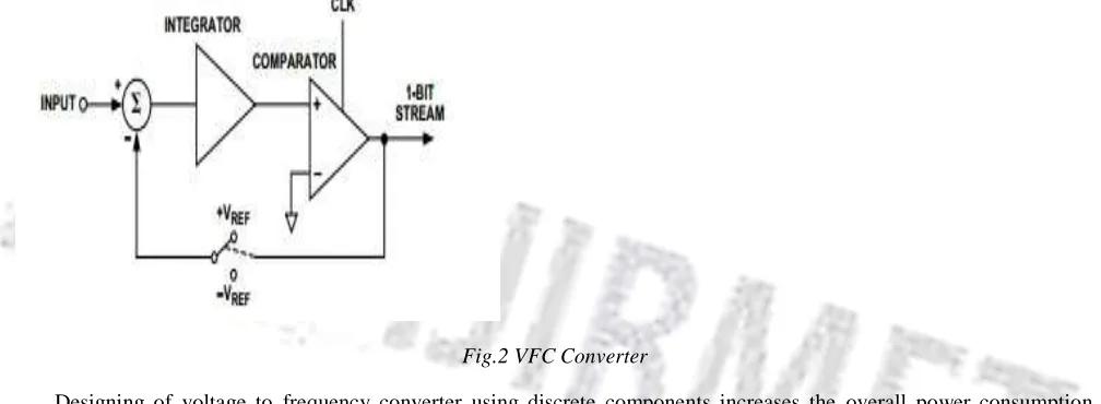
VFC generates a stream of pulses with frequency proportional to the input voltage. VFC works on the principle of current integration and comparison with input voltage as shown in Fig.2 [3]. In the first stage of VFC, input voltage is passed through an integrator that produces a ramp signal and this signal is compared with a comparator that produces a
negative or positive voltage. The output voltage from the comparator is again given as a feed-back to integrator which gives a triangular wave as output. Slope of the triangular wave and ramp signal is proportional to the input voltage. Integrator output is compared with a reference signal in the comparator to produce a pulse signal.
Fig.2 VFC Converter
Designing of voltage to frequency converter using discrete components increases the overall power consumption. Since, discrete components individually contributes to increase in overall power consumption, a single VFC IC provides a better solution to this problem.
TABLE 1: Comparison of VFC converters based on specifications
Parameters ADVFC32
[4]
VFC32 [5]
AD7741 [6]
Voltage 10 V 22 V 5V
Input current 10mA 6 mA 8 mA
Internal Non- linearity
0.2%(at 500 KHz)
0.01%(at 10KHz)
0.012%(at 1.35MHz)
Max output frequency
The VFC is selected based on comparison among different venders as shown in Table 1. It has single channel converter which consumes typically 6 mA current and also has a power down feature that reduces the current consumption to less than 35 µA. Moreover it has very less gain error, thus AD7741 is chosen to perform VFC.
III. TYPICAL APPLICATION
In this paper a typical application of acquiring a slow varying signal from thermocouple is used as input. Design has been made with a provision to connect eight thermocouple signals.
A. Hardware Development
Signal conditioning board to acquire eight thermocouple inputs consists of blocks as shown in Fig.3. Thermocouple leads are connected to an 8x1 multiplexer since the VFC chosen is for a single channel. Selected input will be fed to an instrumentation amplifier which conditions the signal to get digitized using the VFC IC. The frequency output is given to a counter to count the pulses. Final count corresponding to the input voltage is read by the microcontroller. The host microcontroller in the main board is connected to a pre-configured RF233 based zigbee module which transmits the thermocouple data to the base station where data corresponding to individual channel can be viewed in a Graphical User Interface (GUI).
Fig. 3 Block diagram of proposed model
B. Component Selection
Multiplexer: Multiplexer is termed as a data selector due to the fact that it selects one of many analog or digital inputs. The selected input is then forwarded onto a single channel thus facilitating many signals to share a single common medium.
Different multiplexers are compared as shown in Table 2. Based on the specification of minimum current consumption and operating voltage, ADG707 has been selected. This analog multiplexer is capable of handling 16 single channels or eight differential channels.
The ADG707 Multiplexer switches between one of eight differential pairs of thermocouple input. The selected signal is then forwarded to a common differential output as determined by the 3-bit binary address lines. Address lines A0, A1, and A2are connected to the GPIO pins of the microcontroller. An EN pin is used to enable or disable the multiplexer.
TABLE 2: Comparison of multiplexers based on specifications
Parameters 74HC151
[7]
74HC153 [8]
ADG707 [9]
Voltage 7V 7 V 5.5 V
Power Consumption
500mW 500mW <0.01µW Leakage current ±0.1µA
(25ºC)
±0.1µA (25ºC)
Differential channels
8x1 4x1 8x1
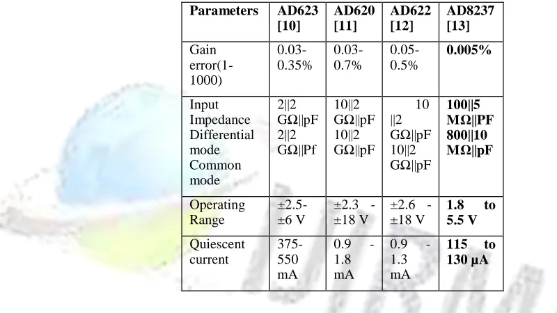
Instrumentation Amplifier: Instrumentation amplifier has high input impedance due to which it does not load the input system. Hence this amplifier is aptly suitable for use in industrial data acquisition. Instrumentation amplifiers provide better accuracy and stability.
AD8237 is chosen as the instrumentation amplifier because it provides very less gain error and very high input impedance. Moreover it operates right from 1.8V and current consumption is far less than other amplifiers. Gain is set by using two external resistors and it creates low gain drift at all gains.
TABLE 3: Comparison of Instrumentation Amplifiers based on specifications
Parameters AD623 [10] AD620 [11] AD622 [12] AD8237 [13] Gain error(1- 1000) 0.03- 0.35% 0.03- 0.7% 0.05- 0.5% 0.005% Input Impedance Differential mode Common mode 2||2 GΩ||pF 2||2 GΩ||Pf 10||2 GΩ||pF 10||2 GΩ||pF 10 ||2 GΩ||pF 10||2 GΩ||pF 100||5 MΩ||PF 800||10 MΩ||pF Operating Range ±2.5- ±6 V
±2.3 - ±18 V
±2.6 - ±18 V
1.8 to
5.5 V Quiescent current 375- 550 mA
0.9 - 1.8 mA
0.9 - 1.3 mA
115 to
130 µA
Counters: Counters are used to count the number of pulses from the VFC. Upon comparison of various counters,
SN74LV8154 is a 32-bit counter which can also be used as a dual 16-bit counter is chosen. It provides 8 bit data lines where individual lines are configured as 3 state logic output. To map a 32-bit storage register on the 8 bit output bus, four bus reads are required. The GAL, GAU,
GBL, GBU inputs are used to select the byte that needs to be output at Y0−Y7. These select lines are configured as GPIO output while data bus lines are set as input in microcontroller.
TABLE 4: Comparison of Counters based on specifications
Parameters HEF45 16B [14] 74HC1 93 [15] MC145 16B [16] SN74L V8154 [17]
Voltage 18 V 7 V 8 V 7 V
Supply Current
50 mA 50mA 10mA 20µA
Power Dissipation
100 mA 500 mW
500 mW
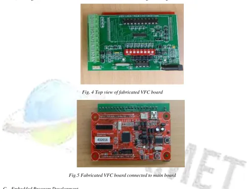
After careful selection of individual components, signal conditioning board which does digitizing using the concept of VFC, is designed and fabricated. Fabricated VFC board is shown in Fig.4 and Fig.5
Fig. 4 Top view of fabricated VFC board
Fig.5 Fabricated VFC board connected to main board
C. Embedded Program Development
Embedded program involves usage of primitive APIs and development of drivers to interface GPIOs and SPI. GPIO pins are used to control the select lines of multiplexer and counter. SPI is used to interface pre- configured RF233 based zigbee module. APIs are used for communicating with the transceiver.
1) General Purpose Input/Output (GPIO)
GPIO is an interface available on microcontrollers to provide an ease of access to the device internal properties. GPIO pins on a single microcontroller can be programmed as input or Output and can be pulled-up or pulled-down. Address lines A0, A1 and A2 of multiplexer are connected to GPIO pins that are configured as output in the microcontroller. Similarly, data lines Y0-Y7 of counter are interfaced with input pins and the control address lines are interfaced with output pins, by configuring the GPIO pins of the host microcontroller.
2) Serial Peripheral Interface (SPI)
high) or falling (high to low) edge of the clock signal. When the receiver detects that corresponding edge, it will immediately read the data line. Flowchart of SPI communication is explained in Fig. 6.
Fig. 6 Flowchart for SPI driver
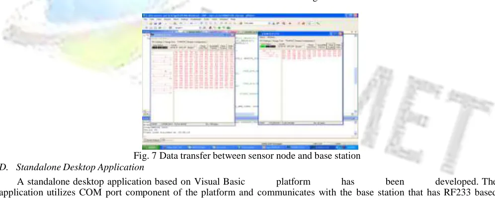
Sensor node is interfaced with pre-configured RF233 based transceiver module using SPI. Transceiver is programmed with a minimalistic Zigbee RF stack. APIs are used for communication between transceiver module and the microcontroller of sensor node. Data transfer between sensor node and base station is shown in Fig. 7.
Fig. 7 Data transfer between sensor node and base station
D. Standalone Desktop Application
A standalone desktop application based on Visual Basic platform has been developed. The application utilizes COM port component of the platform and communicates with the base station that has RF233 based transceiver. The application then parses the content of the frame being received through the COM port and displays the readings of the sensor node in its corresponding textbox. Database connectivity using MS Access has been provided to log the temperature readings.
Fig.8 Display of Thermocouple readings at base station
IV. CONCLUSIONS
Generally all the sensor nodes will be using ADCs to digitize the real world analog data. But in a field where diverse and alternate mode of digitizing is required, solution based on Voltage to Frequency can be utilized. To check the functionality based on this digitization, a typical application has been identified to connect 8 thermocouples and a suitable VFC hardware has been designed. In this paper, the flow involved in the development of digitization, circuit fabrication, embedded program development to read the process parameter and finally displaying the thermocouple readings in a standalone application are explained.
V. REFERENCES
[1] Azcona, B. Calvo, N. Medrano, S. Celma, “Voltage-to-Frequency Converter for Low-Power Sensor Interfaces”, SENSORS, 2011 IEEE
[2] B.Calvo, N.Medrano, S.Celma “A Full-Scale CMOS Voltage-to-Frequency Converter for WSN Signal Conditioning”, Circuits and Systems (ISCAS), August 2010
[3] Behera, J. R., & Barik, R. K. (2012). “Voltage to Frequency Converter: Modeling and Design (Doctoral dissertation)”.
[4] The datasheet of, “ADVFC32 Voltage-to-Frequency and Frequency-to-Voltage Converter”, Available at: http://www.analog.com/media/en/technical- documentation/data-sheets/ADVFC32.pdf
[5] The datasheet of, “Voltage-to-Frequency and Frequency-to-Voltage converter, VFC32”, Available at: http://www.ti.com/lit/ds/sbvs015/sbvs015.pdf
[6] The datasheet of “Single and Multichannel, Synchronous Voltage-to-Frequency
Converters AD7741”, Available at:http://www.analog.com/media/en/technical- documentation/data-sheets/AD7741_7742.pdf
[7] The datasheet of, “74HC/HCT151 8-input multiplexer”, Available at: http://lbk.fe.uni-lj.si/pdfs/PV-IC- datasheet/74HC151.pdf
[8] The datasheet of, “74HC/HCT153 Dual 4-input multiplexer”, Available at: http://www.futurlec.com/74HC/74HC153.shtml
[9] The datasheet of, “CMOS, +1.8 V to +5.5 V/2.5 V, 2.5 Low-Voltage, 8-/16-Channel Multiplexers ADG707”,Available
at:http://www.analog.com/media/en/technicaldocume ntation/datasheets/ADG706_707.pdf
[10] The datasheet of, “Single and Dual-Supply, Rail-to- Rail,Low Cost Instrumentation Amplifier”, Available at: http://www.analog.com/media/en/technical- documentation/data-sheets/AD623.pdf
[11] The datasheet of, “Low Cost Low Power Instrumentation Amplifier AD620”, Available at:
[12] The datasheet of, “Low Cost Instrumentation Amplifier AD622”, Available at :
https://lib.chipdip.ru/143/DOC000143648.pdf
[13] The datasheet of “Micropower, Zero Drift, True Rail- to-Rail Instrumentation Amplifier”, Available at: http://www.analog.com/media/en/technical- documentation/datasheets/AD8237.pdf
[14] The datasheet of,” HEF4516B MSI Binary up/down counter, Available at:
http://html.alldatasheet.com/html- pdf/17749/PHILIPS/HEF4516B/247/1/HEF4516B.ht ml
[15] The datasheet of, “74HCT193-Q100 Presettable synchronous 4-bit binary up/down counter”, Available at: http://assets.nexperia.com/documents/data- sheet/74HC_HCT193_Q100.pdf
[16] The datasheet of, “MC14516B Binary Up/Down Counter”, Available at: https://www.onsemi.com/pub/Collateral/MC14516B- D.PDF