Low Power and Area Efficient Carry Save Adder
Based on Static 125nm CMOS Technology
D. Hema B. Indhumathi
BE Student BE Student
Department of Electronics & Communication Engineering Department of Electronics & Communication Engineering SNS College of Technology, Coimbatore - 35 SNS College of Technology, Coimbatore - 35
M. Ishwarya G. Hemanth Kumar
BE Student BE Student
Department of Electronics & Communication Engineering Department of Electronics & Communication Engineering SNS College of Technology, Coimbatore - 35 SNS College of Technology, Coimbatore - 35
G. Naveen Balaji
Assistant Professor
Department of Electronics & Communication Engineering SNS College of Technology, Coimbatore - 35
Abstract
In a digital circuit theory combinational logic is a type of the digital logic implemented by Boolean circuits where the output is dependent of pure present input. A Carry save adder is one of the type of the digital adder that is used in the computer micro architecture to compute the sum of the three or more n-bit binary numbers in binary. It differs from other digital adders in that it outputs two numbers of the same dimension as the inputs one which is a sequence of partial sum bits and another which is a sequence of partial sum bits and another which is a sequence of carry bits. It has few advantages such as it produces all of its outputs in parallel resulting in the same delay as full adder. It has very little propagation delay when implemented. Carry Save adder plus ripple adder is equals to n+1. Two ripple carry adders is equals to 2n. It allows for high clock speeds. Though it is some advantages it also has some disadvantages such as we do not know whether the result is positive a negative. While performing modular multiplication. The behaviour of the efficient Carry Save Adder is designed using tanner eda tools which was useful and the currently existing carry skip adder is designed using xilnx software and lastly the layout for this research is designed with the help of multisim. With help of this research many newly created circuits can designed much smaller.
Keywords: carry save adder, CMOS, static CMOS, 125nm, tanner, multisim, Xilinx, half adder, Full adder, Ripple carry adder
_______________________________________________________________________________________________________
I. INTRODUCTION
A combinational circuit is said to be a circuit in which the output is depend upon the function given by the input which is implemented by various Boolean expression according to the connection given to each gate ,though this may be considered controversial such as half adder, full adder, half subtractor, full subtractor , multiplexer, demultiplexer, encoder and decoder are also shared its classification under combinational logic A carry save adder [1][2][nb1] is a type of digital adder used in computer micro architecture to compute the sum of three or more n-bit numbers in binary it differs from other digital adders in that it outputs two numbers of the same dimensions as the inputs, one which is asequence of partial sum bits and another which is a sequence of carry bits . It can do multiplication of two unsigned binary numbers. Each bit o the multiplier is multiplied against the multiplicand, the product is aligned according to the position of the bit within the multiplier and the resulting products are then combined to form the final result. It is has some applications such as the fastest adders are carry save adders with the penalty of area, the simplest adder topologies that are suitable for low power applications are ripple carry adder, Carry skip and carry bypass adders with gate count and maximum delay. This research paper is for designing a carry skip adder in 125nm static technology
II. EXISTING SYSTEM
gates which performs very basic operations according to the connections made in the CMOS (Complementary Metal Oxide Semiconductor
Gates used in the Carry Skip Adder are ‘xor’ gate, ‘and’ gate, ‘not’ gate. Generally gate are the building blocks of the the combinational circuits .Gates are built using several numbers of transistor. We know that Moore’s law which states every six months number of the transistors used in a particular integrated circuit will be increased due to the technology enhancement. The XOR gate is a combinational logic gate that gives a ‘1’ output when the number of ‘1’ inputs is odd. An XOR gate implements an exclusive or, that is, a ‘1’ output results if one, and only one, of the inputs to the gate is ‘1’. If both inputs are ‘0’ or both are ‘1’, a ‘0’ output results. In ‘and’ gate ,only multiplication operation can be done if the both input are same the output will be the same as the input and if the inputs are different then the output will ‘0’. In ‘not’ gate, contains only one input and the output is the output of the input if the input is ‘1’ then the output will be ‘0’ vice versa
Fig. 1.1: Block diagram of Half Adder
In Fig 1.1 we can analyze that a half Adder consist of two inputs ‘a’ and ‘b’ and output ‘sum’and ‘carry’. Carry Skip Adder is buildup of multiple full adders and full adders are made with two half adder A truth table is a logically based mathematical table that expatiates the conceivable sequels of scenario the truth table suppresses the truth values thar would appear under the premises of the given scenario. The rows of a basic truth table contain the Boolean logic true or false values while the columns list the premises of a scenario as well as conclusion.
Fig.1.2: Logic diagram of Half Adder
In fig 1.2 Gates like ‘xor’, ‘not’, and ‘and’ Gates which are used to process the inputs and give the output. Each gate has a difference type of process algorithm based the connection given to the CMOS. The Boolean expression of the half Adder is as follows
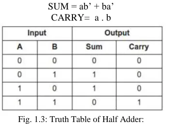
SUM = ab’ + ba’ CARRY= a . b
Fig. 1.3: Truth Table of Half Adder:
In Fig 1.3 is a truth table of the half Adder which portrays the output of that logical circuit. A half Adder is a basic arithmetic processor which perform only subtraction its only function is to deduce a single bit binary from the input
III. CARRY SAVE ADDER
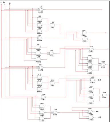
Fig. 2.1: Block diagram of Carry Save Adder:
In Fig2.1 we can analyze that a Carry Skip Adder consist of two inputs ‘a0’, ‘b0’, ‘c0’, ‘a1’, ‘b1’, ‘a2’, ‘b2’, ‘a3’ and ‘b3 whereas output ‘sum’and ‘carry’
In Fig 2.2 When the inputs are given through the respective labels gates present the circuits will process the data and perform the arithmetic operation subtraction and produce the Respective output sum and carry.
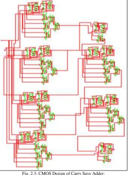
Fig. 2.3: CMOS Design of Carry Save Adder:
In Fig 2.3The above Carry Save Adder is designed using static cmos algorithm under 125 nm which is quite efficient and the results are same as the currently existing one When the inputs are given through the respective labels gates present the circuits will process the data and perform the arithmetic operation subtraction and produce the Respective output sum and carry
IV. RESULTS
Output
Waveform of CMOS design of Carry Save Adder:
V. CONCLUSION
It has been observed from the simulation results that performance of adder architectures varies with various CMOS design. The output of these two designs of Carry Save Adder are same. The current fabrication size of Carry Save adder is 125nm.If the fabrication size reduced to less than 100nm, the adder performance varies and can be absorbed using static (CMOS) technology. From this research the (CMOS) can be achieved by operating point within 0.9v.This research is very useful and more advantageous in future microprocessor industries.
REFERENCES
[1] N.Weste and K.Eshraghian,--Principles of VLSI Design, A system perspective, Reading, MA: Addison-Wesley,1993.
[2] Shital Baghel, Pranay Kumar Rahi,Nishant Yadav,2015,”(CMOS) Half Adder Design & Simulation Using Different Foundry”, International al Journal
of Innovative Science, Engineering & Technology(IJISET),Vol.2 Issue 3,pp.195-622,Aug.2000.
[3] Ming-Bo Lin, “Introduction to VLSI systems A logic, circuit and system perspective,” Taylor & Fransis group,ch. 7
[4] Neil H.E.Weste,DavidHarris and Ayan Banaerjee,”CMOS VLSI Design”.Pearson Education,Inc.,pp.11,Third edition,2005.
[5] M. Morris Mano, Michael D. Cilleti “Digital Design”,4th edition,pp.143,2012.
[6] Kaushik Roy and S.C.Prasad,”Low power CMOS VLSI circuit design”,Willey,pp.1-129,2000
[7] E.M.M.Poncino,(1996)Power Consumption of Static and Dynamic CMOS circuits, IEEE,2nd International Conference on ASIC,pp.425-427.
[8] P.S.Aswale and S.S.Chopade,(2013) Comparative Study of Different Low Power Design Techniques for reduction of Leakage power in CMOS VLSI
Circuits,IJCA(0975-8887,Volume 70-NO.1
[9] R.L.Geiger, P.E.Allen, N.R.Strander(2013) VLSI Design techniques for Analog and Digital Circuits, McGraw Hill,New Delhi, India,.[page.No.597-ch7
[10] S. Shobana, R. Ramya, K.K. Rashika, G. Naveen Balaji, K. Boopathiraja, “Hamming Window Function based FFT Analysis of Advanced Approximate
Adder design in 125nm CMOS technology using Transmission gates”, International Journal of Science and Innovative Engineering & Technology, Vol. 5, Issue: May 2018.
[11] G.NaveenBalaji,P.Malini,T.Poovika, P.Shanmugavadivu, “14T Full Adder in 125nm CMOS technology for FFT applications using piecewise constant