5
International Journal of Engineering and Management Research, Vol. 2, Issue-4, August 2012
ISSN No.: 2250-0758
Pages: 5-10
www.ijemr.net
Mobility Degradation and Total Series Resistance of Cylindrical
Gate-All-Around Silicon Nanowire Field-Effect Transistor
Lalit Singh1, Mahesh Chandra2 and B P Tyagi
1, Physics Department, Graphic Era Hill University, Bhimtal Campus, UK, India.
3
2 and 3, D B S (PG) College, Dehradun, 248001, Uttarakhand, India
,
ABSTRACT
Multi gate Si-based devices such as tri-gate or gate-all-around (GAA) nanowire (NW) Metal Oxide Semiconductor Field Effect Transistors (MOSFETs) are promising candidates for aggressively scaled CMOS due to their excellent electrostatics control. However, the carrier velocity i.e. mobility of carriers in these devices is generally degraded due to quantum–mechanical confinement effects. In this paper, the mobility-degradation factor and the series resistance of cylindrical gate-all-around silicon nanowire field-effect transistor (SNWFET) is discussed using the same mobility degradation model as in the case of conventional MOSFET. The calculation is done by defining voltage as a function of the saturation drain current evaluated from devices with various dimensions. The calculated mobility-degradation factor is an order of magnitude larger than those of other conventional MOSFET. This exhibit the more possibility of interfaces scattering in the strong inversion condition, while the gate of presented model turn off the electron channel. The calculated series resistance is mostly due to the crowding of the electron flow along the sidewall of the n+ contact.
Key words -Mobility Degradation Factor, Nanowire, Series Resistance, Gate-All-Around (GAA) Silicon Nanowire Metal Oxide Semiconductor Field Effect Transistor (SNW-MOSFET).
I INTRODUCTION
Current nano electronics technology pushes device dimensions toward the limits where the traditional semi classical theory can no longer be applied [12]. A total quantum mechanical approach which can describe the quantum-transport in nanostructures is therefore required. Recently reported device structures such as metal-oxide
semiconductor (MOS) have channel length of the order of 10 nm or even smaller. Computational studies can help address these issues, but the method commonly used in computer- aided design tools does not include important quantum mechanical effects. What is really needed is a full quantum transport model that describes quantum phenomena (especially confinement and tunnelling) as well as phase randomized scattering. Computational efficiency is necessary to permit use for engineering design and to explore numerous design options. It would be useful for such a program to be based on an approach that can be extended to nonconventional devices, such as Double Gate (DG) MOSFETs, Tri Gate (TG) MOSFETs, Gate–All-Around (GAA) silicon nanowire (SNW) MOSFETs and other molecular transistors. Among these, GAA SNWFETs [1, 2] are important candidates for sub-50-nm VLSI technologies, since their gate structure is expected to be the most efficient among 3-D devices. In particular, this structure with circular cross sections are more interesting, since they do not have corner effects and their characteristics can be modelled by an analytic formula obtained by solving the Poisson/drift-diffusion equation in the cylindrical coordinate [4] [11]. However, most of the studies on this device have yet been based on the constant mobility model [4]. Here, we address the mobility degradation and the series resistance of this model due to the gate electric field.
II MODEL
6
Radial direction
R
Silicon
Oxide
Gate
VD VS
Intrinsic Silicon 2R
S D
VG
VG
to
Gate
S
D
SiNW Channel Oxide layer
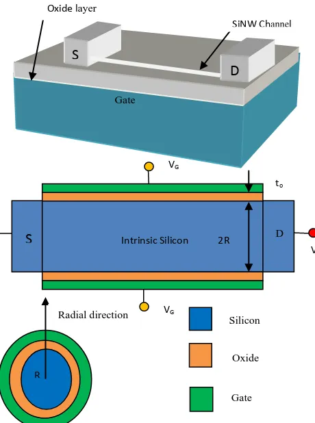
Figure (1)- Ideal GAA SiNW MOSFET: Cross sections along source to Drain and along Radial direction.
III SCATTERING MECHANISM
It is the dominant factor in planer MOSFET. Its value can be determined by several mechanisms. Here the major scattering
Mechanisms that affect a MOSFET’s inversion layer carrier mobility are:
(i) Phonon scattering due to lattice vibrations;
(ii) Surface roughness scattering due to the microscopic roughness of the Si–SiO2 interface;
(iii) Columbic scattering from ionized bulk impurities; and
(iv) Columbic scattering from the Si–SiO2 interface charges
Now in this next section. We will discuss each mechanism separately.
III (A) PHONON SCATTERING LIMITED
MOBILITY (µh)-
Such type of scattering mechanism dominates at high temperature because the lattice vibrates more violently. The temperature and transverse electric field dependence of µph is found to be µph αT-3/2Eeff-1/3.
III (B) SURFACE ROUGHNESS SCATTERING LIMITED MOBILITY (µ
.
SR)-
Surface roughness scattering is important under strong electric field in the channel (Eeff) because a stronger Eeff
True microscopic interface based calculation does not exist. Instead, a semiclassical relationship pulls inversion electrons closer to the interface. So far a
( )
211 .
eff eff SR
E
E α
µ is widely accepted. The temperature
dependence µSR has been controversial. The argument that µSR is independent of temperature is mainly based on the fact that when Eeff is large, the measured electron mobility, Eeff , stays almost constant with temperature. Since µSR dominates in this large Eeff regime, constant mobility µeff (T) is interpreted to mean that µSR is independent of T. This argument could be misleading because another mechanism, phonon scattering, also dominates in this
Region the data obtained at high T and high Eeff are the combined effect of both phonon and surface roughness scattering. Actually a higher temperature gives electrons more kinetic energy and makes them less vulnerable to surface roughness scattering. Based on such understanding, the expression for µSR (T, Eeff
(
,)
1/ −2.1eff eff
SRT E αT αE
µ
) is given
Where α is a small positive number, which is nearly equal to 2.
III (C) BULK CHARGE COLUMBIC SCATTERING LIMITED MOBILITY
(µcb
At low temperature, this mechanism exists because slower electrons are more susceptible to Columbic scattering. It depends linearly on temperature .And the effective field dependence of µ
)-
cb is explained by screening effect. A
larger Eeff
(
)
2eff eff cbT E αT E
µ ,
causes a larger electron density in the channel. This shields the Coulombic potential of impurity centres exerted on each individual electron, resulting in a decreased Coulombic scattering rate or increased electron mobility.
Therefore
However, at high temperature such type of mechanism is not important because of the high thermal velocity of charge carriers (electrons). Therefore, the interaction time between the fast moving carriers and the ionized impurity centres is short; hence the scattering probability is low.
III (D) INTERFACE CHARGE COULOMBIC SCATTERING LIMITED MOBILITY, µint (T, Eeff
Two competing processes occur for the Coulombic scattering of interface charges. When the temperature is decreased, the electron thermal velocity is reduced so that the Coulombic scattering rate by interface charges should be larger, as happens for bulk impurity scattering. However, a reduced temperature also results in a reduced ‘screening’ effect. It is believed that the screening effect dominates the two competing processes for the interface charges. Thus Increasing E
)-
eff also causes two competing
processes for interface Coulombic scattering. One is that an increased Eeff gives rise to denser channel electrons
7
scattering term has a similar Eeff dependence as µcb. But it
is weakened by the competing process mentioned above. Thus µint is linearly dependent on Eeff , rather than the
stronger square dependence of Eeff in µcb . The following
µint(T, Eeff
(
T Eeff)
αT−1Eeffµint ,
)expression is then proposed:
Based on the above discussion, the expression for the effective mobility can be calculated by Mathiessens formula. But here we are considering the mobility degradation factor for GAA structure mainly due to interface scattering.
IV
EXPRESSION FOR EFFECTIVE
MOBILITY
Several models, for surface mobility, have been discussed in the literature. In most of the cases, the mobility is described as a function of transverse electric field. The effective carrier mobility is expressed as [11],
γ
µ
µ
+
=
01
E
E
z oeff ,
where
µ
o is the carrier mobility at z = 0 means at the surface. Now, using Gauss theorem, we can write electric field intensity in terms of charge densities. thereby
+
+
=
γβ
ε
µ
µ
S B o Si o effQ
Q
E
1
1
(1)Where, the terms
ε
Si,
Q
S,Q
B, Cox,
2
ε
SiC
Oxα
θ
=
θand ϴ
( ) are permittivity of Si, mobile charge,
depleted charge per unit area , Oxide capacitance and mobility degradation factor respectively.
µ
o,a
θ,γ
, andβ
depend on temperature. These are taken to be the fitting parameters. For the Gate – All - Around (GAA) transistor the transverse electric field at the gate is radial. So whenγ
=1, the transverse electric field (Er) has a similar effect on μeff as Ez(
GS oT)
B SBeff
V
V
V
θ
θ
µ
µ
+
−
+
=1
does on conventional planer MOSFETs. The effective carrier mobility is, therefore, expressed as [10]
(
V
GSO−
V
T)
+
≈
θ
µ
1
(2)The mobility-degradation factor is
β
ε
θ
o Si OxE
C
=
And the Oxide capacitance is
+
=
R
t
R
C
Ox Ox Ox1
ln
ε
V EXPRESSION FOR DRAIN CURRENT
The expression for the drain current (IDS
(
)
C(
V V( )
T)
L W E T
I Ox GS T
eff
DS = µ , 2 α −
) in saturation region is [3]
For gate all around MOS Transistor W=2πR, Hence
2
C
[
V
V
( )
T
]
2L
R
I
DS≈
π
×
µ
eff×
ox GS−
THere µ
(
T,Eeff)
is replaced byµ
effTherefore, (3) Where
L
C
R
K
=
2
π
µ
o Ox, if RS
DS S DS T DS S GS
gs
R
I
K
I
V
I
R
V
V
.
2
.
2 / 1
+
+
=
+
=
is an external resistance at
source terminal, then the total bias at gate terminal is given
by 2 / 1
2
+
+
=
K
I
I
R
V
V
DS DS t Tgs (4)
Where
K
R
R
t Sθ
+
=
provided that2 2 sat D Dsat
I
K
K
I
>>
θ
Finally the Transconductance of the presented device is
DS V gs D V I G ∂ ∂ =
( )
∫
−
=
V
gs VgsI
DsatV
gsdV
gsG
0 2 1 2 1 0 2 3 1 / / Dsat T I K V + ≈ (5) 2 / 1 2 / 1 2 2 2 + ≈ + ≈ K I V C R L I V V Dsat T Ox eff DS T8
VI RESULTS AND DISCUSSION
A number of modelling & simulation have been carried out in Cylindrical SNWMOSFET using different channel n Lengths with 1.5 nm oxide layer widths and 100 nm channel length. In present model, the length of source and the drain regions are equal. The drain & source region are
0 1 2 3 4 5
0.0 0.1 0.2 0.3 0.4 0.5 0.6 0.7 0.8 0.9
T
ra
ns
c
onduc
ta
nc
e
(
G
)-200nm 300nm 400nm 500nm
{IDS}1/2(micro A1/2
)-Fig (4) - Transconductance (Gm) versus Square root
of Saturated drain current for L=200nm, 300nm, 400nm, 500nm.
•
Vgs
+VDS
RS RD
VGS
Fig. (5)-Presented Device with Source resistance
0.0 0.2 0.4 0.6 0.8 1.0 1.2 1.4 1.6 1.8 0.0
0.2 0.4 0.6 0.8 1.0 1.2 1.4 1.6 1.8 2.0 2.2 2.4 2.6
gm
(W/
L
)m
A/
V-Gate Voltage, VG
VDS=2mV
VDS=2mV
VDS=2mV
Fig. (3)- Transconductance versus Gate Voltage for different Drain Source voltage.
0.0 0.2 0.4 0.6 0.8 1.0 1.2 1.4 1.6 1.8
0 5 10 15 20 25 30
IDS
(m
A)
-VGS (volt)--- Calculate Value
... Fitting curve
Trheshold Voltage=0.5V Source Resistance = 1.7K
Figs (2)-Plot of Saturated drain current (IDSat) and
Gate-Source Voltage (VGS).
10 12 14 16 18 20
3.2 3.6 4.0 4.4 4.8
Calculated Value Linear fit
Rt
(K
Oh
m
)-1/Ko(mV2
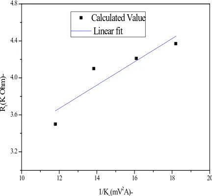
A)-Fig (6)- Plot of Rt versus 1/K0, for different
9
uniformly doped and the channel region is intrinsic. The oxide thickness is 3.5 nm and the silicon film thickness is 4.5nm. R = 5 nm, and 200 ≤ L ≤ 500 nm. For ballistic transport mechanism the length of the device should be smaller than 50nm [7], [8]. Here we considered the device length/circumferences in such a way that it exhibits the typical conventional character. Fig. 2 shows the variation of IDsat versus Gate-Source voltage (VGS) for the device
with L= 400 nm. The dotted point are fitting points for the parabolic dependence of the drain current on gate source voltage that is IDS α(VGS-VT)2. The VGS values are
determined using the extracted source Resistance (Rs) For L=500nm, 400nm, 300nm and 200nm.We have plotted the variation of Transconductance versus the square root of drain source current. Equation (4) reveals the linear relationship of Transconductance and square root of drain source current. From this, we calculated the threshold voltage and K. The mobility-degradation factor is one
order larger than those of planar MOSFETs. For the given configuration, the gate capacitance of the planar MOSFET with the width = 2πR is approximately 0.80 times that of the Gate- All-Around SNWFET. This is due to the large probability of scattering through the interface in GAA structures [8] and for the same magnitude of vertical electric field; the mobility degradation due to the gat
electric field is larger than planar MOSFETs. The
calculated low field mobility μo is comes near about
480 cm2/Vs. which is comparable to typical bulk
nobilities. Therefore, It conform our approach. The calculated series resistance (Rs) is much larger than the usual contact resistance values of planar MOSFETs. We assumed that the devices have large contact pads and bulk source n+ (highly doped) and drain region. The current flow from the contact pad to the nanowire is mainly concentrated on the side surface of the n+ body on which the nanowire is connected
VII CONCLUSION
In this study, the behaviour of carrier mobility in the presented model is discussed by considering the conventional approach. Here, we have successfully examined the values of mobility degradation factor (θ) and Series Resistance (Rs) for long-channel undoped device
with the channel length (L) ranging from 200 to 500 nm. The value of θ is found one order larger than that for planar fully depleted MOSFETs. This large degradation factor reveals the frequent scattering mechanism of electrons in device. Such degradation in mobility is due to excellent gate controllability of the model. The side wall resistance of the presented device is calculated. The data from this calculation satisfy the condition given by equation (4).
REFERENCES
1- Y. Taur and T H Ning, Fundamental of Modern VLSI
Devices (Cambridge: Cambridge University
Press.1998).
2- N. Singh, A. Agarwal, L. K. Bera, T. Y. Liow, R.
Yang, S. C. Rustagi, C. H. Tung, R. Kumar, G. Q. Lo, Balasubramanian, and D. L. Kwong, High performance fully depleted silicon nanowire (Diameter<5nm) gate-all-around CMOS devices, IEEE Electron Device Lett.,27, 5,383(2006).
3- S. D. Suk, S.-Y. Lee, S. M. Kim, E.-J. Yoon, M. S.
Kim, M. Li, C. W. Oh,K. H. Yeo, S. H. Kim, D. S. Shin, K. H. Lee, H. S. Park, J. N. Han, C. J. Park, J. B, Park, D. W. Kim, D.Park, and B. I. Ryu, High performance 5nm radius twinsilicon nanowire MOSFET (TSNWFET): Fabrication on bulk-Si Wafer, Characterestics and reliability. IEDM Tech., Dig., 717(2005).
4- B. Iniguez, D. Jimenze, J. Roig, H. A. Hamid, L.F.
Marsal, and J. Pallares, Explicit continuous model for long channel undoped surrounding gate MOSFETs. IEEE Trans. Electron Devices, 52, 8,1868(2005)
5- ITRS Origination, International Technology
Roadmap for Semiconductor Report-2007Edition,(2007).
6- S M Sze, Semiconductor Devices Physics and
Technology”,(New Delhi:John Wiley and Sons, Inc.).
7- R. Wang, H. Liu, R. Huang, Zhuge, L. Zhang, D. W.
Kim, X. Zhang, D. Park, and Y. Wang, Experimental investigations on carrier transport in silicon nanowire transistors: Ballistic efficiency and apparent mobility. IEEETrans. Electron Devices, 55, 11, 2960(2008). 8- K. H. Cho, K. H. Yeo, Y. Y. Yeoh, S. D. Suk, M.Li, J.
M. Lee, M. S Kim, D. W. Kim, D. Park, B. H. Hong, Y. C Jung, and S. W. Hwang, Experimental evidence of ballistic transport in cylindrical gate-all-aroundtwin silicon nanowire metal-oxide-semiconductor
field-effect-transistors, Appl.Phys.Lett, 92, 5, 052
102(2008).
9- Edwin B. Ramayya, DragicaVasileska, Stephen M.
Goodnick and Irena Knezevic, Electron mobility in Silicon nanowires. IEEE Transcations on Nano Technology, 6,1(2007).
10- Luryi Choi,ByoungHak Hong, Young Chai Jung,
Keun Hwi Cho, Kyoung Hwan Yeo,Dong-Won Kim, Gyo Young Jin, Kyung Seok Oh, Won-Seong Lee, Sang-Hun Song, , Jae Sung Rieh, , Dong MokWhang, and Sung Woo Hwang, Extracting Mobility degradation and total series resistance of cylindrical gate-all-around silicon nanowire transistors. IEEE,Electron DeviceLetters, 30, 6, (2009).
11- M. Wong and X. Shi, Analytical I-V relationship
incorporating field dependent mobility for a symmetrical DGMOSFET with an undoped body. IEEE Trans. Electron Devices, 53(6), 1389 (2006). 12- Duster J S et al 1993, Temperature effects of the
10
Solid State Devices and Materials (Makuhari) (Tokyo: Japan. Soc. Appl. Phys.) pp 835–7.
13- Lalit Singh and B P Tyagi, Electrostatics of Nano
Silicon Transistor, J Nano and Electron Physics, Vol-3, N1 (Part4), pp808-81Vol-3, 2011.