Thermodynamical Phase Noise in Oscillators Based
on
L-C
Resonators
*
Javier Malo, Jose-Ignacio Izpura
Group of Microsystems and Electronic Materials (GMME-CEMDATIC), Universidad Politécnica de Madrid (UPM), Madrid, Spain
Email: [email protected]
Received September 19, 2011; revised October 19, 2011; accepted October 27, 2011
ABSTRACT
Using a new Admittance-based model for electrical noise able to handle Fluctuations and Dissipations of electrical en-ergy, we explain the phase noise of oscillators that use feedback around L-C resonators. We show that Fluctuations produce the Line Broadening of their output spectrum around its mean frequency f0 and that the Pedestal of phase noise far from f0 comes from Dissipations modified by the feedback electronics. The charge noise power 4FkT/R C2/s that disturbs the otherwise periodic fluctuation of charge these oscillators aim to sustain in their L-C-R resonator, is what creates their phase noise proportional to Leeson’s noise figure F and to the charge noise power 4kT/R C2/s of their ca-pacitance C that today’s modelling would consider as the current noise density in A2/Hz of their resistance R. Linked with this (A2/Hz↔C2/s) equivalence, R becomes a random series in time of discrete chances to Dissipate energy in Thermal Equilibrium (TE) giving a similar series of discrete Conversions of electrical energy into heat when the reso-nator is out of TE due to the Signal power it handles. Therefore, phase noise reflects the way oscillators sense thermal exchanges of energy with their environment.
Keywords: Phase Noise; Admittance-Based Noise Model; Fluctuation; Dissipation; Conversion into Heat
1. Introduction
In a previous paper under this title [1] we have shown that when a Positive Feedback (PF) building a voltage in a capacitor is counterbalanced by a Negative Feedback (NF) we called Clamping Feedback (CF), to keep such voltage close to a reference VRef, a Pedestal of electrical
noise was generated. This Pedestal of 50% the amplitude of the native noise but wider bandwidth was due to the confusing action of the 50% noise the CF samples in quadrature with the carrier whose amplitude it aims to sustain in time. This is so because the CF implicit in the Automatic Level Control (ALC) systems or limiters of actual oscillators is phase-locked to the carrier whose amplitude it has to keep in time. This subtle effect was shown in a convenient resonator of 0 , which was a capacitor of capacitance C shunted by a resistance R to account for its losses. Accordingly to [2], losses due to a conductance
0 f
1 G
0
R are a random series of discrete opportunities in time to Dissipate electrical energy in Thermal Equilibrium (TE) and to Convert it into heat out of TE [1]. This resonator was used to build an “oscillator of ” where it was easy to show that the
ampli-tude the CF keeps at each instant is the sum of VRef plus a
small amplitude offset
0
f
Ref
that is the error signal
driving the CF towards its goal: to counterbalance the excess of PF used during the start of the oscillator.When this counterbalance was achieved, this oscillator of
0 sustained a voltage
v V
0
f V0 VRef
Refwhere vε(t) was a constant average value
v t V
v t plus electrical noise superposed to it. The reference VRef(tn)
that the CF needs at instant n to clamp the output ampli-tude was available from the reference VRef(tn–1) at instant
n–1 because VRef
tn VRef
tn1 in this “convenient oscillator”. This availability of VRef(tn), which is notpos-sible when f0≠ 0 because it would require having in ad-vance an electrical reference of the signal the oscillator is going to create, allowed us to show the origin of the aforesaid Pedestal of electrical noise of amplitude 2FkTR
V2/Hz. Whereas the 50% of noise power sampled in phase by the CF was heavily damped as expected, the 50% noise power sampled in quadrature (e.g. “midway” 0˚ for NF and 180º for PF) was enhanced by the CF and gave the aforesaid Pedestal. As we advanced in [1], a similar reasoning for f0 ≠ 0 would require a sinusoidal reference VRef(t) whose generation in advance (e.g. just
before to be used) didn’t help to explain the noise Pedes-tal, whence it can be seen the usefulness of the “resonator *Work supported by the Spanish CICYT under the MAT2010-18933
of 0 ” we handled in [1] for this purpose.
Shunting the R-C parallel circuit of a capacitor with a finite inductance L ≠ 0 one gets an L-C-R parallel reso-nator whose resonance frequency f0≠ 0 allows oscillators repeating phase each
0 f
0 0
T seconds. Actually, this repetition exactly each T0 seconds is impossible, thus meaning that the spectrum of their output signal won’t give a “line” or (f – f0) function. Instead, it will have a non null width due to the charge noise existing in the resonator at temperature T, as we will show. This noise coming from the charge noise of the lossy resonator and from the noise added by the electronics, both collected by Leeson through an effective noise figure F [3], has a
power 4FkT/R C2/s [2]. This charge noise disturbing the otherwise periodic charge fluctuation of the lossless L-C
resonator, not only justifies Leeson’s empirical formula, but also explains the non null width (Line Broadening) of the output spectrum of this type of oscillators [4]. This is possible because the new model [2] not only considers
Dissipations of electrical energy, but also Fluctuations of electrical energy in C that precede the former ones in an electrical Admittance.
1 f
Before handling resonators with f0≠ 0, let’s recall that to sustain the amplitude of their output signal v(t) in time endures to samplev(t) each T0 seconds and the ALC sys-tem or limiter will react from this set of sampled data. Due to the phase noise (jitter in time domain) of the own amplitude thus generated, this sampling won’t be done
exactly each T0 (or each T0/2 seconds by sampling posi-tive and negaposi-tive peaks), although we will consider it as fast and accurate enough to allow the ALC system to handle properly amplitude changes with spectral content up to f0/2 or up to f0 by sampling each T0/2, accordingly to Nyquist sampling theorem. The high speed this sam-pling rate could provide to the ALC system is not used in general because amplitude changes endure energy ones in the resonator. Since the quality factor Q0 of an L-C-R resonator at its resonance frequency is: “π times the life-time of its output voltage v(t) measured in periods T0”, amplitude changes during one period in high-Q resona-tors will be small. Thus, the aforesaid sampling rate will work well for quartz resonators like that of [3], where Q0 factors over 104 are often found. This allows considering that the CF associated to the ALC system or limiter works as expected and since these electromechanical resonators use to be studied by highly selective L-C-R
circuits, our results can be applied to them easily.
2. Dissipation and Feedback-Induced Noise
in an
L-C-R
Resonator
It’s well known that the sinusoidal voltage and current existing at any frequency f in an electrical Susceptance are in-quadrature. To work in parallel mode let’s use the
Admittance function of frequency f 2π whose real part is Conductance G(jω)and whose imaginary part is Susceptance B(jω): Y
j G
j jB
j , where the imaginary unit j means that currents through G(jω) and those through B(jω) are in-quadrature. Considering a sinusoidal voltage existing between the two terminals ofY(jω), currents through B(jω) allow Fluctuations of elec-trical energy in Y(jω) whereas those through G(jω) lead to Dissipations of electrical energy [2]. This is the basis of the new model for electrical noise we will use for
L-C-R resonators that agreeing with [5], is thus a Quan-tum-compliant model leading us to consider Fluctuations
of electrical energy in the Susceptance of these resona-tors together with Dissipations of electrical energy asso-ciated to their Conductance G1R.
Figure 1(a) shows an L-C-R parallel resonator with
losses proportional to the energy stored in C at each in-stant U t
Cv t2
2 p t
v t R2
E because i is
the instantaneous power lost in R. Thus, the energy stored in magnetic form does not produce losses in this resonator. Although these losses represented by R may be due to a resistance RS in series with the inductance LS
of an inductor shunting C, the circuit transform leading to the circuit of Figure 1(a) makes them equivalent to
those of a lossy capacitor shunted by the lossless induc-tance L.
A native LS-C-RS series resonator is thus replaced by its
parallel equivalent circuit of Figure 1(a) to use directly
the new model of [2] for the electrical noise of the Ad-
(a)
(b)
(c)
[image:2.595.343.504.442.688.2]mittance formed by C and R in parallel. This noise comes from a random series of Thermal Actions (TA) that oc-cur in C at an average rate T (TAs per second), given
by [2]:
2 2 T
kT G Rq
1
2 T
T q
R V
(1)
where q is the electronic charge and VT kT q is the
thermal voltage at Temperature T.
Each TA triggers a Device Reaction (DR) aiming to remove the previous Fluctuation of energy in C due to the TA. The use of the parallel circuit of Figure 1(a),
whose noise will come from Fluctuations of electrical energy, has to do with the Cause-Effect or TA-DR pairs producing electrical noise in resistors and capacitors [2], where each TA is a charge noise of one electron. This TA or impulsive displacement current of weight q in C
creates a voltage step v q C
V in C and thus in v(t).
Figure 1(b) shows the time evolution of ∆v(t) after a TA
on C discharged previously, thus showing the DR of this lossy L-C resonator. This DR is a damped oscillation of angular frequency 0 LC 1 2 rad/s and initial am-plitude q C V that can be built from the product of the exponential decay of Figure 1(b) of [1] with amplitude
0 , by a cosine carrier of frequency f0. Since these
random DRs occur in time at the average rate λT of (1), the spectral content of the noise they will give will be like that of Figure 8(a) of [1], but around f0 and with half its bandwidth due to the two times larger time constant (2RC) of Figure 1(b). This is the noise spectrum of the
L-C-R resonator without feedback shown in Figure 1(c),
that will differ from the noise spectrum under the action of the Positive (PF) and Negative (NF) Feedbacks we need to start these oscillators from noise and to keep them oscillating with constant amplitude in time, two tasks that we did in [1] by the counterbalance of an ex-cess of PF by a CF in a convenient oscillator of . V q C
0 f
2RC
0 With an output carrier of non null frequency f0≠ 0 (not the “dc carrier” used to show basic ideas on a CF in [1]) we can speak properly about noise that the CF finds in-phase with the carrier whose amplitude it keeps in time and about noise it finds in-quadrature with it. Added to this, a baseband noise of some kHz bandwidth only occupies a relative narrow band around a carrier with f0
in the tens of MHz for example. This allows using a nar-row-band approach around f0 to speed calculations (e.g. the factor Q0 of the L-C-R of Figure 1(a) is defined at f0, but for Q(f0) = Q0=100, its value and meaning remains
for a sideband frequency 1.001f0). From the above it isn’t difficult to realize that a narrow-band CF working syn-chronously with the carrier at frequency f0≠ 0 will damp well the noise 2FkTR V2/Hz it sees in phase, whereas the noise 2FkTR V2/Hz it sees with phase error of –90˚ will mislead it so as to create the Pedestal of 2FkTR V2/Hz
around f0 shown in [1]. We have to say that this Pedestal
of noise that will lead to a feedback-induced Pedestal of phase noise was not considered in [6] because it is not the random modulation of f0 that we called Technical
phase noise in [1].
It is worth noting that the oscillating voltage of Figure 1(b) decays with 0 , not with E RC
0 f
RC
as one might expect from the R-C circuit used in [1]. The reason is that the energy stored in this L-C resonator not always gives voltage liable to Convert electrical energy into heat as it gave in the R-C circuit of [1]. Due to the (electric magnetic) exchange of energy existing in this resona-tor of 0 , the energy it contains only is in electrical
form half the time on average, as it is shown in Figure 2
for a lossless L-C resonator. This is why the energy pre-sent in an L-C-R resonator with f0 ≠ 0 has two times lar-ger lifetime (U ) than that of the energy present in the resonator with f00 studied in [1] that was
2 RC U
. Hence, the noise spectrum of DRs taking place in the resonator of Figure 1(a) will have half the
bandwidth (e.g. fc/2 around f0, see Figure 3(b)) of the bandwidth found in [1] for the baseband noise of the
L-C-R parallel resonator with L that was
1 2π
C
f f 0
0 C
f f f f
0 f
Hz around 0 (see Figure 3(a)).
Since the noise power Dissipated by R does not de-pend on the L shunting C because Equipartition sets the mean square voltage noise in C [2], the two spectra of
Figure 3 must have the same 4kTR V2/Hz amplitude for
as it will happen in high-Q0 resonators where 0
C . This reasoning becomes less straightforward in
low-Q0 resonators where fC ≈ f0 and they won’t be con-sidered for simplicity. The case with 0 of [1] can help in this case to sketch the aimed noise spectrum.
This reasoning giving directly the spectrum of thermal noise in L-C-R resonators considers that the energy each DR dissipates is no other than the Fluctuation of energy
2 2
U q C
stored by its preceding TA [2] and that the rate λT of TA-DR pairs only depends on R since λT
defines G by (1). It’s worth noting that fC 2 f0
2Q0
(a)
(b)
Figure 3. (a) Noise spectrum of the L-C resonator of Figure 1(a) when its ; (b) Noise spectrum of the L-C reso-nator of Figure 1(a) when its L > 0 is finite.
L
V v V
in Figure 3(b) is the offset ∆f from the carrier frequency
f0 where the Pedestal of Phase Noise [3,7,8] meets the Lorentzian line proposed in [4].
Mimicking what we did in [1] to sustain a dc voltage
0
Ref in C by a CF counterbalancing at
each instant the excess of PF that had built v(t) previ-ously, let’s use again those feedbacks to build a sinusoi-dal voltage v(t) of amplitude V0 in C from its own ther-mal noise and to sustain it in time once it has reached an amplitude close to a reference VRef(t). Knowing that the
ideal L-C resonator for which Figure 2 applies would
sustain a sinusoidal Fluctuation of electrical energy at 2f0 where
v t
1 2
πf LC
0 , Figure 4 shows the PF used to shunt an L-C-R resonator by a resistance –RFB to
over-compensate its losses represented by R. This is done by feeding-back a current
2
FB by the
net-work of transconductance
iFB t v t R 1R
Y FB
V/A, the same type of feedback used in Figure 4 of [1]. For RFB= R, this
PF would compensate exactly the power lost at each in-stant in R, thus the power lost in R at any f. Although this exact compensation will fail at high f because the finite bandwidth BWFB of the feedback of Figure 4, it will
work well at typical oscillation frequencies f0, provided a fast enough electronics is used. Given that the effects of any phase error in the loop due to the finite BWFB and its
associated phase noise were shown in [6], we will con-sider this PF as perfectly in-phase at f0.
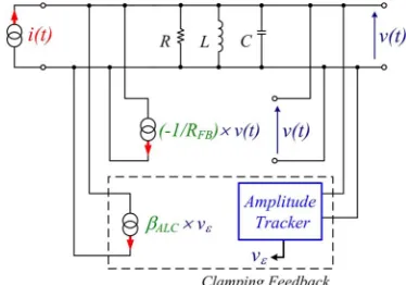
To start the oscillator from thermal noise of C, the PF of Figure 4 has to create a Gain > Losses condition in
the loop (e.g. 1 FB ). Comparing this Figure 4
with Figure 4 of [1] with a similar PF, we can see that
the rectifier D1 of [1] disappears due to the irrelevance of
the sign of the first step ±q/C V of noise that, amplified by the PF during tstart, will build the oscillating v(t)
[image:4.595.95.252.82.251.2]whose amplitude will drive the CF of the ALC system or limiter. Mimicking [1], a NF counterbalances the excess
Figure 4. Feedback scheme of an oscillating loop around the L-C resonator of Figure 1(a) that uses PF to provide loop gain and NF to clamp the output amplitude (see text).
of PF once the aimed amplitude is reached. This is a CF whose implementation was discussed in [1] and that we will simplify by considering that an “amplitude tracker” gives the small error signal 0 Ref required to
drive this CF. Without electrical noise, vε(t) would be the difference between the sinusoidal signal v(t) of amplitude
V0 and a reference signal of the same frequency and phase, but slightly lower amplitude VRef to generate this
error signal. Thus, vε(t) would be a sinusoidal signal synchronous with v(t), with amplitude
v V V
Ref
The
NF of vε(t) through the transconductance βALC would counterbalance at each instant the excess of transcon-ductance ∆βY used during tstart. Using the Clamping
Fac-tor of [1] given by
v V
1 R R
1
VRef v CL
CL1
and considering that ∆βY is driven by v(t), which is times larger than the vε(t) signal driving the CF (see Equation (8) in [1]), the aforesaid counterbalance requires:
1 1 FB
Y ALC ALC
FB R R
CL CL
R R
(2)
Thus, the transconductance βALC that feeds back nega-tively the resonator with the error signal vε(t) will be much higher than the transconductance Y 1RFB
2 T
that allows the reliable start of the oscillator (e.g. by a loop gain start as we used in [1]).
Accepting a 0.1% amplitude error and Tstart = 2 (e.g. RFB = R/2) like those values used in [1] we have: CL =
103. Using these values in (2) we find that the NF coun-terbalancing the excess of PF to clamp the output ampli-tude at 1.001VRef will be shunting the resonator by a
re-sistance RDIF = R/1001. This will be so for any signal
affecting vε(t) as the random series of DRs that form the noise of C. Because DRs appear randomly in time, they endure 50% noise in-phase with vε(t) or with the carrier to which the CF is phase-locked, and 50% noise in- quadrature with vε(t) (recall Figure 7 of [1]). Therefore, the 50% noise power born in-phase with the carrier will be highly damped by the CF (recall Figure 8 of [1])
[image:4.595.328.515.84.215.2]spectrum of density 2kTR V2/Hz around f
0 with
band-width fc) will be enhanced by the broadening of its
spec-trum away from fc/2 [1] as shown in Figure 5. This is
the Pedestal of electrical noise that will exist for separa-tions from the carrier (∆f) higher than fC 2 f0
2Q0
T*T
*
T T
. As we discuss in [1] the width of this Pedestal will depend on the factor Q0 of the resonator and on the loop
gain Tstart and Clamping Factor CL used in the design of
the oscillator. Added to this, the CL of a limiter would have to be taken in an average form, because as the out-put amplitude approaches its limit, the clamping action becomes harder. This means that the bandwidth of the Pedestal shown in Figure 5 is design-dependent and that
is why it has not been specified.
3. Fluctuation-Induced Noise in L-C
Resonators: Thermal FSK or PSK
Modulations
In the model for electrical noise of [2], the voltage noise coming from the DRs taking place in the resonator is the
Effect whose Cause is the series of TAs appearing ran-domly at the average rate T s–1 of (1). Since each DR
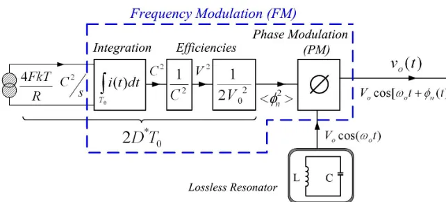
comes from the integration in time of the impulsive cur-rent of each preceding TA, a possible Phase Modulation (PM) of the carrier by DRs will be equivalent to its Fre-quency Modulation (FM) by TAs. This way, the PM ap-proach to Phase Noise of [4] and the FM one of [9] are well understood by the equivalence between FM due to a modulating signal xm(t) and PM due to the time integral
of xm(t). Concerning noise, it’s worth mentioning that
when the L-C-R resonator is in Thermal Equilibrium (TE), its noise spectrum is that of Figure 3(b). No noise
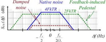
figure F exists in this case because there is neither feed-back electronics nor heating effects that could increase resonator’s temperature as we discuss in [1]. When the PF and CF of the loop balance mutually to sustain the output amplitude V0, the noise increases by F and also split into the damped noise and Pedestal of Fig-ure 5, which shows noise with reference to TE (a native
[image:5.595.87.258.626.694.2]spectrum of density 4kTR V2/Hz increased by the noise of the electronics and by any small heating effect , both included in F) together with two noises that only exist out of TE when the resonator stores the energy
Figure 5. Noise spectra of the L-C resonator of Figure 4 (dotted lines) together with the noise it had in Thermal Equilibrium (solid line) without feedbacks (see text).
UE corresponding to the amplitude V0 of v(t).
Since v(t) is quite a sinusoid let’s have some figures by using v t
V0 sin 2
πf t0
. Therefore, the energy stored in the resonator is: U CV2 2
0
E J and the
aver-age power converted into heat by R (e.g. the mean power leaving the resonator as heat) is: P V2 2R
0 0 . This
leakage of energy per unit time is the price we pay to store UE in this resonator out of TE. Another price we
pay concerns the purity of the voltage v(t) on C because the aimed exchange of energy at 2f0 shown in Figure 2 will be disturbed by the thermal interaction between the resonator and its environment. This exchange of energy represented by R is carried out by a charge noise [2] dis-turbing the otherwise periodic exchange of charge be-tween L and C that would give the sinusoid of V0 volts peak (or CV0 Coulombs peak) we aim to have in C. Con-sidering the distinction made in [1] between power Con-verted into heat and power Dissipated by DRs we can leave aside the power P V2 2R
0 0 assuming that the
small heating of the resonator it will produce
T*T
t
will be included in F. Having considered the effects due to Dissipations of energy in the electrical noise of the loop, we have to consider now the effects due to each Fluctuation of electrical energy preceding each Dissipa-tion because both processes endure a charge noise asso-ciated with Displacement Currents (DiC) in C that dis-turb its otherwise periodic Fluctuation of charge coming from the energy exchange between magnetic and electric susceptances in an L-C resonator. The factor 2 we had to use in [1] to obtain the charge noise power of a series of current pulses mimicking fat TAs, reflected these two charge noises. To say it bluntly, each fast DiC of weight
q in C due to a TA is followed by an opposed and slower DiC of equal weight q and opposed sense linked with its DR. This is why phase noise is a nice scenario to test the validity of the Quantum-compliant model of [2], which was able to explain 1/f excess noise [10] and flicker noise [11] as consequences of thermal noise.
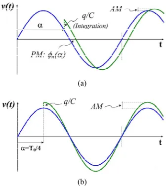
Considering that the damping of a DR during a period of v(t) is small, Figure 6 shows the Phase and Amplitude
changes that a TA produces in the otherwise sinusoidal signal v(t) when it occurs at instant within one period T0. It’s worth realizing that a null damping of this DR triggered by a TA would mean that this resonator has no losses, but having suffered a TA it must be lossy [2]. This contradiction, however, is solved by considering that the damping of a DR in a resonator with only one TA per period (e.g. λT/f0≈ 1) would be vanishingly small: Using (1) at room T, a Q0 ≈ 0.3 C/q would appear. Thus,
Figure 6 is undistinguishable from the true one for
typi-cal L-C-R resonators with Q0 > 50 for example. Since each TA is a charge noise of one electron in C, it always gives the same voltage shift ±q/C V no matter the instant
2 2
2 2
0 0
2 2
2 ( ) sin
2 2 2
TA
Q t q Q t U
C C
q qQ t q qV t
C C C
(a)
[image:6.595.89.257.84.273.2](b)
Figure 6. Effects of a Thermal Action in the capacitance of the L-C oscillator of Figure 4 when the damping of this Fluctuation of energy is small during one period (see text).
(AM) it produces depends on α [7,8], reaching its maxi-mum for α= T0/4 or α= 3T0/4, when the charge in C has
its peak value Qp = CV0 C. From typical circuit values we can say that this non null AM is negligible however, be-cause in an L-C tank with C = 16 pF and V0= 10 V, the peak charge appearing in one of the plates of C is: Qp=
1.6 10–10 C, thus N ≈ 109 electrons. The change of 1 electron in N at α = T0/4 by a TA would be an AM of 0.001 parts per million (–180 dB) that would be lower for AM due to TAs taking place at other instants. Thus, we won’t consider this AM in this introductory paper on phase noise, although it can play a role in high-frequency, low-power oscillators.
The spectrum of the output signal will contain both the Damped and the Feedback-induced Pedestal of noise shown in Figure 5, although the former will be buried by
the Pedestal. Added to them there will be a high line atf0
due to the “carrier” whose amplitude is kept by the CF or better said: a broadened line around f0, because Figure 6 shows an undeniable Phase Modulation (PM) for each TA, except for two among millions that could take place exactly at α = T0/4 or α = 3T0/4. Since each TA displaces one electron in C, it shifts its voltage by
v q C
V depending on its sign and the oscillation continues with new amplitude A and phase (ω0t + ). Thus we have:
0
0sin
A t V sin 0t q C
(3)
Since each TA is an impulsive current unable to change the magnetic energy stored in the resonator (this requires some elapsed time), it only will modify the in-stantaneous energy of C to pass its charge Q(t) to Q(t)
q C. The associated energy change is therefore:
(4)
2 2
U q C
thus equal to the Fluctuation J needed
to displace one electron between plates of C (or to break charge neutrality separating +q and –q charges in C) plus the energy required to move a charge q in a region where charge neutrality already was broken by opposed charges like the dipolar charge of C that is the source of its volt-age V0sin
0t between terminals.The very different scale for ∆U and qV0 in actual cir-cuits appears by considering their ratio qV0/∆U = 2N, for
N being the peak number of electrons in one of the plates of C. For C = 16 pF and V0= 5 V we have: qV0/∆U = 109, thus meaning that the addition of one electron to the negative plate of this circuit needs a 109 times higher energy than the Fluctuation of energy ∆U required to displace one electron between the plates of C with V0 = 0. This huge value raises this question: Where comes from this huge energy when a TA makes an electron to appear as a charge –q on the negative plate of C? A likely source is U C V2 2
0
f f [1], a big energy the free
elec-tron had in the Conduction Band (CB) just before being captured or collected by the negative plate. The ratio
0 0
f T at room T suggests that to
appear as a charge –q at the negative plate of C with V0 = 5 V, the electron borrows a small fraction (1%) of the energy Uf it had as a free carrier in the CB, thus releasing
only 0.99Uf J as heat in the negative plate that collects it.
For a TA of opposed sign in which the electron appeared as a charge –q at the positive plate of C with V0 = 5 V, an energy 1.01Uf J would be released as heat on the positive
plate on its arrival (e.g. the energy Uf it had as a free
car-rier in the CB plus the energy acquired from the electric field in C by an electron passing from its negative plate to its positive one).
2 100
U qV V V
Due to the equal probability for positive and negative TAs, the average energy Converted into heat by each TA is Uf and this account well for Joule effect accordingly to
[1]. Continuing our reasoning from (4), the new ampli-tude A of the oscillation after a TA will come from this energy balance:
2
2 2
0 0 0
1 1 sin
2 2 2
q
CA CV qV t
C (5)
From (4) and (5), the phase shift ∆ produced by a TA
occurring at time t within the period is [12]:
0 0
0 2
2
0 2 0 0
sin arcsin
2 sin
q
V t
C t
q q
A V V t
C C
Using N, the peak number of electrons accumulated in the negative plate of C without TAs, (6) becomes:
00 t t 0 2 sin 1 arcsin
1 2 sin
N t
A N N
(7)
Because TAs have the same probability to increase N
than to decrease it, the average phase shift resulting from (7) for the T TAs per second given by (1) is null, but this
is not so for the mean square phase shift due to the huge amount of TAs taking place within a period T01 f0 of the output signal. Although it’s easy to show that for N
values like those found in actual oscillators (e.g. N > 106) an increment or decrement of one electron gives a similar
∆ shift with opposed sign, we prefer to use the equal number of positive and negative TAs on average to add the square of (7) for a positive TA (e.g. with its signs replaced by + signs) to the square of (7) with its signs replaced by – ones, thus obtaining twice the mean square phase shift of a TA taking place at time t in C. Repre-senting half this sum in the first quarter of period (00tπ 2
t
) we obtain the s-curve shown in Figure 7
by a solid line that represents the square phase shift due to a TA occurring at time
20 N
0 t
within the first quarter of period of the output signal.
For , this averaging of positive and negative TAs is numerically irrelevant and one can take directly the s-curve of Figure 7 from the square of (7) for any
sign of TAs. The dashed line of Figure 7 is the linear
approximation to the s-curve that shows quickly that its mean value in this quarter of period is half its maximum value for 0
, thus 1/2N2. Since this s-curve and
2t 2N2
0t 1 cos
0 fit very well, we can
integrate directly ∆(ω0t) to obtain the same mean value. Therefore, the mean square phase modulation (PM) of each TA is:
2 20 0
1
2 2
q q
C V V
2
2 2 2
1 2
C N
(8)
[image:7.595.100.247.583.696.2]Although (8) is the mean square PM expected for TAs
Figure 7. Square phase-shift due to a Thermal Action as a function of the instant α where it takes place (solid line) and its linear fitting giving its mean square phase shift 1/(2N2).
occurring in the first quarter of the period, the mean square PM expected for TAs occurring in other quarters is the same because the s-curve for π 20tπ
is the mirror image of Figure 7 around π/2, thus an s-curve
increasing from zero to 1/N2. Since (1) is the rate of TAs giving the charge noise power 4kT/R C2/s of the capaci-tance C [2] (usually taken as the noise density 4kT/R
A2/Hz of the resistanceR) the extra noise added by the feedback electronics, collected by the effective Noise Figure F used in [3], leads to multiply (1) by F to collect all the TAs disturbing the resonator per unit time. Thus, the mean square Phase Modulation accumulated during one period T0 by FT TAs per second disturbing the
oth-erwise sinusoidal carrier of amplitude V0, will be:
2 0
0
2π 2
T
E kT
F T F
Q U
(9)
when a period finishes, a new one starts and the phase modulation accumulated in the finished period is lost. Thus the way the phase of v(t) is degraded by TAs as time passes within each period will be:
2 2 2 0 1 n T kTt F t F t
C V RC
(10)
This linear dependence with time comes from the cuasi-linear, cuasi-continuous accumulation of TAs as time passes due to its huge rate FλT. Considering now the Phase Noise model of [4], where the Phase in an ensem-ble of many identical oscillators subjected to white noise diffuses in time, we can consider that this diffusion is a Wiener process whose mean square is given by Equation (3) of [4], which is:
2 2
n t D t
(11)
Thus, this nice model for an ensemble of M identical
L-C oscillators subjected to white noise is formally equal to our single L-C-based oscillator subjected to the white charge noise of [2]. Identifying terms in (10) and (11) we have: * 2 0 0 2 0 0 1 2 1 2 2 kT D F
C V RC
F kT F
D
C V Q
(12) 1
that gives the phase diffusion constant D found in Equa-tion (21) of [4], but multiplied by F/2. This discrepancy concerning F comes from the fact that oscillators used in the theoretical ensemble of [4] have perfect electronics (F ), but the discrepancy concerning the factor 1/2 is more subtle because it is the factor 1/2 that appears for
diffusion constant D handled in [4] by our phase degra-dation constant D* given by (12) that is F/2 times higher
(although its physical meaning is similar) in order to use Equation (3) of [4] for the Lorentzian line that gives the spectral content of the output signal v(t) of our oscillator. Doing it and for D* given in rad/s, we obtain:
2 *
2 0
0 2 * 2 *
V
V D
S V
D D
2
* 1
1
D
(13)
where ∆ω is 2π times the frequency offset f f f0 from the central frequency f0 taken as carrier frequency (see below (3) of [4] for example), although the spectrum of v(t) is not monochromatic, but a Lorentzian line
hav-ing a –3 dB bandwidth *
C
BW D Hz around f0 as (13) shows. Moreover, given the integration in time done by C of each impulsive displacement current or TA to give a voltage step v q C
modulating in phase the “carrier” of static frequency f0, what we have described is the Frequency Modulation (FM) of this carrier at f0 by the impulsive current noise of the TAs. To say it bluntly: the displacement currents generating electrical noise [2] modulate in frequency the aimed carrier of static fre-quency f0 and this shows vividly that v(t) is not a pure sinusoidal carrier giving a spectral line at f0, but a FM carrier whose frequency f(t) wanders randomly with time around f0, tracking the random wandering around zero of the noise current of spectral density 4FkT/R A2/Hz that reflects the thermal noise of C. This noise includes the Nyquist noise traditionally assigned to R, the noise com-ing from the feedback electronics and the extra noise coming from the unavoidable heating of the resonator Converting into heat a power 2
0 0 2
P V R W on
av-erage when it stores the energy UE fluctuating at 2f0. Equation (13) gives the spectral dispersion SV(∆ω) of
the mean-square carrier voltage V2 2
0 of v(t) due to the
effect of TAs (Fluctuations) creating electrical noise in C
[2]. Therefore, SV(∆ω) is a spectral density with the same
units V2/Hz of the noise density S
NV(∆ω) coming from
energy Dissipations shown in Figure 5. Integrating (13)
from to we obtain: 2 0 2
V , thus
indicating that the mean Signal power P V2
2R10
0 f
0 0
converted into heat by R that we have calculated consid-ering v(t) as perfectly sinusoidal, is scattered in a line of non null width around f0. It is worth noting that (13) nothing says about the small, but not null AM of v(t) already discussed concerning Figure 6. A possible
rea-son is that an AM lower than one electron in
is a residual AM lying below –180 dB from V0 itself taken as 0 dB reference, although perhaps the reason is a deeper one because this residual AM dis-appears when the quantization of charge for each TA is neglected, as it would do a noise model unaware about the discrete nature of the electrical charge. In any case,
the power density SV(∆ω) near f0 is so high, that the noise sidebands due to this residual AM will be overridden by it in the same way the feedback-induced Pedestal over-rides the damped noise in Figure 5.
8 109
N
The random noise added by the TA-DR pairs to the sinusoidal v(t) of Figure 6 also can be handled by a small,
randomly-oriented, noise vector AN, added to a big
phasor of amplitude V0 rotating uniformly in time at f0 times per second to represent a “carrier” of static fre-quency f0. This noise vector can be decomposed into a small noise vector AAM along the phasor that represents a
random AM of the carrier, and a small noise vector APM orthogonal to the phasor that represents random PM of the carrier. Due to the random orientation of AN, there is
equal probability for AAM and APM at each instant, thus
meaning that the native noise density 4FkTR V2/Hz of
Figure 5 (e.g. that of the resonator without feedback),
would contain a 50% Amplitude noise and 50% Phase noise added to the carrier. Whereas the ALC system or amplitude limiter would reduce (by design) the 50% AM noise quite effectively, the remaining 50% Phase noise would mislead this system it in such a way that its 2FkTR
V2/Hz density would be extended up to frequencies well above f0/(2Q0), being this the Pedestal of electrical noise shown in Figure 5. We could say that the Pedestal of
noise of Figure 5 only is Phase noise of the resonator
amplified by the ALC system or limiter designed to re-duce amplitude noise because electrical noise contains both Amplitude as well as Phase noise when the ALC system is phased locked to a frequency 0 .
The Pedestal of 2FkTR V2/Hz shown in
Figure 5 leads
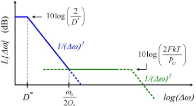
to the Pedestal of Phase noise shown in Figure 8, where
it appears together with SV(∆ω) given by (13), both nor-malized by the mean-square carrier voltage V2 2
0 in
order to have the familiar single-sideband spectral den-sity of Phase Noise L{∆ω} found in Equation (12) of [7] for example. Using (12) in (13) to find the frequency offset ∆fF-D where SV(∆ω) drops down to 2FkTR V2/Hz or
where the phase noise due to Fluctuations of energy in C
and the phase noise due to Dissipations of energy in R
modified by the feedback are equal, we obtain:
0 0
F D
f f 2Q
as shown in Figure 8. This result
harmonizes the Line Broadening proposed in [4] with Lesson’s formula concerning the transition from a region where phase noise varies as 1/(∆ω)2 to a Pedestal of Phase Noise far from f0 [3]. Added to the above, Leeson also gave a region where Phase Noise passed to vary as 1/(∆ω)3 as we approach more f
0 [3], a region that does not appear in Figure 8. This is so because we haven’t
Figure 8. Lorentzian line of phase noise (“carrier” line) due to Thermal Actions in C, together with the phase noise ped-estal generated by the clamping feedback (see text).
Recalling what we wrote about (13): that its Lorentzian Line reflects a FM of the carrier of frequency f0 by a noise of flat spectrum that is F times the Nyquist noise current usually assigned to R, we can explain easily the region of Phase Noise varying as 1/(∆ω)3 that appears in oscillators, especially in those using resonators of high
Q0 (thus ) and with electronics bearing 1/f-like noise below some frequency fCN, no matter if it is excess
noise (resistance noise in Solid-State devices [10]) or flicker noise (flux noise in vacuum ones [11]). As we wrote under (13), the output power of the oscillator ap-pears within a –3 dB bandwidth
* 0
D
* π
BW D
*
D
C Hz
around f0. From (12), the constant D* for resonators with
high Q0 values is correspondingly low. This is why the
phase noise found in these oscillators uses to be the re-gion of (13) where it is proportional to 1/(∆ω)2, a “skirt” of Phase Noise that drops down to the Pedestal as ∆ω
increases for . Let’s consider the Phase Noise of these oscillators that use high Q0 resonators when the
flat spectrum of noise that modulates in Frequency the carrier is filtered previously by a low-pass filter with cut-off frequency fcol col
2 f0
2Q0
.Figure 9(a) shows the spectrum of this filtered noise
modulating the carrier of static frequency f0 and Figure
9(b) shows the Phase Noise spectrum it produces. The
Phase Noise roll-off changes from 1/(∆ω)2 for
col
Thus, a sum of low-pass filtered noise spectra like those of Figure 10(a) that synthesize a region of 1/f
noise, will give the Phase Noise spectrum of Figure 10(b)
with a region of Phase Noise proportional to 1/(∆f)3, as the empirical one reported by Leeson [3].
Considering that the 1/f noise of Solid-State devices is synthesized in the way shown in Figure 10(a) [10] and
that the flicker noise of vacuum tubes with 1 f with
1
also comes from a similar synthesis process [11],
(a)
(b)
Figure 9. (a) Low-pass filtered white noise modulating in frequency (FM) a carrier of static frequency f0; (b) Energy spectrum of the FM carrier thus obtained represented as Phase Noise around f0 (see text).
to 1
4 for col, an effect due to the integra-tion of the modulating signal that precedes the Phase Modulation in a Frequency Modulator. This integration in t leads to a term inversely proportional to the modu-lating frequency fm, whose effect in the phase noisespec-trum appears at m
(a)
. Hence, the flat spectrum of the modulating signal gives phase noise proportional to 1/(∆ω)2 whereas the region whose power density drops as 1/(ωm)2 gives phase noise proportional to 1/(∆ω)4. From this fact, it is easy to understand that a sum of the above low-pass filtered signals will give a sum of Phase Noise spectra like that of Figure 9(b), because the FM
modulator we are handling is linearand time-invariant. With our new noise model [2] we don’t need to abandon time-invariance as it is done in [7,8].
(b)
[image:9.595.365.483.204.422.2] [image:9.595.350.496.486.685.2]Figure 11. Embedded FM modulator existing in oscillators based on L-C resonators due to the Thermal Actions that the new model for electrical noise identifies with the charge noise power 4FkT/R C2/s existing in C at temperature T due to its losses represented by R and to its noise figure F.
we have shown the origin of Phase Noise varying as 1/(∆f)3. As a way to show the mechanism giving the Line Broadening of the output spectrum of oscillators based in
L-C resonators, Figure 11 summarizes the Charge
Con-trolled Oscillator (CCO) we have when we use an L-C
resonator and feedback electronics aiming to sustain a periodic Charge Fluctuation at f0 in this resonator at temperature T. This CCO models the Line Broadening around f0 of these oscillators that will be a Lorentzian line for white current noise and that will have another shape if the current noise modulating the carrier is “col-oured” noise. This Phase Noise around f0 is the random Phase Modulation of the carrier by DRs (or its random FM by TAs) that one obtains neglecting the decay of each DR within one period of v(t), thus being valid for resonators with negligible Dissipation (e.g. Q0 > 50). Since each DR really decays as it dissipates the electrical energy stored in C by its preceding Fluctuation or TA, these random decays also generate electrical noise of bandwidth fC/2 around f0 whose power in-quadrature with the output signal mislead the CF designed to reduce amplitude noise, thus producing the Pedestal of phase noise 2FkT/P0 that accompanies their carrier Line Broadening and that the FM modulator of Figure 11
does not take into account.
4. Conclusions
Using a new model for electrical noise based on Fluctua-tion-Dissipation of electrical energy in an Admittance, the Phase Noise of resonator-based oscillators is ex-plained as a simple consequence of thermal noise. The discrete Fluctuations of energy involving single electrons produce the observed Line Broadening whereas the noise associated to subsequent Dissipations modified by the feedback electronics, lead to the Phase Noise Pedestal far from the “carrier”. Therefore, a monochromatic carrier of static frequency f0 never is obtained and the oscillator’s
output corresponds to a Frequency Modulated carrier of central frequency f0 whose instantaneous frequency f(t) wanders randomly with time around f0, tracking the ran-dom wandering of the noise current of density 4FkT/R
A2/Hz that collects the noise of the resonator, its elec-tronics and the extra noise due to any heating effect due to the Signal power converted into heat in the resonator. In summary: Phase Noise shows the way the oscillator senses the charge noise power 4FkT/R C2/s that exists in its L-C resonator while it stores the energy corresponding to the output signal it sustains in time because these os-cillators always are CCOs driven by the charge noise of their capacitance.
REFERENCES
[1] J. I. Izpura and J. Malo, “Thermodynamical Phase Noise in Oscillators Based on L-C Resonators (Foundations),”
Circuits and Systems, 2011, Article in Press.
[2] J. I. Izpura and J. Malo, “A Fluctuation-Dissipation Model for Electrical Noise,” Circuits and Systems, Vol. 2, No. 3, 2011, pp. 112-120. doi:10.4236/cs.2011.23017 [3] D. B. Leeson, “A Simple Model of Feedback Oscillator
Noise Spectrum,” Proceedings of IEEE, Vol. 54, 1966, pp. 329-330. doi:10.1109/PROC.1966.4682
[4] D. Ham and A. Hajimiri, “Virtual Damping and Einstein Relation in Oscillators,” IEEE Journal of Solid-State Circuits, Vol. 38, No. 3, 2003, pp. 407-418.
doi:10.1109/JSSC.2002.808283
[5] H. B. Callen and T. A. Welton, “Irreversibility and Gen-eralized Noise,” Physical Review, Vol. 83, No. 1, 1951, pp. 34-40. doi:10.1103/PhysRev.83.34
[6] J. Malo and J. I. Izpura, “Feedback-Induced Phase Noise in Microcantilever-Based Oscillators,” Sensors and Ac-tuatorsA, Vol. 155, No. 1, 2009, pp. 188-194.
doi:10.1016/j.sna.2009.08.001
[8] A. Hajimiri and T. H. Lee, “A General Theory of Phase Noise in Electrical Oscillators,” IEEE Journal of Solid- State Circuits, Vol. 33, No. 2, 1998, pp. 179-194. doi:10.1109/4.658619
[9] E. Hegazi, J. Rael and A. Abidi, “The Design Guide to High Purity Oscillators,” Kluwer Academic, New York, 2005.
[10] J. I. Izpura, “1/f Electrical Noise in Planar Resistors: The Joint Effect of a Backgating Noise and an Instrumental Disturbance,” IEEE Transactions on Instrumentation and Measurement, Vol. 57, No. 3, 2008, pp. 509-517.
doi:10.1109/TIM.2007.911642
[11] J. I. Izpura, “On the Electrical Origin of Flicker Noise in Vacuum Devices,” IEEE Transactions on Instrumenta-tion and Measurement, Vol. 58, No. 10, 2009, pp. 3592- 3601. doi:10.1109/TIM.2009.2018692
![Figure 1(a)the new model of [2] for the electrical noise of the Ad-](https://thumb-us.123doks.com/thumbv2/123dok_us/9247665.412684/2.595.343.504.442.688/figure-new-model-electrical-noise-ad.webp)