University of Warwick institutional repository:http://go.warwick.ac.uk/wrap
A Thesis Submitted for the Degree of PhD at the University of Warwick
http://go.warwick.ac.uk/wrap/71005
This thesis is made available online and is protected by original copyright. Please scroll down to view the document itself.
Nanostructured Copper Electrodes for
Organic Photovoltaics
By
Oliver Samuel Hutter
A thesis submitted for the degree of
Doctor of Philosophy
Supervised by
Dr. Ross A. Hatton
Department of Chemistry,
University of Warwick, UK
2
Abstract
This thesis describes a body of original research focused on the development of a viable
alternative to the indium-tin oxide (ITO) glass window electrode used in organic
photovoltaic (OPV) devices, based on the use of ultra-thin Cu films.
The first results chapter describes a low cost, robust Cu | Al bilayer window
electrode that simultaneously functions as the low work function electron-extracting
electrode and as a sink for oxygen/water molecules in OPVs. When the electrode is
exposed to air, an ultra-thin oxide layer forms at its surface without any increase in
surface roughness, and the sheet resistance of the electrode actually decreases. However,
this electrode has the disadvantage of a lower far-field transparency than ITO glass. The
second results chapter describes how the transparency of ultra-thin Cu films can be
increased to a level comparable to that of ITO glass across most of the spectrum over
which OPVs harvest light using an overlayer of tungsten sub-oxide (WO3-x) which is
spontaneously doped with Cu, increasing both its refractive index and electrical
conductivity. Unfortunately these electrodes are not air stable. The third results chapter
describes how the developments described in the previous two chapters might be
integrated to realise an electrode that is both air-stable and highly transparent. The final
results chapter describes a very different approach to coupling light into an OPV based on
a Cu electrode with a dense array of sub-optical wavelength apertures. These electrodes
absorb light strongly, concentrating it as surface plasmon excitations. It is shown that this
trapped light can be absorbed by the light harvesting organic semiconductor in organic
photovoltaics so that electrodes with very low far-field transparency can perform as well
3
Table of Contents
Abstract 2
Acknowledgements 7
List of Publications 8
Declaration 9
Abbreviations and Acronyms 10
List of chemicals and compounds 12
Chapter 1- Introduction 14
1.1 Context 14
1.2 Existing Photovoltaic Technologies 15
1.3 Organic Semiconductors 16
1.5 Principles of Organic Photovoltaic (OPV) Operation 22
1.5.2. Device Parameters and Characteristics 27
1.6 OPV stability 29
1.7 OPV materials 30
1.7.1- Material 1- Supporting Substrate 32
1.7.2- Material 2- Electron Donor Material 33
1.7.3- Material 3- Electron Acceptor Material 37
4
1.9 ITO Problems 41
1.10 ITO Alternatives 42
1.10.1 Alternative Oxides 43
1.10.2 Carbon Based Nanomaterials 43
1.10.3 Conducting Polymers 44
1.10.4 Metal Nanowires 44
1.10.5 Metal Grids 44
1.10.6 Ultra-thin metal films 45
1.12 Metal Oxides in OPVs 46
1.13 Plasmonics 49
1.14 Project Overview 52
Chapter 2 – Experimental Techniques 53
Summary 53
2.1 Substrate Preparation 53
2.1.1 Substrate cutting and cleaning 53
2.1.2 UV/O3 treatment 55
2.2 Metal and Monolayer Deposition 56
2.2.1 Metal Evaporation 56
2.2.2 Self-assembled Monolayer (SAM) Deposition 56
2.3 Substrate/ Electrode Characterisation 58
2.3.1 Sheet Resistance Measurements 58
2.3.2 Optical Measurements 59
2.3.3 Kelvin Probe Technique 60
5
2.3.5. Scanning Electron Microscopy 64
2.3.6. Ellipsometry Measurements 65
2.3.7. Static-Secondary Ion Mass Spectrometry: 66
2.3.8 X-ray Photoelectron Spectroscopy 66
2.3.9 Ultra-violet Photoelectron Spectroscopy 68
2.4 Device Fabrication 70
2.4.1 Organic Semiconductor and Metal Oxide Deposition 70
2.4.2 Device Shadow Masks and Device Layout 73
2.4.3. Spin Coating and Device Annealing 74
2.5 Device Testing 76
2.5.1 Current Density- Voltage Testing 76
2.5.2 External Quantum Efficiency Measurements 77
2.5.3 Data Analysis 79
2.5.4 Optical Simulations 79
2.5.5 Degradation Measurements 79
Chapter 3 – Ultra-thin Cu/Al Electrodes 81
3.1 Abstract 81
3.2 Background 81
3.3 Experimental 84
3.4 Results and Discussion 85
3.5 Conclusions 101
Chapter 4 – Hybrid Copper: Doped Tungsten Sub-oxide Window
6
4.1 Abstract 102
4.2 Background 102
4.3 Experimental 104
4.4 Results and Discussion 106
4.5 Conclusions 133
Chapter 5 – Achieving Stability and Transparency in Cu Window
Electrodes 134
5.1 Abstract 134
5.2 Background 134
5.3 Experimental 135
5.4 Results and Discussion 135
5.5 Conclusions 147
Chapter 6 – Plasmon-active Cu Electrodes 148
6.1 Abstract 148
6.2 Background 148
6.3 Experimental 153
6.4 Results and Discussion 154
6.5 Conclusions 185
7. Conclusions and Future Work 186
7
Acknowledgements
I would like to thank Warwick University for the Chancellor’s Scholarship which funded
me to carry out this research.
I would like to thank Dr. Josephine Bunch (University of Birmingham), for
assistance with collecting the s-SIMS data, Dr. Marc Walker (University of Warwick,
Department of Physics) for assistance with the XPS and UPS data collection and
Professor Tim S. Jones for use of his group atomic force microscope and other laboratory
equipment. I would like to thank the Jones group for all of their technical support
throughout the project, particularly Dr. Paul Sullivan, who helped train me on many
pieces of equipment.
I would like to thank everyone in the Hatton research group including Martin
Tyler, Kenny Marshall and Helena Stec. I’d also like to thank Luke Daniels for his help
and support with my many queries along the way. I’d like to thank my parents, without
their love and care I could achieve very little in this world.
Lastly I would like to thank Ross, whose door was always open to me; his
support and guidance throughout my PhD have been brilliant and I feel very privileged to
8
List of Publications
“An Indium-Free Low Work Function Window Electrode for Organic
Photovoltaics Which Improves with In-Situ Oxidation” O.S. Hutter, H.M. Stec, R.
A. Hatton, Adv. Mater.2013, 25, 284.
“A Hybrid Copper:Tungsten Suboxide Window Electrode for Organic
Photovoltaics” O.S. Hutter, R.A. Hatton, Adv. Mater.2015, 27, 326.
Patents
9
Declaration
The work presented in this thesis was conducted at the Department of Chemistry,
University of Warwick in Coventry with the exception of the X-ray photoelectron
spectroscopy (XPS), ultra-violet photoelectron spectroscopy (UPS), and secondary ion
mass spectrometry (SIMS) measurements. The XPS and UPS measurements were carried
out in the Department of Physics, University of Warwick with the assistance of Dr. Marc
Walker, and the SIMS measurements were carried out in the Department of Chemistry,
University of Birmingham with the assistance of Dr. Josephine Bunch. All data collection
was performed by me with the exception of the reflectivity of thick Ag and Al films
(Figure 6.25), which was recorded by Martin Tyler. I confirm that none of the work
included has previously been submitted for a higher degree. Parts of the work have been
patented, published in scientific journals and were presented at conferences, symposiums
10
Abbreviations and Acronyms
AFM: Atomic force microscopy
AM1.5: Air Mass 1.5
AOs: Atomic orbitals
BHJ: Bulk heterojunction
CB: Conduction band
DMD: Dielectric metal dielectric
DSSC: Dye sensitized solar cells
Ef : Fermi level
Eg: Band gap
EQE: External quantum efficiency
FF: Fill factor
HOMO: Highest occupied molecular orbital
HOPG: Highly orientated pyrolytic graphite
HPLC: High performance liquid chromatography
IPCE: Incident photon to converted electron
JMPP: Current density at the maximum power point
Jsc: short circuit current density
LUMO: Lowest unoccupied molecular orbital
11 kWh: Kilowatt hour
OFETs: Organic field effect transistors
OLEDs: Organic light emitting diodes
OPV: Organic photovoltaic
PCE: Power conversion efficiency
PV: Photovoltaic
QCM: Quartz crystal microbalance
RMS: Root mean squared
rpm: Revolutions per minute
RS: Series resistance
RSH: Sheet resistance
RSHUNT: Shunt resistance
SAM: Self-assembled monolayer
SPP: Surface plasmon polariton
SPR: Surface plasmon resonance
UV: Ultra-violet
VB: Valence band
VL: Vacuum level
VMPP: Voltage at the maximum power point
12 XPS: X-ray photoelectron spectroscopy
%T: %Transmission or %transparency
Φ: Work function
Ω sq-1
: Ohms per square
List of chemicals and compounds
APTMS: (3-aminopropyl)trimethoxysilane
BCP: 2,9-dimethyl-4,7-diphenyl- 1,10-phenanthroline or Bathocuproine
CdTe: Cadmium telluride
CIGS: Copper indium gallium selenide
CNT: Carbon nanotube
ClAlPc: Chloroaluminium phthalocyanine
C60: Buckminster fullerene
IPA: Isopropanol
ITO: Indium-tin oxide
MPTMS: (3-mercaptopropyl)trimethoxysilane
PCDTBT:Poly[N-9'-heptadecanyl-2,7-carbazole-alt-5,5-(4',7'-di-2-thienyl-2',1',3'-benzothiadiazole)]
13 PC70BM: 30H-cyclopropa[8,25][5,6]fullerene-C71-D5h(6)-30-butanoic acid, 30-phenyl-,
methyl ester
PEDOT:PSS: poly(3,4-ethylenedioxythiophene):poly(styrenesulfonate)
PEN: Polyethylene naphthalate
PET: Polyethylene terephthalate
PTB7: poly- [[4,8-bis[(2-ethylhexyl)oxy]benzo[1,2-b:4,5-b0]dithiophene-2,6-diyl]-
[3-fluoro-2-[(2-ethylhexyl)carbonyl]thieno[3,4-b]thiophenediyl]
P3HT: Poly(3-hexylthiophene-2,5-diyl)
Spiro-OMeTAD: 2,2(,7,7(-tetrakis-(N,N-di-pmethoxyphenylamine)9,9’-spirobifluorene
14
Chapter 1- Introduction
1.1 Context
Energy demand is currently soaring due to the increasing world population, which is
expected to saturate at ~9 billion people in 2050,1 and the increasing affluence per capita
of many nations. The latter is in large part due to the industrialisation of the very
populous nations of India and China.
With global warming due to greenhouse gas emissions, particularly CO2, giving
rise to climate change,2 low carbon and renewable sources of energy are needed now
more than ever. Nations are also striving to secure energy independence, which is driving
the development and uptake of renewable energy technologies.2
The development and implementation of renewable energy technologies has
grown hugely in the past decade; for example, the generation capacity of photovoltaic
(PV) panels increased ten-fold between 2000 and 2011.3 Substantial proportions of many
nations’ electricity demands are already generated by renewable energy technologies,
with renewable energy supplying 18% of the United Kingdom’s electricity in the last
quarter of 2013.4 In 2013 the United Kingdom produced 28% more electricity from
renewable sources than in the previous year, despite overall electricity generation falling
2% in the same period due to more efficient use of energy.4 Each different renewable
energy technology has its own output variability; for example PVs do not produce
electricity at night and the generating capacity varies continuously throughout the day.
Thus a mix of renewable technologies is often beneficial for power generation on a large
scale. Two billion people currently live without a connection to grid electricity and so
15 of use is therefore an important challenge. PVs are a very promising option for achieving
this.
PVs are the second most studied renewable energy technology after wind
turbines.5 This is due to the many advantages of PVs including low operating costs,
portability, and use as a source of power at the point of use without the need for a grid
connection. With the sun delivering more energy to earth in one hour than humanity uses
in one year,6 and the cost of electricity generated using PVs already near to grid parity in
some sunnier parts of the world,7 PV technologies are now beginning to play a pivotal
role in the energy sector.
1.2 Existing Photovoltaic Technologies
The archetypal PV device is based on inorganic materials and has an active layer made of
either mono or poly-crystalline silicon. This type of PV offers a power conversion
efficiency (PCE) of up to ~25% and excellent stability which results in operational
lifetimes of up to 30 years.8 Over the past 40 years the cost of producing silicon PVs has
fallen drastically and PCE has steadily increased, reducing the cost per watt of electricity
they generate to a level comparable with other more established renewable technologies.9
However, inorganic PV modules are still relatively expensive to produce due to the large
amount of energy required in the material purification and processing stages.
Polycrystalline silicon PVs are lower cost than monocrystalline PV, but are still more
expensive than third generation PV technologies based on thin films.
In addition to first and second generation PVs, there are many new PV
technologies being researched, including organic photovoltaics (OPVs), perovskite
PVs,6,10 dye sensitised solar cells (DSSC),11 copper indium gallium selenide (CIGS)
16 semiconductors. These thin film PVs are advantageous as they use much less active
material (layer thickness ˂ 1 µm) than crystalline Si PVs (layer thickness > 100 µm),15
which reduces the cost of materials, processing speed and energy required in their
fabrication.
All thin film PVs have different stabilities, PCE and fabrication costs and so are
matched to different potential applications. OPVs have the potential to be one of the
lowest cost of all emerging thin film PV technologies due to the very low semiconductor
film thickness and the possibility of processing organic semiconductors at low
temperatures from solution.16 Thus, OPVs have strong potential to deliver a
transformative reduction in the cost of generating electricity directly from sunlight.17-19
However, OPVs like all other thin film PV technologies require a transparent electrode,
and the existing industry standards are too expensive and poorly matched to the needs of
OPV.
1.3 Organic Semiconductors
Organic semiconductors are highly conjugated carbon based molecules that have
conduction properties between those of metals and insulators. Organic semiconductors
typically have a band gap of 2-3 eV and can be small molecules (e.g. C60, Figure 1.17) or
polymeric materials (e.g. poly-
[[4,8-bis[(2-ethylhexyl)oxy]benzo[1,2-b:4,5-b0]dithiophene-2,6-diyl]-[3-fluoro-2-[(2-ethylhexyl)carbonyl]thieno[3,4-b]thiophenediyl]
(PTB7), Figure 1.13). This class of semiconductor are molecular solids and so their bulk
properties are dominated by those of the individual molecules.
When atoms are brought together to form molecules, their atomic orbitals (AOs)
spatially overlap and some of the valence AOs merge to form molecular orbitals (MOs),
17 bonding (lower energy), or anti-bonding (higher energy) MOs. In an organic
semiconductor, often the s and two of the p AOs of carbon form sp2 hybridised orbitals,
which make up the σ bonded framework of the molecule. The remaining p AOs which are
out of the plane of the σ bonded framework then form delocalised π molecular orbitals at
higher energies than their σ counterparts, which give rise to the optical and electronic
properties of organic semiconductors. The highest occupied molecular orbital (HOMO) in
a molecule consists of π bonding MOs and the lowest unoccupied molecular orbital
(LUMO) comprises π anti-bonding MOs as illustrated in Figure 1.1. The HOMO and
LUMO in an organic semiconductor are equivalent to the valence band (VB) and
conduction band (CB) edges respectively in an inorganic semiconductor.
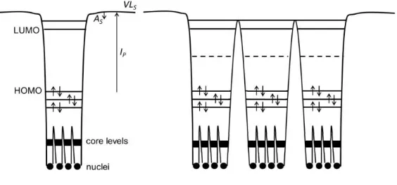
Figure 1.1: The energy levels of an isolated organic molecule (left) and a molecular solid
(right), with individual atoms / molecules depicted as potential wells.20 Ip, VLS and AS
correspond to the ionisation potential, the vacuum level at the surface and the solid state
electron affinity respectively.
The difference between the VB and the CB edges is known as the band gap (Eg).
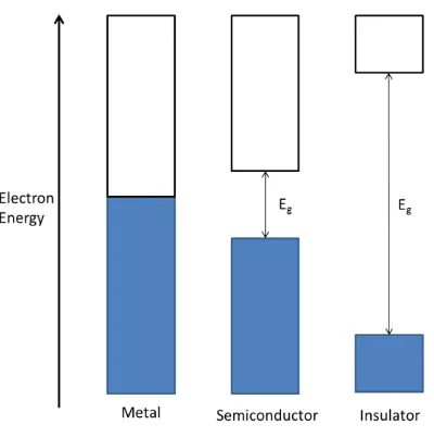
Insulators have large band gaps (>3 eV), conductors have a band gap equal to zero (i.e. a
[image:18.595.191.473.371.503.2]18 as illustrated in Figure 1.2. Thermal excitation of electrons across the band gap in
intrinsic semiconductors at room temperature is minimal and so free charge carriers in
semiconductors required for appreciable conduction are produced by the injection of
electrons (or holes) into the CB or VB using an electric field or by photo-excitation of
electrons from the VB to the CB.
Figure 1.2: Schematic energy level diagrams of a metal, semiconductor and an insulator
are shown from left to right. Occupied bands are depicted in blue, with unoccupied bands
in white.
The HOMO-LUMO gap in an organic semiconductor is the primary determinant
of its colour; for example, the Eg of
poly[N-9'-heptadecanyl-2,7-carbazole-alt-5,5-(4',7'-di-2-thienyl-2',1',3'-benzothiadiazole)] (PCDTBT) is ~1.9 eV, which corresponds to an
absorption onset at 650 nm.21 This is in the red part of the spectrum, so this
semiconductor is purple in colour. The Eg combined with the accessibility of the frontier
orbitals (HOMO and LUMO) determines the electrical properties of the material in a
[image:19.595.233.433.220.421.2]19 Organic semiconductors typically have low charge carrier mobilities because
charge carriers must hop between the potential wells associated with each molecule, and
high electric field strengths are therefore required to inject/extract charge carriers.
Consequently, very thin active layer thicknesses of typically ˂200 nm are used in OPVs.
The primary advantage of organic semiconductors over conventional inorganic
semiconductors for PV applications is that they can be processed at low temperature from
solution, which should enable rapid production of low cost PV modules.
1.4
Organic Photovoltaics
The heterojunction OPV was first reported by Tang in 1986, with a PCE of ~1% and was
based on a bilayer of electron donor and electron acceptor type molecules.22 However, it
was not until the turn of the century that this PCE was increased from ~1% to above 11%
in 2013;23 a level considered to be sufficient for commercialisation.24-26 This rapid
progress stemmed from the invention of the bulk-heterojunction (BHJ) device structure; a
complex interpenetrating blend of electron donor and electron acceptor type molecules.
This progress is illustrated in Figure 1.3, which shows the peak efficiency for laboratory
20
Figure 1.3: Certified PCE values for lab scale single layer solution processed OPVs
which were published in the journal Progress in Photovoltaics, taken from Scharber et
al.23
OPVs have the potential to be a cost effective alternative to inorganic PVs in
some applications27 including for off-grid power generation in developing countries.7,28
Their light weight and low profile as compared to inorganic PVs also makes them
attractive for transport applications. Other potential advantages of OPVs over
conventional Si PVs include (i) lower production costs due to the thin film architecture;
(ii) the possibility of rapid roll-to-roll production; (iii) low energy input during
fabrication translating to very low CO2 emissions per KWh of energy generated; (iv) the
possibility of semi-transparent modules enabling integration with windows.28 However,
issues with stability are prevalent, the PCEs are lower, and this technology is still
essentially pre-commercialised.28 With fast roll-to-roll production methods enabling OPV
modules to be produced at low cost and at high speed, energy payback times of 180 days
[image:21.595.187.469.71.286.2]21 the PV system to generate the equivalent amount of energy consumed in the construction
and decommissioning phases”.28 Energy payback times as short as one day have been
forecast for OPVs.17
The main challenges in OPV research are to increase the PCE and the stability,
whilst maintaining the cost advantage over conventional PV technologies. Novel organic
polymeric materials for active layers of OPVs are a key step in driving up the PCE
values,30 as narrow band gap electron donor materials are required to harvest more of the
solar irradiance (Figure 1.4).
Figure 1.4: The air mass 1.5 (AM1.5) solar irradiance (black) and photon flux (red).31
Since most organic semiconductors are susceptible to photo-oxidation, device
lifetimes can be improved by blocking the ingress of O2 into the photoactive layer, and so
a great deal of research effort is currently directed at the development of low cost
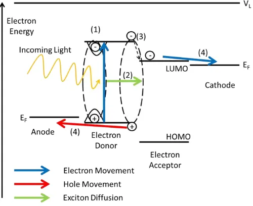
22 1.5 Principles of Organic Photovoltaic (OPV) Operation
In an OPV, light enters the device through a transparent electrode, and is absorbed by the
light harvesting organic semiconductor layer. Upon light absorption a Frenkel exciton is
formed, which is a coulombically bound electron and hole pair on the same molecule
(Figure 1.5, step 1). Frenkel excitons typically have binding energies of 0.2-1 eV in
organic semiconductors and diffuse between molecules (Figure 1.5, step 2), visiting 102
-103 individual molecules before relaxation to the ground state. Frenkel excitons can be
dissociated into free electrons and holes at the junction between two different types of
organic semiconductor having offset frontier orbital energies such that one serves as an
electron donor to the other. Examples of organic semiconductors with donor and acceptor
type character are given in Section 1.8 of this thesis. This junction is called a
heterojunction due to the abrupt discontinuity in HOMO and LUMO levels. The electron
accepting material then transports the free electron to the cathode and the electron
donating material transports the free hole to the anode (Figure 1.5, step 4). The electron
donor material is therefore the organic semiconductor that will donate electrons into the
LUMO of the electron acceptor from the electron donor’s LUMO at the heterojunction
23
Figure 1.5: Schematic energy level diagram for an OPV device. The flow of electrons
(blue) and holes (red) through the HOMOs and LUMOs respectively is shown.
Splitting of excitons at the organic heterojunction can occur with near 100%
efficiency.33 There is however only a limited distance an exciton can diffuse before it
relaxes to the ground state, since the lifetime of a singlet exciton is of the order of 1 ns.33
Triplet excitons are longer lived although more strongly bound and so more energy is
required to dissociate them. The small exciton diffusion length in organic semiconductors
constrains the organic semiconductor layer thickness in a simple bilayer device to tens of
nms at most.
A BHJ is a complex interpenetrating network of donor and acceptor phases
which are separated on a scale close to the exciton diffusion length in both materials
(Figure 1.6). This architecture ensures all excitons formed in either phase are within a
[image:24.595.205.455.78.282.2]24 layers. However, the resistance to charge carrier extraction is increased due to a less
direct path to the electrodes.
Figure 1.6: Schematic illustration of a bilayer (left) and BHJ (right) device architecture,
with the electron donating material (blue), electron accepting material (red) and the
electrodes depicted at the top and bottom.
The light harvesting part of the device is also known as the photo-active layer
and is usually 50-300 nm thick.7 The domain size and morphology of the active layer is a
critically important factor in determining BHJ device PCE.30
OPV device structures can be categorised as either conventional or inverted. In
the conventional configuration the transparent substrate electrode is the hole extracting
electrode, and in the inverted structure it is the electron extracting electrode. Inverted
OPV systems yield comparable or higher efficiencies than their conventional counterparts
and improved stability.35
Figure 1.7: A conventional architecture bilayer OPV device with charge extraction
25 (blue) and the opaque low work function top electrode. The hole extracting interlayer is
in contact with the electron donor (green) and the bottom high work function window
electrode.
OPVs also include charge extraction or buffer layers (Figure 1.7) which can
perform a number of functions including (i) tuning the interfacial energetics to optimise
the efficiency of free charge carrier extraction; (ii) enabling selective extraction of one
charge carrier type; (iii) blocking diffusion of metal ions from the electrodes into the
organic semiconductors;36 (iv) acting as an optical spacer for enhanced light absorption;
(v) blocking exciton quenching by the electrode;37 (vi) improving the wetting and
adhesion of the organic semiconductor layers;36,38 (vii) reducing variations in work
functions over an electrode surface; (viii) reducing surface roughness which can lead to
devices short circuiting (Section 1.6.2). Modification of the work function of the
electrodes to facilitate charge carrier extraction is often required because the Fermi levels
of the hole and electron extracting electrodes are often poorly aligned with the frontier
molecular orbitals from which they are supposed to extract charge.39 Removing this
mismatch minimises the potential energy losses incurred when extracting charge carries
to the external circuit40 (Figure 1.5). A barrier to charge carrier extraction at either
electrode interface causes an S-shaped kink in the current voltage characteristic (Section
1.5.2).41
Interlayers can be inorganic or organic materials. For example,
2,9-dimethyl-4,7-diphenyl- 1,10-phenanthroline, commonly known as bathocuproine or BCP (Figure 1.8),
is widely used as an electron extraction interlayer in OPVs. BCP works by blocking the
26 reach the Al cathode. Gap states formed in the band gap of BCP upon Al deposition42
enable electron extraction from the acceptor LUMO to the Al Fermi level. However, the
reliance on the formation of these defect states limits the BCP thickness to 5-10 nm43 and
so it cannot be used as an optical spacer. BCP also has a tendency to crystallise and the
crystallite grain boundaries trap electrons, thus affecting device lifetimes.
Figure 1.8: The chemical structure of BCP (left) and its flat band schematic energy level
diagram depicting how gap states formed in the BCP layer upon Al deposition enable
electron extraction (right).42
Transition metal oxides are often used in OPVs as interlayers between the
photoactive layer and one of the electrodes to improve device PCE and stability. The
thickness of this oxide layer is of importance as too low a thickness may give incomplete
coverage, and too high thickness becomes too insulating, leading to excessive device
series resistance.40 Transition metal oxides have the advantage of having a wide range of
work functions from zirconium oxide (~2.0 eV) to vanadium oxide (~7.0 eV) and can be
broadly categorised as either low work function (e.g. ZnO, TiO2) or high work function
(e.g. WO3, MoO3, NiOx) serving as either electron or hole extraction materials. Metal
27 aligned to the appropriate energy level in the active layers, barriers to charge extraction
can result, which lower device PCE.44
1.5.2. Device Parameters and Characteristics
Typical current density-voltage and power plots for an OPV device are pictured in Figure
1.9.
Figure 1.9: Current density / voltage characteristic (left) for an OPV in the dark and light
(100 mW cm-2) and current density / voltage characteristic showing the maximum power
point (right).
Important figures of merit when testing PV devices are the short circuit current
density (Jsc), the open circuit voltage (Voc), the fill factor (FF) and the power conversion
efficiency (PCE). Jsc is the current density produced by the cell under one sun
illumination when the device is in short circuit, i.e. the electrodes are connected with zero
resistance. This is illustrated in Figure 1.9 where the light curve (red) intersects the
current density axis. The Voc is the potential difference across the device when the
electrodes are not connected, or connected with an infinitely large resistance between
them. The Voc corresponds to where the light curve intersects the voltage axis. The
28 the HOMO of the electron donor and LUMO of the electron acceptor. The FF is the ratio
of the maximum power generated in the device, to the maximum power calculated from
the product of the Jsc and Voc, as shown in Equation 1.1, and is therefore a measure of the
“squareness” of the JV characteristic. The product JMPPVMPP, is the maximum power
generated in the device, also known as the maximum power point (MPP). The maximum
verified fill factors for OPV cells are ~0.8, which is close to the theoretical limit.45
Equation 1.1
The PCE of a device is the ratio of power generated per unit area to the incident
light energy density. This is shown in Equation 1.2:
Equation 1.2
The equivalent circuit diagram for a PV device is shown in Figure 1.10.
Figure 1.10: Left: Equivalent circuit diagram for a PV, showing the photocurrent source,
diode, series resistance (RS) and shunt resistance (RSHUNT). Right: Current density /
voltage characteristic for OPVs with a high series resistance and a poor PCE.
The RS in a PV device can be determined from the inverse of the gradient of the
29
RS inhibits the extraction of charges and so reduces the fill factor and PCE of devices.
The RS is a function of the resistance to charge transport through each layer and the
contact resistance at the interface between each layer. RSHUNT is the resistance parallel to
the load and determines the gradient of the JV curve where it crosses the y-axis. Ideally,
the series resistance (RS) is zero and the shunt resistance (RSHUNT) is infinitely large.
The conductivity of the transparent electrode is invariably much lower than that
of the opaque electrode in an OPV and so the sheet resistance of the transparent electrode
can affect the RS of the whole device to a large extent. The influence of the sheet
resistance of electrodes becomes more important as the area of the device increases. For
OPVs using a transparent electrode with a sheet resistance of 14 Ω sq-1, this sheet
resistance is the main contribution to loss of Jsc and FF when OPV devices are scaled up
from 0.13 to 7 cm2.46
1.6 OPV stability
Stability in addition to PCE, is a key factor for the future potential of OPVs,47 and it has
been outlined as one of the bottlenecks to OPV commercialisation.48 There are many
different degradation mechanisms for OPV cells, related to a variety of different
processes including chemical oxidation,49 water ingress,50 oxygen doping,51 and phase
separation in the BHJ layer.52 The specific mechanisms of OPV device degradation are
the topic of much research, and a few examples relevant to this thesis are discussed
below.
Water and oxygen have been shown to diffuse along grain boundaries and
through pinholes in evaporated metal top contacts into the organic semiconductor layers
where it participates in oxidation reactions, leading to device degradation.49 It has been
30 the possibility of delamination between the electrode and organic layers due to the
volume increase upon conversion of the metal to its oxide.50 The oxide layer created
during this process also typically has a much higher resistance than the metal and so
charge extraction to the external circuit is hindered if this layer becomes thicker than 1-2
nm. This issue is most prevalent for low work function metal electrodes such as Ca and
Mg which are most susceptible to oxidation.53 Despite the fact that most of the top
performing polymeric OPVs are very sensitive to air and moisture,54 OPV cells based on
a PCDTBT donor layer have been shown to have a lifetime approaching 7 years.55 An
interesting example of where oxidation of the electrode is not detrimental to device
stability is the oxidation of Ag electrodes in OPVs when used for hole extraction. Here
the very thin oxide layer changes the work function of the electrode, improving alignment
between the donor HOMO and electrode Fermi level.56
Water ingress is a particular problem,49 since as little as 10 mg m-2 of water can
degrade some OPV devices by 50% of their initial efficiency,47 and encapsulation and
barrier materials are therefore required for sufficient stability of OPV cells to yield
commercially viable lifetimes.49 Effective encapsulation strategies are available but
expensive, which undermines the cost advantages of OPVs. The materials used in OPV
cells not only affect their stability but also their efficiency and cost, and will therefore be
discussed in Section 1.7.
1.7 OPV materials
Materials for OPVs can be deposited either from solution (e.g. spin coating) or by
thermal evaporation under vacuum, with many of the processes taken from the more
31 Solution processing is the lowest cost deposition method due to low energy
input, low temperature processing and speed of processing.18,57 Solution processing also
enables fabrication of OPVs with the lowest embodied energy. However, fabricating
bilayer OPVs from solution is problematic and although OPVs have been fabricated
using solution processing for every layer54 the previous layer’s solubility often causes
issues, with efficiency values remaining low. Thermal evaporation under vacuum,
although not as low energy as solution based techniques, is a widely used deposition
method in the electronics industry,28 and is already used in large scale manufacturing.
Thermal evaporation under vacuum also offers much greater control over layer thickness
particularly for very thin layers. In practical terms this means vacuum processing is
usually required for some of the layers of an OPV despite being a higher energy
deposition method.
Many different factors must be considered when screening new materials for PV
applications, in addition to their compatibility with particular fabrication processes. The
costs involved in chemical manufacture and material purity are an important
consideration, for example
2,2(,7,7(-tetrakis-(N,N-di-pmethoxyphenylamine)9,9(-spirobifluorene (spiro-OMeTAD), is a material often used in DSSCs, although it is ten
times more expensive than Au,6 which may reduce the viability of commercialisation. It
has also been shown that a complex polymeric material with a multi-step synthesis will
contribute more to the cost per module or cost per Watt than a simpler material, like the
archetypal polymeric donor material Poly(3-hexylthiophene-2,5-diyl) (P3HT), which has
only 3 synthetic steps. However, economies of scale may alleviate this somewhat if these
32 OPVs are essentially multi-layer devices, and the different layers can be broadly
split according to their functions in the device. They can be categorised as the substrate,
the window electrode material, the electron donor material, the electron acceptor
material, the hole transport material, the electron transport material, the top electrode
material and electrode modifying layers (Figure 1.11).
Figure 1.11: A conventional architecture bilayer OPV device schematic. The supporting
substrate (light grey), electron acceptor (blue), electron donor (green), and the bottom
window electrode (yellow) are highlighted.
1.7.1- Material 1- Supporting Substrate
For a supporting substrate, the requirements are for it to be highly transparent,
inexpensive and for it to be able to act as a barrier to water and oxygen ingress into the
device. For the supporting substrate to be compatible with high speed roll-to-roll
processing it also needs to be flexible.
The archetypal substrate is glass with other common substrate materials being
polyethylene terephthalate (PET) and polyethylene naphthalate (PEN) (Figure 1.12). The
advantages of PET and PEN are their flexibility, low weight and low cost. PET also
absorbs light strongly below 320 nm59 which is advantageous for OPVs because UV light
can bleach organic semiconductors. The use of these plastics also enables the realisation
33 disadvantages, since some PET substrates cannot withstand temperatures higher than
170 °C59 and both materials are slightly permeable to water.
Figure 1.12: The chemical structure of PET (left) and PEN (right).
The window electrode in a conventional OPV architecture (Figure 1.11) allows
light into the device and extracts photo-generated holes during device illumination.
Window electrode materials will be discussed in detail in Section 1.8.
1.7.2- Material 2- Electron Donor Material
In a conventional OPV architecture, the electron donor material is the organic
semiconductor closest to the window electrode (Figure 1.11). These materials can be
polymeric or small molecule organic semiconductors. Donor polymers for BHJs must
exhibit efficient absorption in the solar spectrum, have a high hole mobility, good
solubility in solvents and favourable phase separation properties when combined with
fullerenes. The frontier orbitals must also be of the right energy to function as an electron
donor and ensure a high Voc.60 The thermal stability of polymeric OPVs has been shown
to depend on the glass transition temperature of the donor polymer.48 The molecular
weight and length of side chains can also drastically affect the PCE of an OPV.61 The
side chains of the polymer not only impart solubility, but also affect the morphology and
34 profound effects on the device PCE as can the drying time, with longer drying times
yielding more crystalline films.
The two polymeric donor materials used in this work; PCDTBT and PTB7, are
shown in Figure 1.13.
Figure 1.13: The chemical structures of PCDTBT (left) and PTB7 (right), two polymeric
donor materials used in this work.
PTB7 is a donor material which when used in conjunction with fullerene
electron acceptor materials, and can yield OPVs with PCEs of 7-9%.35,60,62,63 The
PCDTBT/PC70BM system can yield devices with PCEs of over 6%,63 and other donor
polymer systems are also available with similar efficiencies, for example the
PDTSTPD/PC70BM BHJ system, which yields devices with PCEs of over 7%.64 The high
PCE of the PTB7 system is due in part to its high absorption over the whole visible
spectrum (Figure 1.14). PTB7 has an ionisation potential and electron affinity of ~5.2 and
~3.3 eV respectively.35 The addition of a low volume percentage of diiodooctane to the
dichlorobenzene solvent used to process the PTB7/PC70BM shrinks the domain size of
pure fullerene regions, resulting in greatly increased efficiency due to a larger domain
35
Figure 1.14: Absorption spectrum of a thin spin cast PTB7/ PC70BM film.
Unfortunately, PTB7 is reported to be 200 times more unstable than another
widely studied donor polymeric material (DPP-TT-T) under constant illumination in an
oxygen atmosphere,66 although this fast degradation is not observed in the absence of
oxygen.
Small molecule organic donor materials are required to have many of the same
characteristics as polymeric donor materials, with the obvious exception of solubility.
They must also be amenable to evaporation at high vacuum without decomposing upon
heating. Phthalocyanines for example, have poor solubility in organic solvents, but very
favourable chemical and thermal stability and have been used industrially for many years
as dyes. The large conjugated heteroaromatic ring system imparts their semiconducting
properties and renders them brightly coloured. Two of the small molecule donor materials
used in this work; chloroaluminium phthalocyanine (ClAlPc) and pentacene, are shown
36
Figure 1.15: The chemical structures of ClAlPc (left) and pentacene (right).
Pentacene is a commonly used electron donor material in OPV devices. It offers
the advantageous properties of high hole mobility, ease of vacuum evaporation, good
optical absorption and large exciton diffusion lengths. However, it is also easily oxidised,
affecting its stability in OPVs.
An ideal organic photo-active layer material absorbs strongly over a wide range
of wavelengths between 400-900 nm which is the part of the solar spectrum of most use
for PV.35 Whilst many organic semiconductors absorb light strongly below 400 nm, the
photon flux is low in that region of the solar spectrum (Figure 1.4). OPV cells often use
sub-cells with different band gaps, to maximise absorption across the whole of the solar
spectrum.30,67,68 Organic small molecules typically absorb over relatively narrow
wavelength ranges (Figure 1.16), so to ensure that OPV devices function efficiently the
donor and acceptor materials are chosen to ensure that they absorb in complementary
37
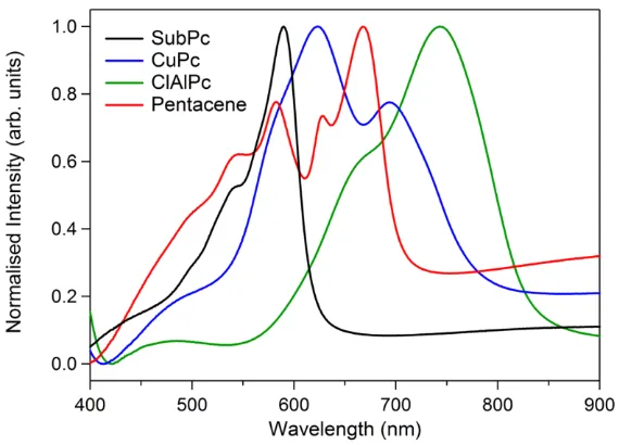
Figure 1.16: Normalized absorption spectra for thin films of four commonly used small
molecule organic donor materials: SubPc, CuPc, ClAlPc and Pentacene.69
1.7.3- Material 3- Electron Acceptor Material
In an OPV, the electron accepting material accepts electrons and transports holes to the
electron donor material. The fullerenes shown in Figure 1.17 are often used as electron
acceptors for OPV due to their high electron affinities, high electron mobilities, good
exciton diffusion lengths and absorption in the green region of the visible spectrum. Each
carbon in the C60 molecule is sp2 hybridised, with each atom forming one double and two
single bonds. Both PCBM and C60 undergo photo-induced polymerisation reactions upon
38
Figure 1.17: The chemical structures three common acceptor materials C60 (left), PCBM
(middle) and PC70BM (right).
C70 is another fullerene that can be used as a small molecule electron acceptor in
bilayer OPV devices. It has been shown to yield increased PCE in OPV cells when
compared to devices using C60 due to increased absorption and improved electron
transport. C70 based OPV are also found to be more stable,73 although C70 is much more
expensive to produce than C60.74 C60 and C70 are often derivatised to ensure solubility in
organic solvents for more facile processing (e.g. PCBM and PC70BM, Figure 1.17).70 As
such, C60 is usually used as the electron acceptor in evaporated small molecule OPVs,
with PCBM or PC70BM used in the solution processed BHJ OPVs. Polymeric acceptors
are less commonly used in OPVs because they often undergo large scale phase
segregation when blended with donor polymers, and consequently yield relatively poor
efficiencies in OPV devices.75
Al and Ca are the most commonly used materials for the top opaque electrode
39 depth here, although it is worthy to note that their main issue is susceptibility to
oxidation.
1.8 Window Electrodes for OPV
The core issue with transparent electrodes for OPVs is that the free electrons that impart
conductivity also interact strongly with light, reducing the transparency of the electrode.
Window electrodes for OPV devices must therefore be designed with this fundamental
problem in mind, as an increase in the conductivity of an electrode will often decrease its
transparency and vice versa; consequently a compromise must be achieved.
Window electrodes in OPV devices need to fulfil three important criteria. They
need to be optically transparent to let light into the device, electrically conductive to
allow the extraction of photogenerated charge carriers, and finally not so rough as to
undermine device shunt resistance due to filamentary short formation.76,77 The surface
energy, work function, cost, flexibility and long term stability are also important factors
for electrode materials for OPV fabrication. The chemical stability of electrode materials
is of importance, as PV modules are exposed to the elements and to significant heating in
sunlight, which can raise the temperature to values as high as 60 °C.78 A low surface
roughness is required due to the very thin active layer thicknesses utilised in OPV
devices. In practice, the window electrode RMS roughness needs to be ≤ 2 nms. The
window electrode material also has to be transparent right out to wavelengths of 950 nm,
to ensure the maximum amount of the solar spectrum is harvested. An electrode’s
transmission spectrum must be carefully considered, since for an OPV a low transparency
in the ultra-violet part of the solar spectrum can be advantageous, as many organic
40 An OPV’s series resistance (or internal cell resistance) can affect the efficiency
of the device drastically. The electrical conductivity of window electrodes is quantified in
terms of sheet resistance. A window electrode for an OPV must have a sheet resistance of
≤10 Ω sq-1
to ensure that a large drop in PCE is not observed when OPV cells are scaled
up to a large cell area for applications.46,79 These losses can be mitigated by using
transparent electrodes with higher conductivity.80 Thus highly conductive transparent
electrode materials are a prerequisite for the realisation of OPV technology industrially.
The leading window electrode materials for OPV are doped metal oxides, as
they provide a good compromise between transparency and sheet resistance. The metal
oxides utilised have wide band gaps and therefore offer a high degree of optical
transparency. These metal oxides are degenerately n-doped to increase the conductivity
by orders of magnitude. This doping can often be in concentrations as high as 10 atomic
%. Figure 1.18 illustrates this for the most commonly used OPV window electrode
material, indium-tin oxide (ITO) coated glass. The doping of the material preserves its
wide band gap whilst greatly increasing the conductivity as compared to the undoped
state.
41 ITO glass used for OPVs has a sheet resistance of 6-15 Ω sq-1 and a transparency
of 75-95% over the visible spectrum. ITO’s transparency and sheet resistance are a
function of the thickness; the sheet resistance and transparency decrease as the film
thickness is increased, with considerably lower transparencies at 6 Ω sq-1 (sheet
resistance suitable for application in OPVs) compared to the 15 Ω sq-1 normally used in
small area OPVs as shown in Figure 1.19.
Figure 1.19: Far-field transparency spectra of ITO glass at 6 Ω sq-1 (red) and 15 Ω sq-1
(black).
ITO does however have a number of drawbacks for applications in OPVs which
are discussed in Section 1.9.
1.9 ITO Problems
ITO coated glass is long established as the window electrode of choice for many
applications including displays, heat reflective glass and solid-state lighting including
OLEDs, where it is the industry standard.81 It is also the archetypal window electrode
material for OPVs, typically at a thickness of ~80 nm.82 Indium is produced mostly as a
42 scarcity of indium in the earth’s crust and the proliferation of flat screen displays mean
that indium and consequently ITO are expensive.57
There are also other problems with ITO glass for utility in OPVs: It has been
shown to account for 50-74% of the embodied energy in an OPV device,19,28 and its sheet
resistance (≈15 Ω sq-1) has been found to be a limiting factor for the PCE of OPVs
sufficiently large for practical applications.46,85,86 ITO is also meta-stable and is typically
deposited at temperatures above 250 °C to ensure optimum performance which makes it
poorly matched to the plastic substrates required for high speed roll-to-roll manufacture
of OPVs. When ITO films on plastic substrates are bent, cracks being to appear since ITO
is inherently brittle, resulting in much higher sheet resistance values.87 This is not the
case with ultra-thin metal films.85,86 The sheet resistance of ITO on flexible substrates
varies, but is invariably >35 Ω sq-1.85-87 Indium and tin have also been shown to diffuse
into the organic layers in OPVs.88 It is for these reasons that ITO has been described in
the literature as not a possible choice for scalable OPV.7
1.10 ITO Alternatives
It is widely recognized that the full cost advantage of OPVs over commercial silicon and
thin film photovoltaics can only be achieved if the electrode that couples light into the
device is based on inexpensive raw materials, involves simple, rapid fabrication processes
and is compatible with substrates that are sufficiently flexible for roll-to-roll fabrication
of devices.17,18,57 Due to the aforementioned issues many alternatives to ITO have been
proposed, some of which are described individually below. However, no clear leader has
yet emerged, since all of these alternative window electrodes have significant
43 materials, high surface roughness which increases the likelihood of parasitic current
shunting in a PV cell,76,77 or too high sheet resistance.76
1.10.1 Alternative Oxides
There has been significant research into other doped metal oxides, including indium
titanium oxide,83,89 and fluorine doped tin oxide (FTO).89 FTO is not often used in OPV
cells as it has large surface roughness as compared to ITO glass.89 This is not an issue for
DSSCs, where it is ubiquitous. Other metal oxides can possibly overcome some of the
issues associated with ITO, but not all of them as these materials will always be used in
films of 100s of nms in order to be sufficiently conductive for OPVs and will therefore
still be liable to crack upon bending. As these materials cannot be compatible with
flexible substrates, other alternatives must be sought for OPV.
1.10.2 Carbon Based Nanomaterials
The two main carbon based ITO alternatives are carbon nanotubes and graphene films.
Carbon nanotubes can produce films with comparable transparency to ITO glass.
However, the sheet resistance of these films is not low enough for large scale OPV.90 The
production methods for carbon nanotubes are also very energy intensive, and carbon
nanotube electrodes are intrinsically very rough, which is not ideal for OPVs.
Graphene monolayer and multilayer graphene are also being investigated as
potential transparent electrodes for OPV.91 Whilst graphene electrodes appear
theoretically tantalising, particularly once doped, high sheet resistance values of
≈ 200 Ω sq-1
at ≈ 80% transparency for fabricated films prohibit the use of graphene for
OPVs, where ≈10 Ω sq-1 is required.90 This problem is demonstrated by many of the
44 analogous ITO based devices.91 Graphene production methods are also energy intensive
and costly currently.
1.10.3 Conducting Polymers
Conductive polymers have undergone research as a material to replace ITO, however
they are too resistive to be used as a stand-alone replacement.92
1.10.4 Metal Nanowires
Metal nanowires have been suggested for replacement of ITO, including Cu nanowires.93
Metallic nanowires can be solution processed and have impressively low sheet resistance
and high transparency values.94 However, these electrodes have high RMS roughness,
which can cause shorting of the thin active layers in an OPV and have to be combined
with conductive polymers to smooth their surface.
1.10.5 Metal Grids
Solution processed silver grid electrodes for OPVs have received significant attention17 in
recent years. Evaporated metal grid electrodes have been achieved with sheet resistance
values as low as 2 Ω sq-1 at 90% transmission, which compares very favourably to ITO.95
This was achieved by electrospinning polymer fibres and then evaporating, or sputtering
electrode materials on top of them. The polymer grid is then dissolved using solvents.95
Whilst these values for transmission and sheet resistance are impressive, the metal
troughs are ≈80 nm high, which is comparable to the thickness of the semiconducting
layer in an OPV and shorting of devices is likely. It has been reported that for large area
printed OPVs fabricated on metal grid electrodes with comparable roughness, the short
circuiting of devices is an issue.96 The complexity of the fabrication process may also
45
1.10.6 Ultra-thin metal films
In recent years there has been renewed interest in both planar59,86 and patterned97
ultra-thin (<10 nm) metal films, as they provide both ideal model electrodes for laboratory
testing and offer the prospect of replacing ITO glass electrodes in OPVs. Issues with
robustness, transparency and resistivity have prevented the widespread utilisation, as
films of the most conductive metals are typically discontinuous at a thickness low enough
to be highly transparent. In principle, ultra-thin metal films could yield the required
characteristics to replace ITO films, although this has not yet been realised. Metals often
employed for this purpose include Au, Ag and Cu. Au is often used for laboratory use,
but may be too costly to implement on a large scale. Ag has the advantages of the highest
conductivity amongst metals and a low refractive index in the visible region.98 However,
both Au and Ag are expensive. Cu is relatively inexpensive; about 100 times cheaper than
Ag and 5000 times cheaper than Au.93 Cu is already widely used in the electronics
industry.98 It has comparable conductivity to Ag, and better conductivity than Al or Au.96
The primary obstacle to the use of Cu is the susceptibility to oxidation, which in the
context of an ultra-thin film is a serious problem.
Many ultra-thin metal films have been fabricated for use as electrodes in organic
electronics. These include both planar and nanostructured Au, Ag and Cu electrodes,86,97
Ag/Cu bilayers,98 and Ag electrodes seeded with Cu.98 If metal films are too thin, (i.e.
below the percolation thickness) they will remain as discontinuous island like structures,
causing scattering and a reduced transparency, and an increased sheet resistance.99 The
percolation thickness will vary depending on the metal, the deposition method and the
46 Finally, it is important to note that reduced transparency of the window electrode
in an OPV does not always lead to a reduced absorption in the organic semiconductor.
The increased reflection can create a resonant cavity between the window and back
electrodes, resulting in increased light harvesting.82,85
Metal oxides are useful in OPV devices as charge extraction interlayers, but also
useful for refractive index matching, thus improving ultra-thin metal film transparencies.
They will be discussed in Section 1.12.
1.12 Metal Oxides in OPVs
Metal oxide charge extraction layers are often used in OPVs between the electrodes and
the photo-active layer to improve device PCE and lifetimes. Metal oxides with low work
functions (e.g. ZnO, TiO2) and high work functions (e.g. WO3, MoO3, NiOx) are
available, with some having n-type (e.g. ZnO) and some having p-type (e.g. NiOx)
characteristics due to intrinsic defects. High work function metal oxides are used as hole
extracting interlayers in OPVs, and low work function oxides are used as electron
extracting interlayers in which context they serve to improve alignment between the
electrode Fermi level and the relevant frontier molecular orbital in the adjacent organic
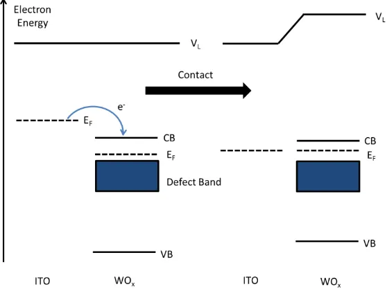
semiconductor as illustrated in Figure 1.20. Consequently when these oxides are used in
an OPV they typically increase the built in field across the organic layers, resulting in a
47
Figure 1.20: Energy level diagram depicting Fermi level alignment at the interface
between ITO and WOx.
Metal oxides can be vacuum or solution processed and the chemical potential
can be tuned by altering the amount of oxidation via changes to its deposition method,
thus changing the work function.101 Introducing more oxygen defects into the structure
reduces its chemical potential and work function, since the oxygen defects serve as n type
dopants.102 Metal contacts can affect an oxide’s chemical and electronic properties within
the first few nms of the contact, as a result of charge transfer or doping of the oxide by
the metal.102 For example, MoO3 becomes semi-metallic near contacts, reducing the work
function for films less than 10 nm.102 Interfacial chemical reactions between metal oxides
and organics have been shown to reduce charge transport barriers across interfaces,103 and
so metal oxides have widely used in organic electronics.104
Metal oxides are also used as optical spacers in OPVs to maximise light
[image:48.595.190.469.65.280.2]48 large charge carrier mobility, with materials like aluminium doped zinc oxide and
titanium dioxide often being used. Optical spacer layers maximise the light intensity in
certain areas of the cell, and so can be used to improve the short circuit current. They are
also used to prevent diffusion metal ions from the ITO electrode in OPVs.105
Tungsten trioxide (WO3) is a metal oxide that is widely used in electrochromic
devices, since its transparency is altered drastically when ions are injected into the
material.106 Typically Li, Na or H are used as dopants in WO3-x in photochromic devices.
Cu can also be used,32 although Cu doped WO3-x has not been utilized previously in
OPVs as a charge extraction material. The photochromic properties of Cu doped tungsten
oxide are very complex and not completely understood by the scientific community.107
Copper has also been shown to alloy with MoO3 and diffuse through MoO3 films. 102 This
diffusion of Cu into metal oxides has been previously viewed as an issue.108
Thin films of stoichiometric WO3 are transparent to most visible wavelengths
with a slightly yellow tint for very thin films,109 and a yellow/green colour in the bulk.107
The transparency of tungsten oxide has been shown to change upon UV irradiation.107
The band gap depends on the crystallinity of the sample, and ranges from 2.6-3.3eV.109,110
Evaporated WO3 has a work function of 6.5 eV, an electron affinity of 6.7 eV and an
ionisation potential of 9.8 eV,111 although the work function has been reported to be as
low as 4.9eV.99 The chemical, electronic and optical properties of tungsten oxide films
can vary hugely with different deposition techniques.112 Tungsten oxide has been used in
OPVs to increase the transparency of ultra-thin metal films87 and is suited for this role
due to its high refractive index.109 However, if the tungsten oxide interlayers used are too
thick, the series resistance of the device increases, and this leads to a reduced PCE, so a
49 MoO3 has similar properties to WO3, is widely used in OPVs as a hole transport
layer, is highly n- type doped and facilitates charge transport via the conduction band.113
With WO3 having a very similar ionisation potential, work function and electron affinity
to MoO3,113 its use as a hole transport layer is promising. It has been shown for MoO3
that thick (≈100 nm) layers in devices inhibit performance, but this can be overcome by
doping with metals.114 This allows the use of thicker spacers layers to maximise
absorption within an OPV device.
1.13 Plasmonics
In addition to metal oxides, another method of increasing the viability of ultra-thin metal
films as window electrodes for OPVs is plasmon enhanced absorption, which will now be
introduced.
Plasmonics is an active area of research for communications,115 sensing,116 and
more recently OLEDs117 and PVs.118 A surface plasmon resonance (SPR) is the resonant
response of free electrons in a conductor to incident light. This can be a local effect
confined to a nanoparticle, or aperture in a metal film, known as a localised surface
plasmon resonance (LSPR), or a propagating excitation known as a surface plasmon
polariton (SPP). These surface excitations result in a strong enhancement of the local
optical field. A schematic illustration of the excitation of LSPRs in a metal nanoparticle is
shown in Figure 1.21. The nanoparticle diameter is much smaller than the wavelength of
the incident light and the free electrons in the nanoparticle oscillate with the change of
50
Figure 1.21: LSPR induced in nanoparticles by coupling with visible light.
Much like nanoparticles, sub-wavelength holes in a metal film couple strongly
with incident light, exciting SPRs that are located at the site of the aperture. LSPRs
associated with an aperture in a film can leak into the surrounding metal film forming
propagating SPPs, as shown in Figure 1.22. This is an example of coupling between
localised and propagating surface plasmonic excitations.
Figure 1.22: Light coupled into a metal film via an aperture.
The onset wavelengths for surface plasmon excitation in Ag, Au and Cu are
~320, 540 and 590 nm respectively;115 and so the coinage metals are all plasmon active in