Abstract—Photonic network-on-chip (PNoC) has emerged as
a feasible solution for new multi core processor systems to avoid the limitations of power and bandwidth density of traditional electrical networks. However, it is inevitable that the photonic devices have high sensitivity to the temperature such as microring resonator which is widely used on NoCs. As the temperature is increased or decreased, wavelength shift is generated. In order to resolve that problem, an off-line task mapping based on the microring thermal perception is proposed in this paper. This scheme maps the tasks having high power consumption to the peripheral core before the application is executed, while the low power tasks are mapped first to the core of the light node that significantly decrease temperature of the optical node. The simulation results show that in a group of practical applications compared with the method based on shortest path mapping and our proposed scheme in 8×8×2 three-dimensional mesh optical NoC, later mapping algorithm significantly reduce temperature of the optical node from 1K to 2K.
Index Terms—task mapping, microring perception, PNoC,
thermal balance
I. INTRODUCTION
ith the increasing limitations of transistors that can be integrated in a single-core chip, the proposed multi-core processor helps achieve high-performance parallel processing with lower frequency costs. The network-on-chip (NoC) is now recognized as emerging on-chip communication architecture proposed by the industry in place of traditional multi-core processors [1]. However, the on-chip network of electrical interconnects has obvious drawbacks in communication bandwidth and power consumption and if the chip structure is to be passed through a pure optical network, it also affects the stability of the Manuscript received July 2, 2018. Revised July 25, 2018. This work was supported in part by the National Natural Science Foundation of China (No. 61774086, No. 61376025) and the Natural Science Foundation of Jiangsu Province (BK20160806).
X. GUAN is with the College of Electronic and Information Engineering, Nanjing University of Aeronautics and Astronautics, Nanjing, 211106, China. (email: [email protected]).
N. WU is with the College of Electronic and Information Engineering, Nanjing University of Aeronautics and Astronautics, Nanjing, 210016, China ([email protected]).
F. GE is with the College of Electronic and Information Engineering, Nanjing University of Aeronautics and Astronautics, Nanjing, 210016, China ([email protected]).
G. YAN is with the College of Electronic and Information Engineering, Nanjing University of Aeronautics and Astronautics, Nanjing, 211106, China, and with the College of Mathematics, Physics and Information Engineering, Anhui Science and Technology University, Fengyang, 233100, China.
overall communications. Therefore, an optical networks-on-chip communication architecture is proposed. Compared with the traditional pure electrical interconnect architecture, optical networks-on-chip can significantly increase the bandwidth density, which provide low power consumption and communication delay.
The optical-electrical interconnect technology helps to build a low-diameter interconnect network that reduces the difference in access delays of on-chip nodes and reduces communication power of many-core systems [6-10]. Based on wavelength division multiplexing, the existing optical-electrical interconnect technology is mainly divided into two categories: circuit-switched and optical on-chip network. Circuit switched network needs to control the signal steering in the optical router through the parallel electronic control network, so that resource utilization rate of the network is reduced and the communication speed of the optical link is also limited. Only when the amount of transmitted data is in the order of 1 KB or more in this way, the extra overhead caused by link establishment and release can be offset. An on-chip optical network on account of wavelength division multiplexing uses a passive optical switch to route according to the wavelength of optical information. Optical signals can be transmitted without the need for optical signals or optical signal buffers. For resource reservation requirements, the intermediate nodes are eliminated from the light, which can make better use of the advantages of high-speed and low loss optical interconnection. In addition, the resource reservation has become a popular trend in optical network research.
The thermal sensitivity of the optical link is a problem that needs to be resolved in optical networks based on wavelength division multiplexing technology. The thermal stability control of optical link is mainly reflected in temperature control of the microring resonator. The microring resonator is a basic component of an optical link, which provides signal modulation at transmitter, light deflection during transmission and optical filtering at receiver end. However, microring resonators are very sensitive to temperature fluctuations (thermal temperature coefficient is about 110pm/K), that make optical links such as optical modulation, optical deflection and optical filtering malfunction, when the on-chip temperature changes. Some literatures have evaluated the thermal stability of 2D on-chip optical network through experimental methods. Without any thermal management measures average communication error rate of the entire network is more than 10-1. In order to reduce the thermal effects in optical NoC, many thermal management techniques have been proposed such as OS-based workload migration and DVFS (Dynamic Voltage
An Off-line Task Mapping Method based on
Microring Perception Thermal Balance
Xiaoyu Guan, Ning Wu, Fen Ge, and Gaizhen Yan
and Frequency Scaling) to reduce the on-chip temperature gradient. In addition, microring resonators and athermal microring resonators with small temperature dependence can be made by thermal properties of the polymer materials. However, this scheme has more requirements on the process. In addition, some efforts have been made to overcome thermal challenges in optical NoCs at a system level perspective. Author proposed a thermal sensing method to design an optical NoCs with distributed CMOS-compatible VCSELs (vertical cavity surface-emitting lasers) through analysis in [16]. Simulation of thermal effects in optical NoCs and several low-temperature sensitive technologies are proposed in [14], [15]. A system-level active thread migration technology and a device-level heat island framework to alleviate the thermal problem in optical NoC is published in [17].
Thermal compensation using a heating loop and a closed-loop control circuit is a mature thermal stability control method in industry. The resulting power consumption is called thermal tuning power consumption. Since the heating ring cannot dissipate heat, whether the microring is red-shifted or blue-shifted requires a heating operation. When the thermally stable operating range is 20K, the tuning power consumption of a single microring can reach 20μW. That makes the interconnection system available to receive constraints and increase power consumption overhead. In fact, the microrings in same optical node have similar temperature loop mirrors and same temperature characteristics. Therefore, the offline task mapping temperature control scheme is used to uniformly tune all the microrings at the same optical node to avoid additional heating loop temperature tuning power.
II. THERMAL-SENSITIVE DESIGN AND TASK MAPPING ALGORITHM REVIEW STAGE
In this section, the heat-sensitive characteristics of the microring resonator and the effects of temperature changes on the wavelength are analyzed. Based on optical thermal model, thermal effect in optical NoCs is described from a system level perspective. Moreover, an off-line task mapping algorithm based on thermal sensitivity for real applications is proposed for 3D mesh optical NoCs.
A. 3D mesh-based optical NoC architecture
Compared with electrical NoCs, photonic NoCs is a new technology as it has low power consumption and higher bandwidth. So far, the industry has proposed several high performance PNoC topologies, such as mesh [2], [4], 3D- mesh [5] [11], crossbar [3], torus [12] and clos [13]. Our main focus is on MRR’s and waveguides.
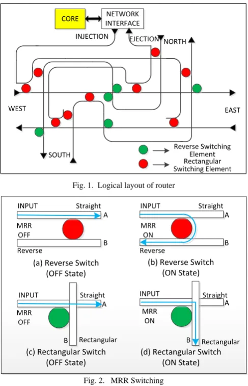
As shown in Fig. 1, the routing structure of PNoC is a 5×5 optical router. One of the router ports is connected to the core while the other four ports are connected to the neighboring routers. The key device in the router is MRR(microring resonator). MRR is an annular coil waveguide which controls the propagation of optical signals. It is used as a basic switching element in photonic routers.
The switching mechanism of MRR is shown in Fig. 2. As shown in Fig. 2a and Fig. 2c, MRR allows optical signals to be transmitted straight through the input port without any
offsets in the closed state. When in open state (Fig. 2b and Fig.2d), MRR couples the optical signal of the waveguide wavelength from the waveguide A to the waveguide B. For reverse handover, two parallel waveguides are shown in Fig. 2b. As shown in Fig. 2d, the two waveguides are placed into rectangular switches with a 90 degree angle.
CORE NETWORK
INTERFACE
INJECTION EJECTION NORTH
EAST WEST
SOUTH
[image:2.595.305.549.127.506.2]Reverse Switching Element Rectangular Switching Element
Fig. 1. Logical layout of router
MRR OFF
INPUT Straight INPUT
INPUT INPUT
Straight
Straight Straight
Reverse
Rectangular
Reverse
Rectangular A
B
A
B
B B
A A
(a) Reverse Switch (OFF State)
MRR OFF
MRR ON
MRR ON
(b) Reverse Switch (ON State)
(c) Rectangular Switch (OFF State)
(d) Rectangular Switch (ON State)
Fig. 2. MRR Switching
Optical NoCs transmit data and control information between processor core and memory through optical signal. In different Optical NoCs architectures, optical signals are transmitted through different optical links. Although the structure is diverse, the optical links in Optical NoCs are usually made up of optical paths, optical transmitters and optical receivers (shown on Fig. 3). The laser source can convert electrical signals into optical signals by directly modulating the driving current of VCSEL [29] or using optical modulators. VCSEL is assumed as the source of the PNoC laser and use 3D integration technology to connect the underlying CMOS drive circuit through VCSEL through TSVs (through silicon via).
studied.
Ele
ct
ro
n
ic
d
o
m
ain
1
Ele
ct
ro
n
ic
d
o
m
ain
2
VCSEL
MR
MR
MR
...
Photod ectector
Optical link
Switching stage 1
Switching stage 2
Switching stage N Optical
transmitter
Optical receiver
[image:3.595.52.274.53.189.2]Optical path
Fig. 3. MRR Switching
B. Thermal Sensitivity of Microring Resonators
For a microring resonator, its resonant wavelength generally depends on the geometric parameters of the microring resonator, as shown in equation (1).
n
effL
m
(1) Here m is an integer representing the resonant mode, Lrepresents the circumference of the microring resonator and
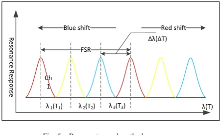
neff represents the optical modulus-dependent coefficient depending on temperature. neff has an approximately linear temperature-sensitive characteristic, so the microring wavelength can also be considered to change linearly with temperature. At the same time, the frequency response characteristics of microring resonators are periodic, as shown in Fig. 5.
The distance between adjacent peaks of the continuous resonance curve is called free spectral range of the microring resonator. Different channel wavelengths should be selected within the same FSR(Free Spectral Range). The number of wavelengths used in the interconnection system is nλ, and the sensitivity of the microring wavelength is k ,then allowable temperature gradient within the same FSR is:
T
FSR
k n
(2)When the temperature difference of the whole piece or the temperature change exceeds this value, a thermal stability control strategy needs to be introduced to avoid crosstalk between channels. The traditional method is to use a heating ring. When the temperature is reduced and the wavelength is blue shifted, the microring is heated back to the original tuning point. When the temperature is raised and the wavelength is red shifted, the microring is heated through heating. A resonant wavelength in the FSR leads to a larger microring tuning overhead. In this topic, the system level thermal stability control method is adopted to improve the temperature environment of the microring by reasonably guiding and distributing the heat generated by the functional components themselves, thereby a microring tuning scheme with low power consumption is formed.
The temperature variation of the optical node N can be expressed as:
ek
R
N k
T
P
(3) Pk is composed of four parts: Pcore, Pcomm, Pcache, and Pheater, which respectively calculate the power consumption for the processor. The circuit is powered by the unit communication power, cache read/write power consumption and heatingloop tuning power consumption.
Laser Source
ON ON/OFF
ON ON
(d)Modulator
(a)Switch
(c)Demultiplexer (b)Multiplexer
[image:3.595.309.541.60.180.2]
Fig. 4. Representative schematics of ring-resonator building blocks.
FSR
Ch 1
Blue shift Red shift
λ 1(T1) λ 2(T2) λ 3(T3)
∆λ(∆T)
λ(T)
R
es
o
n
an
ce
R
es
p
o
n
se
Fig. 5. Resonant wavelength change curve
In view of adjusting communication power consumption of individual routing units, it may lead to route congestion, thus forming bandwidth bottleneck of the entire communication system. This article will no longer use communication power as an adjustment object.
With a rise in temperature, rings will not resonate at the intended frequency. Modulators, switches, multiplexers, and demultiplexers will produce erro-neous outputs if thermal shifts are not addressed. Fig. 4 shows several scenarios showing the intended and the actual outputs when a ring fails to resonate at the intended frequency due to a rise in temperature.
C. Microring-aware thermal-balanced task mapping
Considering the thermal balance problem, the background problem of task mapping algorithm design becomes more complex. Constraints of algorithm design include not only resource limitations but also threshold temperature or TDP power constraint caused by thermal effects. The optimization goal is no longer simply to pursue the communication distance, the delay as small as possible, the system throughput is as large as possible. At the same time, optimization of the peak temperature distribution is considered to avoid hot spots and realize heat balance and so on.
Mapping tasks to NoC systems is multiple to multiple mapping problems where each task needs to be determined. The position of processing unit is placed. Different allocation schemes may have different effects on performance indicators, such as energy consumption, fault tolerance and thermal equilibrium.
Before the task runs, the loop aware thermal balance task mapping is implemented first. Let the microring operates at the reference temperature of the tuning frequency as T0 and
[image:3.595.313.538.207.345.2]adjacent FSR is ∆T. When the temperature distribution of the optical node satisfies Equation (4), each microring can work in stable condition.
T
NT
0
k T
(4)Task mapping follows the steps below:
1)Calculate the power consumption P0 and ∆P corresponding to T0 and ∆T based on equation (3).
2)Estimate the deviation of calculated power Pi and all tasks, ie:
0
(
)
i i
P
P
P
k P
(5) 3)The task with smallest power consumption deviation is first mapped to the processor node having same plane coordinates as the optical node. That means d-0 mapping shown in Fig. 6 is completed. After that, d-1 mapping is performed so that the total power consumption deviations of all nodes in the mapping area of each optical node d-1 are approximately equal and tends to 0.the formula is Equation (6).1_ 1 2_ 1 L_ 1
k k k
k M d k M d k M d
P P P
(6) 4)By analogy, the light nodes radiate outward until all task mappings are completed.
The task map is shown in Fig. 6. Tasks with the least power consumption from the core map at the bottom of the optical node are scaled out in order until the mapping of all tasks is completed.
d-0 Mapping
d-1 Mapping
d-2 Mapping
[image:4.595.315.535.181.464.2]Optical Node
Fig. 6.Mapping distribution
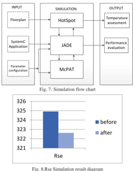
III. SIMULATIONRESULTSANDCOMPARISONS Optimized and un-optimized temperature conditions of 3Dmesh topology is evaluated through the mapping algorithm. The cycle precision simulator on account of SystemC is developed for network simulation of optical NoC based on 3D-mesh. Network simulation is carried out in several practical applications including FPPPP, H263E, H264DH, H26DL, ROBOT, SAMPLE and SPARSE. For each application, traffic information is used to simulate the temperature distribution of McPAT chip [21] and HotSpot [22]. The specific simulation process is shown in Fig. 7. Laser wavelength and resonant wavelength of microring resonators are 1550nm at room temperature.
A. The effectiveness of the mapping algorithm
In the initial un-optimized mapping, the original mapping is based on the shortest path to map. The simulated task power consumption is introduced into the HotSpot to generate the temperature situation. Then we remap the task through our optimization algorithm, and we can also get a new temperature condition by performing the above
operation. Ideally, our optimized temperature is better than the one without optimization. Actually as shown in Fig. 8, the task at this time is chosen as the basic task and core steady-state temperature before the algorithm is 324.915K. When the core steady temperature below the light node after our algorithm is changed, the core steady temperature is 322.633K and temperature of core at the bottom of time node has an obvious lower temperature. The proposed optimization algorithm has obvious advantages for the thermal sensing of microring.
Floorplan
SystemC Application
Parameter configuration
INPUT
HotSpot
JADE
McPAT
SIMULATION OUTPUT
Temperature assessment
Performance evaluation
Fig. 7.Simulation flow chart
321 322 323 324 325 326
Rse
before
after
Fig. 8.Rse Simulation result diagram
B. Other task and Network performance
A task with a large number of tasks is selected. The proposed mapping algorithm has much impact on the core temperature below the optical node. The temperature situation is shown in Fig. 9.
330 335 340 345 350 355
before
[image:4.595.86.253.388.511.2]after
Fig. 9.Multi application simulation result diagram
IV. CONCLUSION
[image:4.595.312.537.540.649.2]core temperature below the optical node is generally reduced by 1K to 2K.
REFERENCES
[1] W. Dally and B. Towles, “Route packets, not wires: on-chip interconnec-tion networks,” in Proc. Design Automation Conf., 2001, pp. 684–689.
[2] A. Shacham, K. Bergman, and L.P. Carloni, Photonic networks-on-chip for future generations of chip multiprocessors, IEEE Trans. Comput.57(9), 12461260 (2008).
[3] H.X. Gu, K.H. Mo, J. Xu, and W. Zhang, A low-power low-cost optical router for optical networks-on-chip in multiprocessor systems-on-chip, 2009 IEEE Computer Society Annual Symposium on VlSI, 1924 (2009).
[4] D. Dang, Biplab Patra, Rabi Mahapatra, Martin Fiers, Mode-Division- Multiplexed Photonic Router for High Performance Network-on-Chip, 28th IEEE VLSID 2015, (2015), pp. 111-116.
[5] D. Dang, Biplab Patra, Rabi Mahapatra, A 2-layer Laser Multiplexed Photonic Network-on-Chip, 16th IEEE ISQED 2015, pp. 397-401. [6] S. Bahirat and S. Pasricha, “UC-PHOTON: A novel hybrid photonic
network-on-chip for multiple use-case applications,” in 11th Int. Symp.Quality Electronic Design, 2010, pp. 721–729.
[7] K. H. Mo, Y. Ye, X. Wu, W. Zhang, W. Liu, and J. Xu, “A hierarchical hybrid optical-electronic network-on-chip,” in IEEE Computer Society Annual Symp. VLSI, July 2010, pp. 327–332.
[8] L. Ramini, A. Ghiribaldi, P. Grani, S. Bartolini, H. T. Fankem, and D. Bertozzi, “Assessing the energy break-even point between an optical noc architecture and an aggressive electronic baseline,” in 2014 Design,Automation Test in Europe Conference Exhibition (DATE), March 2014,pp. 1–6.
[9] S. Werner, J. Navaridas, and M. Lujn, “Amon: An advanced mesh- like optical noc,” in 2015 IEEE 23rd Annual Symposium on High- Performance Interconnects, Aug 2015, pp. 52–59.
[10] S. Faralli, N. Andriolli, F. Gambini, P. Pintus, G. Preve, M. Chiesa, R. Ortuno, O. Liboiron-Ladouceur, and I. Cerutti, “Bidirectional trans- missions in a ring-based packaged optical noc with 12 add-drop mi- crorings,” in 2016 IEEE Photonics Conference (IPC), Oct 2016, pp.621–622.
[11] D. Dang, Biplab Patra, Rabi Mahapatra, A Multilayered Design Approach for Efficient Hybrid 3D Photonic Network-on-Chip, 25th ACM/SIGDA GLSVLSI 2015, pp. 121-126.
[12] C. Batten et al. Building manycore processor-to-DRAM networks with monolithic silicon photonics, High-Performance Interconnects, Symposium on, pp. 2130, 16th IEEE Symposium on High Performance Interconnects, (2008).
[13] A. Joshi, C. Batten, Y.J. Kwon, S. Beamer, I. Shamim, K. Asanovic, and V. Stojanovic, Silicon-photonic clos networks for global on-chip communication, 2009 3rd Acm/Ieee International Symposium on Networks-on-Chip, 124-133 (2009).
[14] Y. Ye, J. Xu, X. Wu, W. Zhang, X. Wang, M. Nikdast, Z. Wang, and W. Liu, “System-level modeling and analysis of thermal effects in optical networks-on-chip,” Very Large Scale Integration (VLSI) Systems, IEEE,Transactions on, vol. PP, no. 99, pp. 1–14, 2012. [15] Y. Ye, Z. Wang, P. Yang, J. Xu, X. Wu, X. Wang, M. Nikdast, Z.
Wang,and L. H. K. Duong, “System-level modeling and analysis of thermal effects in wdm-based optical networks-on-chip,” IEEE Transactions on Computer-Aided Design of Integrated Circuits and Systems, vol. 33,no. 11, pp. 1718–1731, Nov 2014.
[16] H. Li, A. Fourmigue, S. L. Beux, X. Letartre, I. O’Connor, and G. Nico- lescu, “Thermal aware design method for vcsel-based on-chip optical interconnect,” in 2015 Design, Automation Test in Europe Conference Exhibition (DATE), March 2015, pp. 1120–1125.
[17] D. Dang, S. V. R. Chittamuru, R. Mahapatra, and S. Pasricha, “Islands of heaters: A novel thermal management framework for photonic nocs,” in 2017 22nd Asia and South Pacific Design Automation Conference (ASP-DAC), Jan 2017, pp. 306–311.
[18] B. Feero and P. Pande, “Networks-on-chip in a three-dimensional environment: A performance evaluation,” Computers, IEEE Transactions on, vol. 58, no. 1, pp. 32–45, Jan. 2009.
[19] H. Gu and J. Xu, “Design of 3D optical network on chip,” in Photonics and Optoelectronics, Symposium on, Aug. 2009, pp. 1–4.
[20] Y. Ye, J. Xu, B. Huang, X. Wu, W. Zhang, X. Wang, M. Nikdast,Z. Wang, W. Liu, and Z. Wang, “3-d mesh-based optical network-on-chip for multiprocessor system-on-chip,” IEEE Transactions on Computer-Aided Design of Integrated Circuits and Systems, vol. 32, no. 4, pp.584–596, April 2013.
[21] S. Li, J. H. Ahn, R. D. Strong, J. B. Brockman, D. M. Tullsen,and N. P. Jouppi, “Mcpat: An integrated power, area, and timing modeling framework for multicore and manycore architectures,” in 2009 42nd Annual IEEE/ACM International Symposium on Microarchitecture (MICRO), Dec 2009, pp. 469–480.