Atmospheric Pressure Plasma Treatment and Non-Flux Lead-Free-Soldering
of Cu Wire and Strand
Tomohiro Okumura
1, Mitsuo Saitoh
1, Kazutaka Nishikawa
1,
Akio Furusawa
2and Kenichiro Suetsugu
21Production Core Engineering Laboratory, Matsushita Electric (Panasonic), Kadoma 571-8502, Japan 2Jisso Core Engineering Laboratory, Matsushita Electric (Panasonic), Kadoma 571-8502, Japan
There has been an intensive effort in the industries in recent years to replace leaded solder with lead-free process in order to minimize the emission of toxic materials. However, leaded solder is still used in many cases where no alternative lead-free process is currently available. Leaded soldering of the wire terminals is one of the worst examples as it causes cross contamination of lead into the lead-free solder bath during the successive process. To avoid this problem, it is important to develop a new process of successfully removing polymer film coated on a copper wire. We have investigated the use of atmospheric pressure plasma as a solution for the polymer removal in conjunction with lead-free solder plating. The atmospheric plasma technology has some unique advantages compared with the conventional low pressure plasma processes such as low cost operation and high speed processing as the chemical reaction tends to be more enhanced at higher pressure. An atmospheric micro-plasma source was thus developed for this purpose and its high etching rate of more than 100mm/min with fluorine gas mixture was demonstrated. Furthermore, it was found that the copper wires processed by this plasma could be readily plated with lead-free solder at low temperature of 250C without any use of fluxes even at 168 h after removing the polymer film.
(Received November 10, 2005; Accepted February 2, 2006; Published March 15, 2006)
Keywords: polymer removal, polyester-imide, coil terminals, atmospheric pressure plasma, plasma etching, lead-free, solder, plating, flux-free
1. Introduction
Environmental safety is one of the most important areas of improvement in the industry at present and the use of lead-free solder is strongly encouraged. Lead-lead-free flow and reflow processing techniques have already been applied in manu-facturing.1)However, we still have a number of sources of lead contamination, one of which is the dissolution of lead in a solder bath during the wave soldering process. The source of the lead contamination in this case is the plated wire terminals using leaded solder. However, an alternative lead-free plating process for this type of application has not been identified. The commonly used leaded process is to remove the polymer film on the wire terminals and plate them simultaneously by dipping them into a molten leaded solder at approximately 310 to 380C.
The conventional process described above cannot be applied to the present lead-free solder plating as it causes an encroachment of a copper wire. Copper dissolves into the molten solder once the polymer film on its surface is removed. This problem is caused by both chemical reaction and diffusion. The known chemical reaction is the formation of metallic compounds such as Cu6Sn5and Cu3Sn resulting from the direct contact of copper with tin compounds. The encroachment tends to be pronounced on Sn–Ag–Cu solders as it can lead to a reduction of a wire diameter by nearly 50%.2) This problem becomes very severe for a fine wire whose diameter is 0.3 mm or less. It is therefore very important to establish the method of removing the polymer film from a copper wire that is compatible with the lead-free plating process.
There are many conventional methods used for polymer removal such as mechanical grinding, laser irradiation and chemical wet etching. Mechanical grinding has a risk of excessive removal resulting in shrinkage of the wire diameter. Laser irradiation method tends to leave polymer
residue on the wire surface. Chemical wet etching requires the toxic liquid at high temperature. Furthermore, the mechanical grinding and the laser irradiation methods necessitate the use of the flux prior to the soldering process. The flux removes oxides from the surface of the copper wire to improve its wettability. However, the residue of the flux may cause serious problems such as corrosion, electric leakage and migration of materials in a later stage. Most fluxes contain VOCs (Volatile Organic Compounds) that may contribute to photochemical air pollution. There are a few VOC-free fluxes developed so far,3) but the flux-free soldering is more desirable to eliminate any potential issues associated with this treatment.
We have thus decided to study a polymer removal process on wire terminals of coils using atmospheric pressure plasma and investigated its compatibility with the lead-free solder plating. Plasma etching technique has been widely used as a vacuum process in semiconductor manufacturing, but its cost would be too high to do low cost fabrication such as plating coil terminals. Atmospheric plasma technology has made considerable progress in recent years and it offers many advantages including low cost operation and high speed processing. A few examples of the atmospheric pressure micro-plasma etching were studied in the past.4–7)Plasma can be categorized into two types in general; equilibrium and non-equilibrium. In case of non-equilibrium plasma, al-though the temperature of electrons can be as high as tens of thousands degrees Celsius, the temperature of ions and neutral particles would still be as low as hundreds degrees Celsius. This suggests that the non-equilibrium plasma would have an advantage of effectively vaporizing the coated polymer on the copper wire with very little thermal damage to the metal surface, which is why we chose this approach. A reactive gas diluted by helium was used as a source gas for the plasma.
On the other hand, the use of ion beam treatment (Ar and
C3F8) on lead-free solder was previously reported as a method to improve the wettability of the metal surface.8,9) The samples were treated for 10 min by either Ar or C3F8ion beam. Ar beam treatment resulted in 24–48 h of wettability, while C3F8treatment gave over 96 h of wettability due to the formation of thick fluorinated layer on the Sn–Ag solder. However, the removal process of the polymer film was not considered as the improvement on wettability was the only purpose of this study. It should also be noted that our new method using the atmospheric plasma performs both the removal of the polymer and the improvement on wettability at the same time within ten and a few seconds.
This paper describes the structure of the micro-plasma source and explains the etching characteristics as a function of gas chemistry, process time and the location of wire in the plasma source. The plating performance on a single wire and a strand of wires is demonstrated with a lead-free solder. XPS (X-ray Photo electron Spectroscopy) analysis is also em-ployed to discuss the chemistry of the polymer etching reaction and the property of the surface states after polymer removal.
2. Experimental
2.1 Samples
We prepared 2 kinds of single wire samples; one is a copper wire of 150mmdiameter coated with 25mmpolymer film (200mmin total diameter) and the other is a copper wire of 190mmdiameter coated with 25mmpolymer film (240mm in total diameter). We also used a strand of 40 wires; each of which is a copper wire of 70mmdiameter coated with 25mm polymer film (120mmin total diameter). The material of the polymer was polyester-imide whose structural formula is shown in Fig. 1, where R and R0denote alkyl chains.
2.2 Atmospheric pressure plasma source composed of a fine ceramic tube
A schematic of the plasma source is shown in Fig. 2. The plasma source comprises a ceramic tube, a set of parallel plate upper and lower electrodes and a grounded metal case. The tube is sandwiched in between the two electrodes and has a gas inlet at one end, a gas outlet at the other end and the pedestals inside. Reactive gas mixture is supplied from the inlet, ionized within the tube and comes out from the gas outlet. A polymer coated copper wire is inserted from the opening of the gas outlet and is placed between the pedestals. The coated copper wire is suspended within the tube without touching its inner wall. The dimensions of the plasma source are as follows. G (gap between the electrodes) is 1 mm, L (length of the electrodes) is 5 mm, W (width of the air gap) is 5 mm and H (height of the air gap) is 0.7 mm. Gas mixture containing He, O2and CF4flows through the tube. Flow rate
of each gas is individually controlled by mass flow controllers. By applying radio frequency (13.56 MHz) volt-age to the upper electrode while keeping the lower one grounded, plasma can be generated inside the tube between the electrodes.
[image:2.595.310.539.73.422.2]2.3 Measurement
Figure 3 shows the set-up of the micrometer to measure the removal rate of the polymer film from the wire. Before and after etching polymer film the wire diameter was measured by using a wedge shape micrometer to obtain the removal rate of the polymer film. The wire diameter was determined by taking the average of the two values measured in orthogonal directions along A and B.
O
C
N
H
R
N
H
C
O
O
R’
O
n
Fig. 1 Structural formula of polyester-imide used to coat copper wires.
L=5mm
Metal case (grounded) Ceramic tube
Upper electrode
Gas inlet
Wire Gas outlet
Lower electrode
G=1mm
Pedestals Lower
electrode Ceramic
tube Upper
electrode
Wire Gas outlet
Cross sectional view
Front view
Ceramic tube
Pedestals W=5mm
H=0.7mm
Gas inlet
Metal case (grounded) (a)
(b)
(c)
Fig. 2 Atmospheric plasma source and its experimental setup; (a) config-uration of the atmospheric plasma source, (b) cross sectional view of the atmospheric plasma source, and (c) front view of the ceramic tube.
Direction B
Direction A
Micrometer
Copper wire
[image:2.595.304.551.483.570.2] [image:2.595.65.268.715.769.2]After polymer removal the wire was dipped into the Sn– 3.0Ag–0.5Cu solder bath for 3 s at 250C (32C higher than
the melting point of the solder) without using any fluxes. The length of the solder plated part was measured along the direction of the wire.
XPS analysis was carried out to examine the copper surface after the polymer removal. Copper plates with flat, smooth surface were prepared in stead of the copper wires for XPS analysis because it was difficult to perform the analysis on the round wires. Two different copper plates were examined; one was treated by HeþO2þCF4 plasma and the other by HeþH2plasma. The former represents a sample equivalent to the copper wire with its polymer removed. Deoxidization by HeþH2 plasma irradiation was used in order to reproduce a clean substrate surface that is equivalent to a mechanically grinded copper surface. The measurement was carried out at two points; the first was immediately after the plasma treatment and the second was after the plasma irradiation followed by the exposure in the atmosphere (23:52C,5010% humidity) for 168 h. Depth profiles
were obtained by using Ar sputtering.
Cross sectional observation of a plated strand of the wires was made by using SEM (Scanning Electron Microscope).
3. Results
3.1 Polymer removal process
An example of a polymer coated wire dipped into a molten
lead-free solder bath is shown in Fig. 4. As seen from the picture, the conventional plating process used in the leaded solder plating cannot be applied to the lead-free solder plating due to encroachment and dissolution of the copper into the molten solder.
We firstly examined the effect of atmospheric pressure plasma treatment using HeþO2gas mixture. The surface of the wire after plasma irradiation is shown in Fig. 5(a). The surface was covered with carbon-like residue and conse-quently the wire could not be plated with lead-free solder even by using a flux. Secondly, the effect of the plasma etching using HeþO2þCF4gas mixture was evaluated. In this case, the polymer was completely removed and the clean copper surface appeared as shown in Fig. 5(b). The wire was easily plated with lead-free solder without using any flux. It is worth noting here that CF4is an inexpensive material as it is commonly used in the semiconductor manufacturing in quantity.
Removed thickness of polymer film as a function of etching time is shown in Fig. 6. The experimental conditions were; the pressure = 100 kPa, radio frequency power = 120 W, He gas feed = 1000 sccm, O2 gas feed = 40 sccm and CF4 gas feed = 13.4 sccm. The diameter of the copper core of the wire was 150mmand the thickness of the polymer film was 25mm, which made the total diameter of the coated copper wire be 200mm. Removed thickness of the wire linearly increased from 5 to 15 s. The etching rate of the polymer film during this process was 104.0mm/min.
Re-Fig. 4 A microscope photo of a damaged polymer coated copper wire due to the reaction with a lead-free solder.
(a)
(b)
Fig. 5 Comparison of the etching performance between two different gas mixture. (a) HeþO2and (b) HeþO2þCF4.
0
5
10
15
20
25
30
0
5
10
15
20
25
Etching time,
t
/s
Removed thickness,
th
/
µ
m
initial thickness = 25µm
[image:3.595.49.290.73.213.2] [image:3.595.312.539.79.229.2] [image:3.595.101.497.275.406.2]moved thickness of the wire didn’t increase after 15 s, which means that the copper core did not undergo etching with over exposure in the plasma.
An image of plasma generation in the tube observed from the direction of the gas outlet is shown in Fig. 7. Locations A, B and C show the placement of the wire samples inside the tube. They were placed by 1.5 mm apart from each other inX
direction and by 0.1 mm apart in Y direction. Removed thickness of polymer film measured on the locations A, B and C at the etching time of 7.5 s was 14.3, 12.7 and 11.9mm respectively. The averaged thickness of removed polymer was 13:0mm9:2%. Good consistency in etching rate between the different locations indicated that the plasma density inside the tube was fairly uniform.
Cross sectional profile of a wire with its polymer coating removed in the middle is plotted in Fig. 8 in the direction of the wire length. The diameter of the coated copper wire was 240mmand the diameter of the copper core was 190mm. The right hand side of the axis is the upstream direction of the plasma and the left hand side is the downstream. The length of the wire portion in which the polymer was removed was 4.5 mm (the portion from 3 to 7.5 mm).
3.2 Plating process
A microscope picture of the polymer removed wire after dipped in a lead-free solder bath at 250C for 3 s is shown in
Fig. 9. No fluxes were used prior to the dipping process. The interval between the polymer removal and the dipping was 168 h (1 week), which means that, even after the sample was exposed in the atmosphere for 168 h, the copper wire can be successfully plated with the lead-free solder.
Figure 10 shows the comparison between plasma etching and mechanical grinding in terms of plated length of lead-free solder along the length of the copper wires. When the copper wires were dipped into the lead-free solder bath immediately after removing polymer film, the length of the plated portion on the wire was 5.6 mm for the plasma etching and 5.0 mm for the mechanical grinding. However once they were exposed in the atmosphere for 168 h after the removal of polymer film, the length of the plated portion for the mechanical grinding case decreased drastically down to 2.0 mm, although the length remained almost unchanged (5.0 mm) for the plasma etching case.
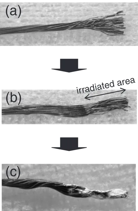
3.3 Application to a strand of wires as a batch process Lastly we attempted to apply this method to a strand of polymer coated copper wires as an example of a batch process. The sequence of the experiment is shown in Fig. 11. A strand of the wires was prepared by unraveling its one end (a) and irradiated with the atmospheric micro-plasma to remove the polymer film on each wire at once (b). After the plasma irradiation, the wires were twisted to resume a strand form and then plated with the lead-free solder (c). An SEM
Opening of the tube
1.5mm 1.5mm
A
B C
X Y
0.1mm 0.1mm
7mm
0.7mm
: Sample placement locations
Fig. 7 Image of the ceramic tube containing plasma observed from the direction of the gas outlet. Dispersion in removal rate among the three positions A, B and C was 103.6mm/min9.0%.
0 2 4 6 8 10
180 190 200 210 220 230 240 250
WIRE DIAMETER,
D
/
µ
m
downstream
78 µm/mm 34 µm/mm
upstream
Axial position along the length of wire, x/mm
Fig. 8 Cross sectional profile of a coated wire whose polymer film was removed in the middle.
5mm
Fig. 9 A microscope picture of a polymer removed wire after dipped in lead-free solder bath. The interval between the plasma irradiation and the dipping was 168 h (i.e.1 week).
0.0 1.0 2.0 3.0 4.0 5.0 6.0 7.0 8.0
0 168
Exposure time in the atmosphere,
t
ex/hPlated length of solder,
L
/mm
[image:4.595.50.291.74.182.2]Plasma etching Mechanical grinding
[image:4.595.308.548.74.180.2] [image:4.595.314.543.251.396.2] [image:4.595.55.283.263.420.2]image of the cross sectional view of a part of the strand after completing the batch process is shown in Fig. 12. A formation of alloy layer was observed in the interface between the copper wire and the solder. This alloy is assumed to consist of Cu3Sn and Cu6Sn5which have been identified as the typical alloys when using Sn–Ag–Cu solder.10)
4. Discussion
4.1 Polymer removal reaction
Polymer film is composed of C, O, H and N atoms. Therefore, the basic reaction in the plasma etching process can be expressed as follows.
PolymerþO!CO
2þCOþH2OþNO2þNO ð1Þ
Here O denotes an oxygen radical. All the generated
products in the right hand side of the eq. (1) are gaseous in the atmosphere, which would suggest that the polymer film would be removed in the presence of oxygen radicals. However the experimental results indicate that the reaction in the eq. (1) is incomplete to explain the actual removal process. As there was a large amount of carbon residue left on the wire surface when treated by HeþO2 plasma, one can expect that the removal rate of carbon in the eq. (1) would be very small. On the other hand, the successful polymer removal by using HeþO2þCF4gas mixture would suggest that a reaction of fluorine radical may contribute to the fast removal of the polymer by pulling hydrogen atoms out of the carbon chain. We assumed that fluorine radicals would react with hydrogen atoms to form HF molecules which would then help break the C–C bonding of the polymer body. The reaction assumed above can be expressed as follows.
PolymerþOþF!HFþCO
2
þCOþH2OþNO2þNO ð2Þ
Here F denotes a fluorine radical.
Good linearity of the removal rate as a function of time would indicate that the primary process of removing polymer film was a chemical reaction rather than a heat reaction, because the temperature rise during plasma irradiation didn’t raise the removal rate. It should also be noted that the unique plasma source with the ceramic tube and the narrow gap electrodes made it possible to achieve very high etching rate of the polymer at over 100mm/min as it was able to sustain high RF power without causing unstable arc discharge. Typical etching rate for polymer films in vacuum plasma is no more than 10mm/min. Furthermore, the selectivity of the plasma etching was also excellent. Once the polymer is etched away and the clean surface of copper appears, oxygen and fluorine radicals would both interact with copper. However, the removal process appeared to stop on the surface of the copper core in this case. The reason for the selective reaction can be attributed to high boiling points of both copper oxides and copper fluorides. The boiling points of CuF and Cu2O are 1100 and 1800C respectively.11)
In the upstream side of the tube, the slope of the etching rate profile is 78mm/mm which is very steep and in the downstream the slope is 34mm/mm which is less steep. This would indicate a difference in density of oxygen and fluorine radicals between the two locations. As the reactive radicals travel through the tube, they would undergo various processes such as quenching by collision, recombination and relaxation to reduce their number density, thus the etching rate gradually decreases along the direction of the gas flow.
The fact that the strand of copper wires was successfully treated would indicate that the atmospheric plasma can fill up
irradiated area
(a)
(b)
[image:5.595.50.288.71.434.2](c)
Fig. 11 A batch process applied for a strand of coated copper wires.
Lead-free solder
Copper wire
Copper wire
Alloy layer
[image:5.595.49.290.481.660.2]all the air gaps in the strand with radicals to achieve the uniform process on both the polymer removal and the surface treatment.
4.2 Analysis
XPS analysis was carried out to examine the difference in surface topology between plasma etching and mechanical grinding. Wide scan XPS results of copper surfaces imme-diately after plasma irradiation are shown in Fig. 13.
XPS depth profiles of copper surfaces in the case of Heþ H2 plasma treatment are shown in Fig. 14; (a) immediately after and (b) 168 h after plasma irradiation. HeþH2plasma irradiation deoxidized the sample surface to reveal clean surface of copper, but it underwent oxidization rapidly in the atmosphere to a depth of approximately 1 nm within several seconds. The measurement of Auger electron spectroscopy (AES) indicates that the oxidized layer was composed mainly of Cu2O in which the charge state of Cu atom is a plus one. After being exposed for 168 h in the air, the oxidized layer grew to 2 to 3 nm in thickness on the surface of the copper. AES results indicated that the components of the oxides were Cu2O and CuO and the uppermost surface layer was mostly CuO. These results clearly indicated that the oxidation process progressed over the 168 h.
XPS depth profiles of copper surfaces in the case of Heþ
O2þCF4 plasma treatment are shown in Fig. 15; (a) immediately after and (b) 168 h after plasma irradiation. HeþO2þCF4 plasma irradiation caused fluorination of copper surface to a depth of approximately 10 nm. The slope of each line in the profile changes at the depth of 5 nm, which suggests that fluorine atoms thermally diffused from the region within 5 nm to the deeper region up to 10 nm.
By comparing the total count of fluorine atoms (i.e. integration along the depth from the surface to the bulk substrate) between (a) and (b), the quantity of fluorine atoms appeared to be increased over the 168 h exposure in the atmosphere. A plausible interpretation of this phenomenon is as follows. CuO clusters are formed on top of CuF2layer and distributed over the surface. Those CuO clusters would cause double count of the fluorine atoms when the signals originated from the CuF2 layer travel through the CuO clusters. It should be noted that the depth profile of fluorine and its integration along the depth from 12 nm depth to the bottom in Fig. 15(b) roughly matches those in Fig. 15(a) from the surface to the bulk. This may suggest that the profile in Fig. 15(a) starting from the surface corresponds to the portion of the profile in Fig. 15(b) starting from 12 nm. Strength of chemical bonding of Cu–F and Cu–O is 413 kJ/ mol (4.3 eV) and 269 kJ/mol (2.8 eV) respectively,12)which would suggest that the substitution between oxygen and
0 200 400 600 800 1000 1200 1400 0
200 400 600 800 1000 1200 1400
(b)
(a)
-Cu2p1
-Cu2p3
-F KLL2
-F KLL
-F1s
-Cu LMM2 -Cu LMM
-O1s
-N1s -C1s -Cu3s -Cu3p
-Cu2p1
-Cu2p3
-Cu LMM2 -Cu LMM
-O1s
-N1s -C1s -Cu3s -Cu3p
Intensity (a.u.)
Intensity (a.u.)
[image:6.595.84.512.72.226.2]Binding Energy, /eV
ε
Binding Energy, /eV
ε
Fig. 13 Wide scan XPS results of copper surfaces immediately after plasma irradiation; (a) HeþH2plasma treatment and (b) Heþ O2þCF4plasma treatment.
0 1 2 3 4 5 6
0 20 40 60 80 100
Atomic Concentr
ation (%)
0 1 2 3 4 5 6
0 20 40 60 80 100
Atomic Concentr
ation(%)
(b)
(a)
Cu2pO1s
Cu2p
O1s
Sputter Depth, Ds/nm Sputter Depth, Ds/nm
[image:6.595.88.510.284.432.2]fluorine atoms would hardly take place. It is thus considered that copper atoms would migrate through the pinholes present in the CuF2 layer from the bulk to the surface and react with oxygen in the atmosphere to form CuO in the top layer.
As a result, with HeþO2þCF4 plasma irradiation process, the wettability of copper surface is maintained for a long period (168 h) as copper atoms would continue to migrate to the surface through the pinhole channels, which in turn enables the successful plating by lead-free solder. On the other hand, HeþH2 plasma irradiation leads to the forma-tion of solid oxides which reduce the wettability to the solder as the surface becomes very stable once a certain thickness of oxide layer is formed.
5. Conclusions
A polymer removal process on coil terminals using atmospheric pressure plasma etching was investigated as well as a lead-free solder plating process after the polymer removal. We have developed a plasma source that is comprised of a ceramic tube, a set of parallel plate electrodes and a grounded metal case. It was found that fluorine radicals played an important role in removing the polymer film without leaving any residue on the surface of the copper wire. The etch rate of the polymer film was as high as 104mm/min by using a gas mixture containing He, O2and CF4. Reduction in the copper wire diameter was not observed, indicating that the etching selectivity of the polymer film to copper wire was sufficiently high. Furthermore, it was demonstrated that the polymer removed copper wire was easily plated with lead-free solder at low temperature of 250C without using any
fluxes. The atmospheric pressure plasma irradiation was very effective to maintain wettability of the copper surface over a long period of time in order to perform lead-free solder plating. A copper wire was successfully plated after the removal of polymer film followed by an exposure in the atmosphere for 168 h. We also applied this method to a strand of polymer coated copper wires to see the feasibility as a batch process and demonstrated a successful performance on
a strand of 40 wires. Cross sectional view of the processed wire indicates that an alloy layer was formed in the interface between the copper wire and the solder. XPS analysis revealed that the plasma irradiation caused a formation of fluorinated copper layer of approximately 10 nm thickness on the copper surface. This suggests that the pinhole channels formed in the fluorinated copper layer due to HeþO2þCF4 plasma irradiation enables a continuous migration of copper atoms from the bulk to the surface, which help maintain wettability of the surface over a long period of time for the lead-free solder plating.
Acknowledgment
We are extremely grateful to Dr. Hiroyuki Ito of Ultimate Junction Technologies Inc. for his useful discussion. We would like to express our sincere appreciation to Mr. Noboru Aotani and Ms. Minako Deguchi of National Battery Engineering Co., Ltd. for their support in conducting XPS analysis.
REFERENCES
1) A. Furusawa, Y. Wada, K. Suetsugu, H. Yokoyama, K. Todoroki and T. Ikari: Matsushita Technical Journal49(2003) 85–90.
2) I. Sakamoto: IEICE Tech. Rept. EMD2002-6 (2002) 1–4. 3) E. Westerlaken and T. Morgan: Electro. Prod.30(2001) 12–15. 4) K. Inomata, H.-K. Ha, B.-J. Lee and H. Koinuma: IEICE Tech. Rept.
SDM94-116 (1994) 35–40.
5) T. Ichiki, R. Taura and Y. Horiike: J. Appl. Phys.95(2004) 35–39. 6) T. Okumura, M. Saitoh, Y. Yashiro and T. Kimura: Jpn. J. Appl. Phys.
42(2003) 3995–3999.
7) T. Okumura, M. Saitoh and I. Matsuda: Jpn. J. Appl. Phys.43(2004) 3959–3963.
8) N. Hosoda, M. Toyoda, I. Iwamoto and T. Suga: Micro Electronics Symp. (2000) 219–222.
9) N. Hosoda and T. Suga: Appl. Surface Sci. (2004) 81–86.
10) M. Kitajima, T. Shohno and M. Noguchi: Fujitsu51(2000) 341–344. 11) The Chemical Society of Japan: Kagaku Binran Kisohen Kaitei-4 I,
(Maruzen, 1993) 144–145.
12) D. R. Lide: CRC Handbook of Chemistry and Physics, (CRC Press, 2004) Chap. 9, 54.
0 5 10 15 20 25 30
0 20 40 60 80 100
Atomic Concentration (%)
0 5 10 15 20 25 30
0 20 40 60 80 100
Atomic Concentration (%)
Cu2p
O1s F1s
Cu2p
O1s
F1s
(a)
(b)
[image:7.595.89.510.74.220.2]Sputter Depth, Ds/nm Sputter Depth, Ds/nm