multiplication for single/multi-core architectures
KELEFOURAS, Vasileios <http://orcid.org/0000-0001-9591-913X>,
KRITIKAKOU, Angeliki, PAPADIMA, Elissavet and GOUTIS, Constantinos E.
Available from Sheffield Hallam University Research Archive (SHURA) at:
http://shura.shu.ac.uk/18332/
This document is the author deposited version. You are advised to consult the
publisher's version if you wish to cite from it.
Published version
KELEFOURAS, Vasileios, KRITIKAKOU, Angeliki, PAPADIMA, Elissavet and
GOUTIS, Constantinos E. (2015). A methodology for speeding up matrix vector
multiplication for single/multi-core architectures. Journal of Supercomputing, 71 (7),
2644-2667.
Copyright and re-use policy
See
http://shura.shu.ac.uk/information.html
Sheffield Hallam University Research Archive
(will be inserted by the editor)
A Methodology for speeding up Matrix Vector
Multiplication for single/multi-core architectures
Vasilios Kelefouras, Angeliki Kritikakou, Elissavet Papadima and Costas Goutis
Received: date / Accepted: date
Abstract In this paper, a new methodology for computing the Dense Matrix
Vector Multiplication, for both embedded (processors without SIMD unit) and general purpose processors (single and multi-core processors, with SIMD unit), is presented. This methodology achieves higher execution speed than ATLAS
state of the art library (speedup from 1.2 up to 1.45). This is achieved by
fully exploiting the combination of the software (e.g data reuse) and hardware
parameters (e.g.data cache associativity) which are considered simultaneously
as one problem and not separately, giving a smaller search space and high quality solutions. The proposed methodology produces a different schedule for different values of the i) number of the levels of data cache, ii) data cache sizes, iii) data cache associativities, iv) data cache and main memory latencies, v) data array layout of the matrix and vi) number of cores.
Keywords Matrix Vector Multiplication· data cache· cache associativity·
multi-core·SIMD·memory management· data reuse
1 Introduction
The dense Matrix Vector Multiplication (MVM) is an important kernel in most varied domains and application areas. It constitutes the kernel operation for computations of signal and image processing, computer science, natural science, engineering, economics and everyday graphical visualizations. MVM software kernel is run everyday on a huge number of processors all over the world, from small embedded microcontrollers to big supercomputers. Hence, the need of a fast MVM software implementation arises. Moreover, by optimiz-ing MVM software, we can substitute a big and expensive CPU with a smaller and cheaper, achieving the same performance. The complexity of MVM is
Vasilios Kelefouras University of Patras
O(M ×N) and its execution time highly depends on the memory hierarchy utilization.
The separate optimization of the following sub-problems, i.e. the
sub-problems of finding the schedules with the minimum numbers of i) load/store instructions, ii) addressing instructions, iii) L1 data cache accesses, iv) L2 data cache accesses and v) main memory data accesses, cannot give an optimum solution in most cases; this is because the separate sub-problems optimization gives a different schedule for each sub-problem and these schedules cannot co-exist (refining one degrades the other). In this paper, these sub-problems are optimized as one problem and not separately and the final schedule is found theoretically according to the memory hierarchy parameters. Furthermore, by
utilizing the software (e.g.data reuse, data dependences) and hardware
param-eters (e.g.data cache size and assoiativity), the exploration space is decreased
by orders of magnitude and therefore instead of searching the whole space, only a small number of solutions is tested.
Regarding multi-core architectures, we theoretically and experimentally show that MVM performance is restricted by main memory latency and band-width values and thus a high core utilization factor cannot be achieved.
The state of the art (SOA) self/hand-tuning libraries for linear algebra and Fast Fourier Transform (FFT) algorithm, such as ATLAS [52], OpenBLAS [5], GotoBLAS2 [30], Eigen [26], Intel MKL [28], PHiPAC [19], FFTW [21], and SPIRAL [34], manage to find a near-optimum binary code for a specific appli-cation using a large exploration space (many different executables are tested and the fastest is picked). This is because the development of a self-tuning library is a difficult and time-consuming task, since i) many parameters have to be taken into account, such as the number of the levels of tiling, tile sizes, loop unroll depth, software pipelining strategies, register allocation, code gen-eration, data reuse, loop transformations, and ii) the optimum parameters for two slightly different architectures normally are different. Such a case is MVM, which is a major kernel in linear algebra and also the topic of this paper.
The aforementioned SOA libraries optimize all the above parameters sepa-rately by using heuristics and empirical techniques. The independent
optimiza-tion of the back end compiler phases (e.g.transformations, register allocation),
leads to inefficient binary code due to dependencies among them. These de-pendencies require all phases be optimized together as one problem and not separately. Toward this, much research has been done, especially in the past,
either to simultaneously optimize only two phases,e.g.register allocation and
instruction scheduling (the problem is known to be NP-complete) [38] [41] or to apply predictive heuristics [14] [25]; nowadays compilers and related works, apply i) iterative compilation techniques [46] [20] [29] [32], ii) machine learning compilation techniques to restrict the configurations’ search space [31] [37] [35] [44], or iii) both iterative compilation and machine learning
com-pilation techniques [45] [6]. A predictive heuristic tries to determine a priori
selected; iterative compilation provides good results, but requires extremely long compilation times and an initial training phase lasting for days or weeks.
This fundamental problem, i.e.optimization of all compiler phases together,
has not been solved, resulting in low quality solutions. As it is well known, splitting a problem into parts and optimizing them separately does not lead to the optimum solution; in fact, it is far from the optimum. However, for
this algorithm, the proposed methodology optimizes the major hardware (e.g.
the size of each level of data cache) and software (e.g. data reuse)
parame-ters simultaneously as one problem and not separately, leading to high quality solutions.
The major contributions of this paper are: i) the introduction of a new MVM methodology which is faster than the ATLAS SOA library, ii) the opti-mization is done by fully exploiting the major software and hardware param-eters as one problem and not separately, giving a smaller search space and high quality solutions, iii) for the first time the memory hierarchy architecture details (e.g data cache associativity and latency) are fully exploited for this algorithm, iv) the proposed methodology, due to the major contribution of number (ii) above gives a smaller code size and a smaller compilation time, as it does not test a large number of alternative schedules, as the ATLAS library does.
The proposed methodology is evaluated in desktop personal computers,i.e.
Intel Pentium core 2 duo and i7, by using the SIMD (Single Instruction
Multi-ple Data) unit; the proposed methodology is compared with thecblas sgemv
routine of ATLAS which runs on general purpose processors only. Also Val-grind [36] tool and SimpleScalar simulator [42] are used to measure the total number of instructions executed and the number of L1 and L2 data cache accesses and misses.
The remainder of this paper is organized as follows. In Sect. 2, the related work is given. The proposed methodology is presented in Sect. 3. In Sect. 4, experimental results are presented, and Sect. 5 is dedicated to conclusions.
2 Related Work
One of the state of art libraries for linear algebra is ATLAS [52], [53], [51], [50], [49], [40]; ATLAS is an implementation of a new style of high per-formance software production/maintenance called Automated Empirical Op-timization of Software (AEOS). In an AEOS enabled library, many different ways of performing a given kernel operation are supplied, and timers are used to empirically determine which implementation is best for a given architectural platform. ATLAS uses two techniques for supplying different implementations of kernel operations: multiple implementation and code generation.
techniques for supplying different implementations of kernel operations con-cerning memory management are empirical and hence it does not provide a methodology for it. Moreover, for ATLAS implementation and tuning, there was access at a wide range of hardware architecture details, such as G4, G5, CoreDuo, and Core2Duo by Apple and UltraSPARC III platform which AT-LAS exploited. Also, the proposed methodology lies at a higher level of ab-straction than ATLAS because the main features of ATLAS are on the one hand the extremely complex empirical tuning step that is required and on the other hand the large number of compiler options that are used. These two features are beyond the scope of the proposed methodology which is mainly focused on memory utilization. Although the proposed methodology is written in C language using SSE intrinsics, it achieves speedup of 1.3 over ATLAS for one core; if the proposed methodology would be implemented in assembly lan-guage a higher speedup would occur (the proposed methodology is at a high level and the use of assembly is beyond the scope of this paper).
To our knowledge, there are only a few research works in optimizing the dense MVM software: [22], [23], [27], [43]. [22], [23] and [43] are MVM implementations on GPU architectures while [27] describes a parallel MVM algorithm. However, many works exist in optimizing the sparse MVM on clus-ter architectures and GPUs (sparse MVM achieves lower complexity), such as [55] [54] [24]. In contrast to the proposed methodology, the above works find the final MVM scheduling and the tile sizes by searching, since they do not exploit all the hardware and software constraints. However, if these constraints are fully exploited, the optimum solution can be found by testing only a small number of solutions; in this paper, tile sizes are given by inequalities which contain the cache sizes and cache associativities.
Regarding multi-core architectures, the OpenMP programming model is
used, e.g. in [33], several data decomposition schemes using the OpenMP
programming model are examined showing that both row-wise and block-wise decomposition achieve the best overall performance.
Regarding cluster architectures, the k-NUMA methodology [39] optimizes the dense MVM problem in clusters of symmetric multiprocessor (SMP) nodes, based on the partial development of optimal algorithms. Furthermore, [47] shows that the optimal performance can be achieved by combining distributed - memory and shared memory programming models (MPI and OpenMP ap-proaches, respectively) instead of MPI only. The importance of combining OpenMP with MPI is also indicated in [15], which presents the MultiCore SUPort (MCSup) OpenMP add-on library to co-locate threads with the mem-ory they are using so as to avoid remote memmem-ory accesses.
methodology is less; given that the memory management problem is the perfor-mance critical parameter here, we can deduce that the proposed methodology achieves higher performance.
Finally, [4] gives some basic background knowledge on optimizing MVM, while [17] [13] [48] [8] [12] [16] [10] [9] [11] [18] [7] present how hardware and software can work on scalable multi-processor systems for matrix algorithms.
3 Proposed Methodology
This paper presents a new methodology for computing the Matrix Vector Mul-tiplication (MVM) in one and more cores using a shared cache. This method-ology achieves high execution speed by fully and simultaneously exploiting the combination of production-consumption, data reuse and MVM parallelism, un-der the hardware constraints of i) the number of cores, ii) the number of levels of data cache hierarchy, iii) the size of each level of data cache hierarchy, iv) the number of CPU registers and the size and the number of SIMD registers (XMM/YMM), v) associativities of the data caches, vi) latencies of the data cache memories, and vii) SSE instruction latencies. For different hardware parameters, different schedules for MVM are produced.
We define the MVM problem asY =Y+A×X, whereAis of sizeM×N.
MVM performance depends on the time needed for the i) data to be loaded/stored, ii) matrix operations to be executed, iii) addressing instruc-tions to be executed, and iv) instrucinstruc-tions to be loaded from L1 instruction cache. The time needed for the instructions to be fetched from L1 instruction cache, is lower than the above values, since the MVM code size is small and it always fits in L1 instruction cache. Furthermore, most of today’s general purpose processors contain separate L1 data and instruction caches and thus we can assume that shared/unified L2/L3 caches, contain only data. This is because the MVM code size is small and fits in L1 instruction cache here.
Eq. 1 and eq. 2 approximate MVM execution time; eq. 1 holds for archi-tectures that matrix operations and addressing instructions are executed in parallel and eq. 2 holds for architectures that do not.
Ttotal=max(Tdata, Tmatrix−operations, Taddressing) (1)
Ttotal=max(Tdata, Tmatrix−operations+Taddressing) (2)
The time needed to execute the matrix operations is given by the following two equations. Eq. 3 is used if there is a separate multiplication unit working in parallel and eq. 4 otherwise (the number of multiplications is larger than the number of additions).
Tmatrix−operations=M ullat×(N×M) +Addlat×(N×M−M) (4)
where M ullat andAddlat are the latencies of the multiplication and
addi-tion units respectively.
The Taddressing value is not a constant number; its value increases when
i) the number of levels of tiling increases, ii) the tile sizes decrease, iii) less elements are assigned into registers, and iv) the loop unroll factor decreases.
Furthermore, Tdata ≻Tmatrix−operations in most cases, i.e. if the data do
not fit in L1 data cache, Tdata ≻ Tmatrix−operations, since at the minimum
(N ×M +M +N) elements are accessed from the slower upper memory
(arrays A, Y and X respectively). Also, in most cases,Tdata≻Taddressing,i.e.
if the data do not fit in L1 data cache. However, Tmatrix−operations value is a
constant number, but Tdata and Taddressing are not; by decreasing the Tdata
value,e.g.by applying loop tiling, theTaddressingvalue is increased, while the
number of the matrix operations remains constant.
To summarize, MVM performance depends on the Tdata and Taddressing
values; given that i) Tdata and Taddressing are dependent, ii) the load/store
unit and the execution unit, work in parallel, high performance is achieved,
only forboth lowTdataand Taddressing values. The separate optimization of
theTdataandTaddressing values, gives different schedules which cannot coexist
(refining one degrades the other).
Tdata value is found theoretically according to the memory hierarchy
pa-rameters but Taddressing is not. This is because the number of addressing
instructions highly depends on the target compiler and on the unroll factor values; thus, although it is well-known that the number of addressing instruc-tions is increased by a) increasing the number of levels of tiling, b) decreasing the tile sizes, c) assigning less elements into registers and d) decreasing the loop unroll factor, we cannot make a good approximation for the number of addressing instructions. This is why a small number of possible solutions has to be tested. However, we do not test all possible solutions to find the most efficient one, but a number that is orders of magnitude smaller. To find out
the minimum Ttotal value according to eq. 1 and eq. 2, only the schedules
giving both lowTdataandTaddressing values are selected (these two values are
dependent); since we cannot make a good approximation for the number of
addressing instructions (Taddressing), the proposed methodology tests all
so-lutions giving a lowTdata value.Tdatais found theoretically according to the
memory hierarchy parameters.
To sum up, MVM performance depends on the max(Tdata, Taddressing)
3.1 Single-core CPUs
MVM performance highly depends on the data array layout of A in main
memory, as matrix A is by far larger than X and Y arrays (N×M elements
are accessed for matrix A while N ×M +N +M elements are accessed in
total). The default data array layout depends on the target compiler, e.g.
Fortran stores the array data column-wise in main memory, while C row-wise. However, if the elements of A are written in main memory neither row-wise
nor column-wise, but tile-wise, i.e. the elements are written with the exact
order they are fetched from main memory according to the corresponding memory access pattern, then the performance is highly increased.
On the other hand, by changing the data array layout of A, an extra overhead is introduced and thus it is not performance efficient in most cases; the overhead is large, as the data of A are reloaded and rewritten from/to main memory. However, there are several cases where in changing the data array layout of A is efficient; these are: i) if MVM input data are produced by the current application at run time; in this case, the initialization of A and the change of its layout, are made together, decreasing the overhead, ii) if the data array layout is precomputed, iii) if the matrix is multiplied many times by different vectors, and iv) if the data array layout is computed by a custom hardware module.
The proposed methodology gives different schedules when the data
ar-ray layout of A is changed, i.e.(i)-(iv) above, and not. Furthermore, it gives
different schedules whether the processor contains an SIMD unit (general pur-pose processors) or not (embedded processors, microcontrollers). The propur-posed methodology when array A is written in main memory tile-wise and no SIMD unit exists, is given in subsection 3.1.1. The proposed methodology when array A is written in main memory row-wise and no SIMD unit exists, is given in subsection 3.1.2. The proposed methodology for SIMD processors, is given in subsection 3.1.3.
3.1.1 Tile-wise data array layout of A - CPUs without SIMD
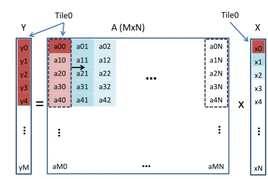
In this case, the optimum production-consumption (N intermediate results
are produced and directly consumed to compute the Y[0]) of array Y and
the sub-optimum data reuse of the array X have been found by splitting the
arrays into tiles (T ile0) according to the register file size (ineq. 5) (Fig. 1).
The register file inequality is:
(F P RF ≥(k0+p+ 1))&(Int RF ≥addr variables) (5)
where F P RF is the number of floating point registers, Int RF is the
number of integer registers, addr variables is the number of the addressing
variables (e.g.iterators),k0 is the size of Tile0 (k0= 5 in Fig. 1) andpis the
number of instructions that can be executed in parallel. In practicek0≥p.
k0,pand 1 registers are allocated for Y, A and X arrays, respectively. The
a00 a01 a02 a0N
a10 a11 a12 a1N
a20 a21 a22 a2N
a30 a31 a32 a3N
a40 a41 a42 a4N
aM0 aMN
y0
y1
y2
y3
y4
yM
=
x
Y A (MxN) X
Tile0 Tile0
…
…
…
…
…
…
x0
x1
x2
x3
x4
xN
…
Fig. 1 The proposed methodology when (k0+ 1)×N≺L1
once; thus, just one register is needed to store the A’s elements; however, ifp
instructions can be executed in parallel, pregisters are needed for matrix A
to have all function units working in parallel (p≥1).
The scheduling follows. The first k0 elements of the first column of A
(Fig. 1) make a tile (T ile0). All the tile’s elements are multiplied by the
first-top element of X (data reuse of X) and their results are stored into the first-first-top
k0elements of Y (T ile0). After the multiplication of all tile’s elements by X(0),
the tile is moved by one position to the right and all its elements are multi-plied by X(1), etc. The results are always stored in-place, namely in the same registers, exploiting production-consumption of intermediate results of Y.
Ac-cording to the above schedule the (Y, X, A) arrays are fetched (M, M2/k0, M)
instead of (M, M2, M) times (when the row-column schedule is used),
respec-tively.
Having only one level of a typical data cache, the time needed for the array elements to be loaded/stored, is approximated by eq. 6:
Tdata=max(
L1r×L1loads+L1s×L1stores
L1ports
,
M M r lineL1
×M Mloads+M M s×M Mstores×
⌈k0/lineL1⌉
k0 ) (6)
where L1r,L1s andM M r,M M s are the load/store latency values of L1
and main memory, respectively and lineL1 is the number of L1 data cache
line elements.L1portsis number of L1 read and write ports.L1loads,L1stores,
M MloadsandM Mstoresare the number of elements loaded/stored from/to L1
and main memory, respectively.M M rvalue is not a constant number since it
depends on the number of different main memory locations/pages are accessed.
[image:9.595.95.367.85.266.2]are written to main memory for eachk0elements. For data cache architectures where reads and writes are executed in parallel, eq. 6 is slightly different; we also assume that hardware prefetchers do not exist (which normally holds for embedded processors).
TheL1loads,L1stores,M Mloads andM Mstores values of eq. 6, depend on
the arrays size and on the data cache size. If the k0 rows of A and X remain
in L1 data cache, the number of L1 misses is low; on the other hand, if they are larger than the L1 data cache size, the number of the L1 misses increases, and therefore the number of L2/main memory accesses too.
In the case that the k0 rows of A and the X fit in L1 data cache ((k0+
1)×N×dtype≺L1), theTdatavalue of eq. 6 is given by:
Tdata=max(
L1r L1ports
×(M ×N+M ×N
k0 ) + L1s L1ports
×M,
M M r
lineL1×(M ×N+N) +M M s×
M× ⌈k0/lineL1⌉
k0 ) (7)
TheL1loads,L1stores,M MloadsandM Mstoresvalues of eq. 7, are obtained
from Table 1 (see 1 level of data cache and tiling for RF).
On the other hand, in the case that thek0rows of A and the X do not fit
in L1 data cache and for square matrix A of sizeM ×M, eq. 6 and Table 1
give:
Tdata=max(
L1r L1ports
×(M2/k1 +M2+M2/k0) + L1s
L1ports
×M2/k1,
M M r lineL1
×(M2/k1 +M2+M) +M M s×M2/k1×⌈k0/lineL1⌉
k0 ) (8)
To achieve the minimum Ttotal value (eq. 1), all (k0, k1) values achieving
small Tdata values (eq. 8) are selected (M M r ≻ L1r). Then these solutions
are tested and the fastest is picked. These solutions are tested since we cannot
approximate theTaddressing value.
In the case that the sum of thek0rows of A and the X array size is larger
than L1 data cache size, i.e. (k0+ 1)×N ≻ L1, the X array does not fit
in L1 data cache and thus it is not fetched once but N/k0 times from the
upper-slower memory of L1. To decrease the number of data accesses of the upper memory, loop tiling is applied by fully utilizing the L1 data cache size and associativity. Tiling is applied so the X array remains in L1 data cache
since it is reusedN/k0 times.
Regarding the efficient use of L1 data cache, A and X arrays are partitioned
into Tile1 tiles, of sizek0×k1 andk1 respectively; the largestk1size is picked,
for which the size of the data of one Tile1 of A (size ofk0×k1) and one Tile1
L1×(assocL1−k−1)
assocL1 ≤dtype×k0×k1≤
L1×(assocL1−k) assocL1 ,
k=⌈k1×dtype
L1/assocL1⌉ ≤
assocL1
2 (9)
wherek1 is the tile size in elements,dtypeis the size of the array elements
in bytes (e.g. for float numbers dtype= 4), L1 is the size of L1 data cache,
assocL1 is L1 data cache associativity,assocL1≻1 here (e.g for an 8-way set
associative cache,assocL1= 8).kis an integer and it gives the number of L1
data cache lines with identical L1 addresses used for one Tile1 of X; for the remainder of this paper we will more freely say that we use k cache ways for
X andassocL1−k cache ways for A (in other words, A and X are written in
separate data cache ways).
Let us explain Ineq. 9, in more detail. Ineq. 9 is introduced to minimize the number of L1 data cache misses and therefore the number of upper memory
accesses. Given that each row of A is multiplied by X, X is reusedM times,
and thus, it has to remain in L1 data cache. To do this, cache lines of A are
written in L1 without conflict with the X ones. This is achieved by loadingk0
sub-rows of A (Tile1 of A) and one sub-row of X (Tile1 of X), into separate L1 ways. This is achieved by storing the A array tile-wise in main memory
(consecutive main memory locations) and by using (k× L1
assocL1) L1 memory
size for X and ((assocL1−k)× assocL1L1) L1 memory size for A (ineq. 9).
We can more freely say that this is equivalent to using k cache ways for X
and (assocL1−k) cache ways for A. An empty cache line is always granted
(with respect to the size of the cache) for each different modulo of A and X memory addresses. It is important to say that if associativity is not taken into
account and L1 ≥ (k0×k1+k1) is used instead of ineq. 9, the number of
L1 misses will be much larger because A and X will conflict with each other. To our knowledge, this is the first time for an MVM algorithm that the cache associativity is utilized. Furthermore, the Y array is stored into main memory
infrequently (usually 1-2 cache lines are written to memory whenk0sub-rows
of A have been multiplied by X); thus the number of L1 conflicts due to Y can be neglected (if a victim cache exists, then these conflicts never occur).
In the case that the data cache is direct mapped (assocL1= 1), loop tiling
is not efficient since no tile can remain in data cache due to the cache modulo effect.
The scheduling of the Tile1 tiles follows (Fig. 2). All Tile1 of the first block column of A are multiplied by the first Tile1 of X. Then, all Tile1 of the second block column of A are multiplied by the second Tile1 of X; the procedure ends when all Tile1 of the last block column of A have been multiplied by the last Tile1 of X. Suppose an architecture with one level of data cache. Regarding
L1 data cache, the numbers of load/store instructions for the (Y, A, X)
ar-rays (A is a square matrix) are:L1loads=M ×(M/k1, M, M/k0), L1stores=
M ×(M/k1). Regarding main memory (MM), the numbers of load/store
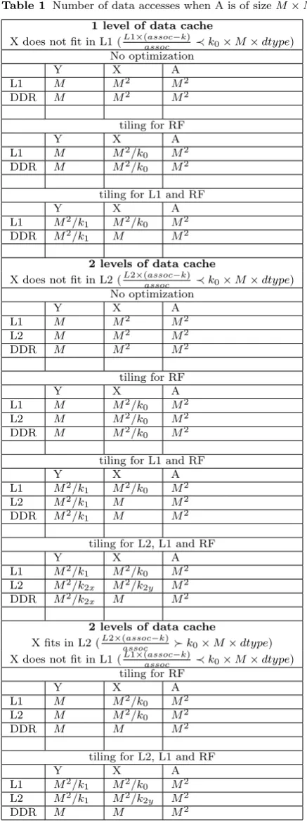
Table 1 Number of data accesses when A is of sizeM×M
1 level of data cache
X does not fit in L1 (L1×(assoc−k)
assoc ≺k0×M×dtype)
No optimization
Y X A
L1 M M2 M2
DDR M M2 M2
tiling for RF
Y X A
L1 M M2/k
0 M2
DDR M M2/k0 M2
tiling for L1 and RF
Y X A
L1 M2/k
1 M2/k0 M2
DDR M2/k
1 M M2
2 levels of data cache
X does not fit in L2 (L2×(assoc−k)
assoc ≺k0×M×dtype)
No optimization
Y X A
L1 M M2 M2
L2 M M2 M2
DDR M M2 M2
tiling for RF
Y X A
L1 M M2/k
0 M2
L2 M M2/k
0 M2
DDR M M2/k
0 M2
tiling for L1 and RF
Y X A
L1 M2/k
1 M2/k0 M2
L2 M2/k
1 M M2
DDR M2/k
1 M M2
tiling for L2, L1 and RF
Y X A
L1 M2/k
1 M2/k0 M2
L2 M2/k
2x M2/k2y M2
DDR M2/k
2x M M2
2 levels of data cache
X fits in L2 (L2×(assoc−k)
assoc ≻k0×M×dtype)
X does not fit in L1 (L1×(assoc−k)
assoc ≺k0×M×dtype)
tiling for RF
Y X A
L1 M M2/k
0 M2
L2 M M2/k
0 M2
DDR M M M2
tiling for L2, L1 and RF
Y X A
L1 M2/k
1 M2/k0 M2
L2 M2/k
1 M2/k2y M2
M ×(M/k1). If tiling for L1 data cache is not applied, the numbers of main
memory load/store instructions areM×(1, M, M/k0) andM respectively
(Ta-ble 1). Given thatk1≫k0, the number of main memory accesses is decreased.
The k0 value produced by ineq. 5, is the value minimizing the number of
load/store instructions and the number of register spills. Furthermore, thek1
value produced by ineq. 9, minimizes the number of L1 data cache misses (or
equivalent the number of main memory accesses here), given the k0 value.
However, these two sub-problems depend on each other and therefore by de-creasing the number of main memory data accesses, the number of L1 data accesses is increased. The number of the main memory data accesses is
mini-mized when thek1 value is maximized, according to ineq. 9; also the number
of the L1 data cache accesses is minimized when the k0 value is maximized
according to ineq. 5; however, according to ineq. 9, when k1 increases thek0
decreases (the maximum k1 value is given for k0 = 1). There is a trade-off
on the (k0, k1) selection and thus the minimum Tdata value depends on the
target architecture parameters. The proposed methodology optimizes these
two subproblems together as one problem and not separately; the (k0, k1)
val-ues are found theoretically according to the memory hierarchy architecture parameters, eq. 6.
Furthermore, the Tile1 of A are chosen to be as large as possible in the x-axis only. This is because i) the larger the tile of A, the larger the production and consumption of Y (as the Tile0 of A is moved by one position to the right in Fig. 1, the elements of Y are produced-consumed) ii) by tiling only x-dimension, a lower number of addressing instructions is achieved (there is one loop less), and iii) the larger the Tile1 of A is the larger the data reuse of X, as tiles are accessed in a column-wise way; this is because each Tile1 of X
is fetched just once. Although the results are stored into memoryN/k1times,
thek1 value is maximum, since Tile1 of A is as large as possible in the x-axis
dimension.
Regarding 2 level data cache architectures, if the following inequality holds
M ×k1+M +k1≻L2 (the Y array, all Tile1 tiles of one block column of A
and one Tile1 of X, do not fit in L2 data cache), theY array is loaded/stored
not once butM/k1times, from main memory. To decrease the number of main
memory data accesses, loop tiling is applied by fully utilizing the L2 data cache size and associativity. Tiling is applied so that the Y array remains in L2 data
cache, as it is loaded-reusedN/k1 times.
Regarding the efficient use of L2 data cache, the Y and A arrays are further
split into Tile2 tiles (Fig. 2); one Tile2 of Y (size ofk2y), one Tile2 of A (size
of k2y×kk2x) and one Tile2 of X size ofk2x, fit in L2 data cache, ineq. 10
(Fig. 2). The Tile2 tiles are multiplied by each other exactly as the Tile1 tiles.
L2×(assocL2−3) assocL2
≺dtype×k2y×k2x≤
L2×(assocL2−2) assocL2
(10)
Ineq. 10 satisfies that Tile2 of X and Tile2 of Y remain in L2 data cache;
=
x
…
…
…
…
…
N... ... ... ... ... Element
...
..
.
Y
A (MxN)
X
k1 k0
k0x k1 k1x 1
T
il
e
0
k2y
k1
…
Tile 2
…
k0
Tile1 Tile 2
Tile 1
…
…
…
…
…
…
…
…
…
k2y
k2x
Tile 2
Fig. 2 The proposed methodology with three levels of tiling (L2, L1, RF). The tiles that
are multiplied by each other are with the same color.
that the maximum L2 size needed for the Y, A and X arrays isL2/assocL2,
L2×(assocL2−2)
assocL2 andL2/assocL2, respectively.
Having these two tiles in L2, X is fetched just once while Y is fetched
M/k2x times, from main memory. The number of main memory accesses is
minimized when k2x = M, but in this case k2y value is decreased and the
number of L2 data cache accesses is increased (Table 1); there is trade off and
thus thek2x andk2y values are found theoretically according to the memory
hit latency values. For most general purpose processors where L2 data cache
size is large, k2x = M. In most cases, we select k2x ≫ k2y since the main
memory is many times slower than data cache.
The (k2y, k2x, k1, k0) values, are computed by optimizing the following
sub-problems, as one problem and not separately, as they depend on each other; these are the sub-problems of minimizing the number of L1, L2 and main memory accesses.
Having two levels of data cache, the time needed for the array elements to be fetched is:
Tdata=max(
L1r×L1loads+L1s×L1stores
L1ports
,
L2r lineL1
×L2loads+L2s×
L2stores× ⌈k0/lineL1⌉
[image:14.595.81.409.76.329.2]M M r lineL2
×M Mloads+M M s×
M Mstores× ⌈k0/lineL2⌉
k0 ) (11)
where L2r andL2s are the L2 cache read and write latencies. In the case
that modulo(k0, lineL2) 6= 0 the number of main memory stores is slightly
different as it depends on themodulo(k0, lineL2) value.
Eq. 11 and table 1 give:
Tdata=max(
L1r×(M2/k1+M2/k0+M2) +L1s×M2/k1 L1ports
,
L2r lineL1
×(M2/k2x+M2/k2y+M2) +L2s×
M2/k2
x× ⌈k0/lineL1⌉
k0 ,
M M r lineL2
×(M2/k2x+M+M2) +M M s×
M2/k2
x× ⌈k0/lineL2⌉
k0 ) (12)
Normally, M M r ≻ 40, 3 ≤ L2r ≤ 7 and L1r = 1. All (k0, k1, k2y, k2y)
values giving a smallTdatavalue according to the above inequalities are taken.
Then, these schedules are tested and the fastest is picked. Furthermore, solu-tions for zero, one and two levels of tiling are selected, as tiling increases the number of load/store and addressing instructions.
Regarding full memory hierarchy utilization, one level of tiling for each level of data cache and one more for the register file is used; loop tiling decreases the number of data cache misses but increases the number of load/store and addressing instructions (typically one more level of tiling in MVM algorithm adds two additional loops). However, tiling for each level of data cache is not performance efficient in several cases, as the additional number of instructions (both load/store and arithmetic) may degrade performance.
To summarize, the Tdata value for 1 level of tiling is given by eq. 7 and
eq. 8, while theTdata value or 2 levels of tiling is given by eq. 12. Also, eq. 9
and eq. 10, give the tile sizes.
3.1.2 Row-wise data array layout of A - CPUs without SIMD
Regarding register file utilization (if the k0 rows of A and X fit in L1 data
cache), the scheduling explained in the previous paragraph is used. However,
in the row-wise case, if the register file size is large and thusk0value is large,
the main memory bandwidth is increased, degrading performance; this is be-cause the elements of each sub-row of A are written in different main memory locations (and also in different main memory pages); reading from a large
number of different main memory locations needs more time. Therefore, k0
value has an upper threshold which is bounded by main memory parameters (this is further explained into subsection 3.2).
Regarding L1 data cache, ineq. 9 does not hold in the row-wise case. If
the data array layout of A is row-wise, the elements of the k0 sub-rows of
values, they haveN×4 bytes distance. This means that by using ineq. 9, the Tile1 of X does remain in L1 data cache, as the cache lines of A will conflict with the cache lines of X. To overcome this problem, the following inequality is introduced.
k0≤assocL1−1 (13)
According to ineq. 13, one L1 way is used for each sub-row of A and another
one for the Tile1 of X (assoc≻1). Normally, thek0value of the row-wise case,
is smaller than the k0 value of the tile-wise case and, thus, a larger number
of data accesses is achieved in this case. When ineq. 13 holds, tiling is applied
according to ineq. 14; the maximumk1value is selected so that Tile1 of X fit
in one L1 cache way.
dtype×k1≤ L1
assocL1
(14)
All the (k0, k1) values giving a small number ofTdataaccording to the above
inequalities are taken. To our knowledge, this is the first time that loop tiling is applied by analyzing i) the data cache size, ii) the data cache associativity and iii) data arrays layout in main memory as one problem and not separately. Regarding L2 data cache, tiling is applied as explained in the previous
paragraph, but k2x = N. In this case, all the sub-rows of each Tile2 of A
are written in non consecutive main memory locations and, thus, in non con-secutive data cache locations; therefore, the number of L2 data cache misses
is increased. To minimize the number of L2 data cache misses, k2x = N; in
this case, all the sub-rows of Tile2 of A are of size N and they are written in
consecutive main memory locations.
3.1.3 CPUs with SIMD
Most of the today’s general purpose processors have SIMD (Single Instruction Multiple Data) unit in order to further increase performance by using vector operations. However, to efficiently use the SIMD unit, i) the schedule deci-sion must take into account the instruction selection problem, since there are
instructions with variant latency/throughput values (e.g.’hadd’ instructions
have very large latency and throughput values), and ii) the data have to be aligned in main memory according to the SIMD registers size.
Regarding SIMD architectures, the schedule explained in subsection 3.1.1 and 3.1.2, is not performance efficient. To implement the above schedule into AVX/SSE technology, several copies of each element of X have to be stored into 1 YMM/XMM register depending on the elements’ size and registers’ size; loading just one element needs more time than loading a whole L1 cache line and this is why this schedule is not performance efficient. SIMD unit introduces additional constraints which are fully exploited here.
while SSE technology supports 128-bit registers. The optimum production-consumption of array Y and the sub-optimum data reuse of array X have been selected by splitting the arrays into tiles according to the number of XMM/YMM registers (eq. 15).
Regs=k0 + 1 + 1 (15)
where Regs is the number of the XMM/YMM registers and k0 is the
number of the registers used for Y array. Thus, (Regs−2) registers for Y, 1
register for A and 1 register for X, are used.
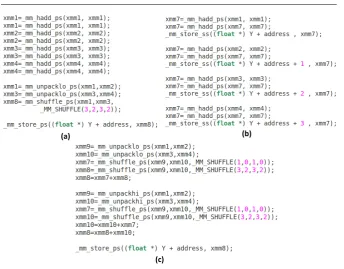
The scheduling follows. Consider that there are 8 XMM registers (XMM0 : XMM7) of size 128-bit and the arrays contain floating point data (4 bytes each). The first 4 elements of A and X are fetched into XMM0 and XMM1, respectively. They are multiplied by each other and the result is stored into XMM2. Then, the first 4 elements of the second row of A are loaded into XMM0 again; XMM0 is multiplied by XMM1 and the results is stored into XMM3. The procedure is repeated for the 3rd, 4th, 5th and 6th row of A (XMM2:XMM7 contain the values of Y[0]:Y[5] respectively). Afterwards, the second quartet of X is loaded into XMM1 and the second quartet of the first row of A is loaded into XMM0; they are multiplied by each other and the result is accumulated into XMM2. Then the second quartet of the second row of A is loaded into XMM0 again, etc. When the first 6 rows of A have been fully multiplied by X, the four values of each one of XMM2:XMM7 registers
are summed and the results are stored into main memory (Y array),e.g.the
sum of the four XMM2 values is Y(0). The above procedure continues until all rows of A have been multiplied by X. The Y array is written in memory
once, while array X is loadedN/(Regs−2) times.
There are several ways to sum theXM M2 :XM M7 data, i) to accumulate
the values of each XMM register, to pack the results into new ones and to store four values in main memory at once (Fig. 3-a), ii) to accumulate the values of each XMM register and store each single Y value separately (Fig. 3-b), iii) to unpack the XMM values of the registers and to pack them into new ones in order to add elements of different registers (Fig. 3-c). Within most architectures, the third one is faster than the other two, because unpacking and shuffle operations have smaller latency and throughput values than hadd operations. Also, the second is faster than the first within most architectures, because the store and add operations can be executed in parallel.
Regarding L1 data cache utilization, the schedule used is the same as in the previous subsections. However, loop-tiling is less effective here, because most of the todays general purpose processors have hardware prefetchers, for both L1 and L2 caches, decreasing the number of data cache misses.
By using SIMD, eq. 2 changes into eq. 16 as tiling further increases the
number of SSE instructions; as the k1 value decreases, the number of SSE
(a) (b)
(c)
Fig. 3 Three different ways for unpacking the multiplication results; XMM1, XMM2,
XMM3, XMM4 contain the Y values. For most SIMD architectures, the three schedules are in increased performance order.
Tdata=max(Tdata, Tmatrix−operations+c×
M
k1, Taddressing) (16)
where cis the sum of the SSE instruction latencies shown in Fig. 3.
3.2 Multi-core CPUs
Having more than one core, the MVM problem is partitioned into smaller MVM sub-problems. Each sub-problem corresponds to a thread and each thread is executed in one core only. Each thread must contain at least a spe-cific number of instructions, to minimize the core ’idle-time’; this is because partitioning MVM into smaller sub-problems results in thread initialization and synchronization time comparable to the thread execution time, leading to low performance. This is an additional constraint.
Most of today’s multi core processors typically contain 2 or 3 levels of cache, having either i) separate L1 data and instruction caches and a shared L2 cache or ii) separate L1 data and instruction caches, separate unified L2 caches and a shared L3 cache, respectively. All caches have an LRU replacement policy.
[image:18.595.71.416.76.345.2]This is achieved by partitioning the matrix A horizontally intoq equal parts
and by partitioning the array Y into qequal parts, whereq is the number of
the cores. The multiplication of each part of A by X makes a different thread.
The MVM problem is partitioned into q different threads and each thread
writes on its own part of Y into main memory. Each thread is executed at only one core and the schedule is almost the same as in Subsection 3.1 (the differences are explained below).
By partitioning the MVM into threads and running them in parallel, the performance critical parameters are main memory latency and bandwidth val-ues. Although, data reuse and data cache hierarchy have been fully utilized, minimizing the number of X and Y main memory accesses, the elements of A (which are much more than X and Y), are used only once (no data reuse);
thus, the number of main memory accesses of A cannot be reduced (N ×M
loads); for one matrix-vector multiplication to be executed, a different value of A is needed and this is why main memory latency cannot be hidden by the cache (CPU remains idle several cycles).
Thus, the MVM execution time depends on the time needed for matrix A to be loaded from main memory. This is why a large core utilization factor cannot be achieved. MVM performance is restricted by main memory latency and bandwidth values, so there is no way to increase performance more than this.
Furthermore, the main memory bandwidth would be low if we adopt the schedule explained in Subsection 3.1. This is because each thread accesses data from many different main memory locations. To be more precise, the el-ements of each sub-row of A are written in different main memory locations, so reading from different main memory locations needs more time.
There-fore, as the k0 value decreases, the time needed fetching the elements of A
decreases. On the other hand, as the k0 value increases according to eq. 15,
the number of load/store instructions and the number of data cache accesses decreases (however, it is not the critical parameter here). Therefore, the
pro-posed methodology gives a differentk0value according to the number of cores
used and main memory parameters; as the number of the cores used increases,
thek0value decreases.
In the case that the data array layout is tile-wise, MVM performance is highly increased. This is because i) array A is accessed from consecutive main memory locations only, increasing the main memory bandwidth, ii) the hard-ware prefetchers can prefetch the data of A because only one page is accessed, iii) the X array fits in the private caches in most cases.
In the case that the cache hierarchy consists of 3 levels of cache and thus a private L2 cache for each core exists, the X array can fit in all the L2 memories even if no tiling for data cache is applied; in this way performance is increased even more. In the case that the data array layout of A is tile-wise, X always fits in L2 cache as L2 size in modern architectures is large enough. On the other hand, if the array layout of A is row-wise, ineq. 17 must hold for the array X to remain in L2.
L2private×(assoc−k0)
assoc ≥N×dtype (17)
where L2private is the size of the L2 private cache.
According to ineq. 17, one L2 cache way is needed for each row of A. This
is because the elements of the k0 different rows of A are not in consecutive
main memory locations and, thus, they are not fetched in consecutive L2 cache locations.
Regarding 3 level data cache architectures, tiling for data cache can be
applied in several ways, i.e. tiling for i) L1, ii) L2 and iii) both. However,
by applying tiling for the cache, the number of main memory accesses is not further decreased, as both Y and X remain in L3 even if no tiling is applied because L3 shared cache size is very large in modern architectures; in general, performance is slightly affected by applying tiling for general purpose proces-sors. This is because the critical parameter is the number of main memory accesses.
4 Experimental Results
The experimental results for the proposed methodology, presented in this sec-tion, were carried out with a Pentium Intel core 2 duo E6550 [1], a Pentium Intel Core 2 Duo T6600 at 2.20GHz [2] and with a Pentium Intel i7-3930K (6 cores) at 3.2Ghz [3], all using SSE/AVX instructions and ATLAS 3.8.4, respectively. Also, the Valgrind [36] tool and SimpleScalar simulator [42] are used to measure the total number of L1 and L2 data cache accesses and misses. The first processor contains 8 128-bit XMM registers, L1 data and instruction caches of size 32 kbytes and shared L2 cache of size 4 Mbytes. The second processor contains 16 XMM registers, L1 data and instruction caches of size 32 kbytes and shared L2 cache of size 3 Mbytes. The third processor contains 16 256-bit YMM registers, L1 data and instruction caches of size 32 kbytes, L2 unified cache of size 256 kbytes and shared L3 cache of size 12 Mbytes. All processors use the Operating system Ubuntu and the gcc-4.4.3 compiler. Fur-thermore, SimpleScalar simulator [42] is used to measure the number of data cache misses when no SIMD is used. In the experimental procedure, square
matrix sizes (N×N), including floating point numbers (4 bytes) as elements,
1.23 1.26
1.22 1.24 1.24
1.20 1.21
1.24 1.23 1.27
1.00 1.00 0.99 0.99 0.99 0.99 0.99 1.00 0.99 0.99 1.00 1.00 1.00 1.00 1.01 1.01 1.01 1.01 1.01 1.01 0.90 1.00 1.10 1.20 1.30 1.40 1.50
240 600 960 1200 1920 2880 3840 4800 5760 7680
R a ti o s o f th e c o rr e sp o n d in g p a ra m e te rs
Input size N
Comparison of the proposed methodology versus ATLAS using 1 core
speedup - arch1 L1 accesses - L/S - arch1 L2 accesses - arch1 DDR accesses - arch1 speedup - arch2 speedup_tile-wise - arch2
Fig. 4 Comparison of the proposed methodology over ATLAS on Pentium E6550 (arch1)
and T6600 (arch2). The executables run in one core of the 2 that exist.
it will toggle the thread among the cores, degrading performance because of the data movement involved.
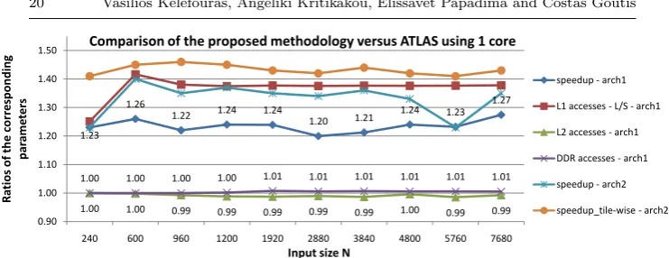
First, a performance comparison is made for Intel E6550 (arch1) and Intel T6600 (arch2), by using only the one core of the 2 that exist(Fig. 4). The
proposed methodology is compared with thecblas sgemv routine of ATLAS
and the average execution time among many executions is shown. Tiling for L1 and L2 cache is not performance efficient for Intel E6550 and Intel T6600. Regarding L2, tiling is not efficient because the whole Y and X arrays and several rows of A are of smaller size. Regarding L1, tiling is memory efficient but it is not performance efficient. Tiling is used in order to decrease the num-ber of cache misses; however, the extra load/store and addressing instructions inserted here overlap the data locality advantage. Regarding register file uti-lization, both processors contain 8 XXM registers and thus loop tiling with
k0= 6 is applied (ineq. 15).
The proposed methodology is on average 1.23 and 1.33 faster than
AT-LAS library on E6550 (arch1) and T6600 (arch2), respectively; this is because it achieves a lower number of load/store instructions or equivalently L1 data
cache accesses. For arch1, we achieve 1.38 times less load/store instructions
than ATLAS. The number of load/store instructions is much less since the register file size is fully utilized (ineq. 15); first, we use all the available XMM registers and second we use them efficiently according to the data reuse. Re-garding the number of main memory data accesses, the proposed methodology achieves approximately the same number with ATLAS (we achieve about 1% less main memory data accesses); the gain is small because L2 caches are large and the whole Y and X arrays and several rows of A can fit in L2. As it was explained in the previous Subsections, the three arrays are accessed only once from main memory (table 1) and thus the number of main memory data accesses is the minimum. Although we achieve only 1% less main memory accesses, this gain is significant since only the number of Y and X data ac-cesses can be decreased and not of A (matrix A is many times larger than Y
[image:21.595.56.427.70.213.2]1.80E+05 1.85E+05 1.90E+05 1.95E+05 2.00E+05 2.05E+05 2.10E+05 2.15E+05 2.20E+05 2.25E+05
10 15 20 25 30 40 50 100 200 600
N
u
m
b
e
r
o
f
L1
d
a
ta
c
a
ch
e
r
e
p
la
ce
m
e
n
ts
Tile size in elements
Number of L1 data cache replacements versus tile size
Fig. 5 Number of L1 data cache replacements for different tile sizes.
only once (no data reuse). Regarding the number of L2 cache accesses, the proposed methodology achieves approximately the same number with ATLAS (we achieve about 1% more L2 data accesses). This is because ATLAS ap-plies loop tiling for L1 here; it is important to say that we do not provide the schedule achieving the lower number of data cache accesses here, but the schedule achieving the best performance. Furthermore, the proposed method-ology execution time increases proportionally to the matrix size, while ATLAS execution time does not; this is because ATLAS applies different schedules.
In the case that the data array layout of A is tile-wise, the speedup is
fur-ther increased (about 1.42%) for two reasons. First, the A elements are fetched
from consecutive main memory locations (if the data array layout is row-wise, the elements of each sub-row of A are written from different main memory lo-cations and reading from different memory addresses needs more time); in this way the main memory bandwidth is increased. Second, the hardware prefetch-ers can prefetch the data of A.
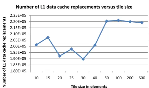
An evaluation for different tile sizes for L1 data cache is also performed on SimpleScalar simulator (Fig. 5). An architecture with one level of data
cache of size 1 kbyte and 8-way associative, is used. Also,N= 600. According
to ineq. 14, the best tile size here is T = 30. This is verified by Fig. 5 too.
As the tiles fit in L1 data cache, the number of cache replacements is low (T ile≺30), but when the tiles become larger than the L1 size, the number of
L1 replacements becomes high (T ile≻30).
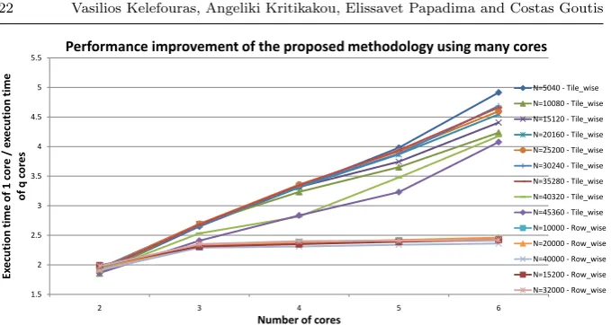
An evaluation for many cores of one CPU is also performed on i7-3930K (6 cores) (Fig. 6). To our knowledge, no related work exists for dense MVM on multi-core processors. Furthermore, the ATLAS library does not provide routines for more than one core. Thus, the speedups shown in Fig. 6 and Fig. 7 are over the proposed methodology for one core. By using only two
cores, the speedup is (near)-optimum (from 1.88 up to 1.99, depending on the
[image:22.595.120.361.82.224.2]Performance improvement of the proposed methodology using many cores 1.5 2 2.5 3 3.5 4 4.5 5 5.5
2 3 4 5 6
E xe cu ti o n t im e o f 1 c o re / e xe cu ti o n t im e o f q c o re s
Number of cores
N=5040 - Tile_wise N=10080 - Tile_wise N=15120 - Tile_wise N=20160 - Tile_wise N=25200 - Tile_wise N=30240 - Tile_wise N=35280 - Tile_wise N=40320 - Tile_wise N=45360 - Tile_wise N=10000 - Row_wise N=20000 - Row_wise N=40000 - Row_wise N=15200 - Row_wise N=32000 - Row_wise
Fig. 6 Speedup of the proposed methodology for different number of cores
memory latency and bandwidth values. Regarding row-wise data array layout of matrix A, performance is not increased by providing more than 4 cores since the main memory cannot provide the operands in lower time. The speedup is
up to 2.45 (as the number of the cores increases, the proposed methodology
gives a lower k0 value as it has been explained in the proposed methodology
subsection). Regarding tile-wise data array layout of matrix A, MVM performs much better (the time needed to change the data array layout of A is not included) as the performance gain increases proportionally to the number of cores. This is because, i) all main memory accesses of A are performed at one memory page, ii) the hardware prefetchers can prefetch the data of A as only one page is accessed, and iii) the X array fits into the private caches in most
cases. However, speedup cannot exceed 4.92 value. Regarding the two largest
matrix sizes,i.e.N = 45360 andN = 40320, they achieve a slightly decreased
performance, as the X array cannot remain in private L2 cache.
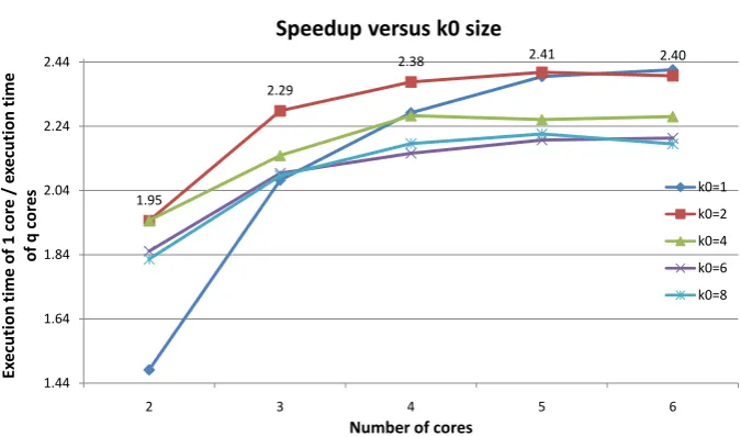
An evaluation for many differentk0 values is also performed on i7-3930K,
for the row-wise case (Fig. 7). Intel i7-3930K contains 16 256-bit AVX registers;
by using only one core (q= 1), only k0≥8 values achieve high performance
here. By using more than one cores, the main memory bandwidth increases as
thek0 value decreases; this is because the elements of each sub-row of A are
written in different main memory locations; reading from different addresses
needs more time. On the other hand, as the k0 value increases according to
eq. 15, the number of load/store instructions and the number of data cache accesses decreases. However, main memory is by far the most critical parameter
here and, thus, a small k0 value is selected according to the main memory
parameters. In the case that there are 5 or 6 cores, the main memory load is
very high, and thus k0 = 1 and k0 = 2 are the best values; in this case, the
register file and data cache utilization do not increase performance, as main
memory is the critical parameter. For the same reason,k0 = 1 value achieves
[image:23.595.73.413.67.248.2]Speedup versus k0 size
1.95
2.29
2.38 2.41 2.40
1.44 1.64 1.84 2.04 2.24 2.44
2 3 4 5 6
E xe cu ti o n t im e o f 1 c o re / e xe cu ti o n t im e o f q c o re s
Number of cores
k0=1 k0=2 k0=4 k0=6 k0=8
Fig. 7 Speedup of the proposed methodology for differentk0 values,N= 20160
5 Conclusions
In this paper, a new methodology for computing the Dense Matrix Vector Multiplication for both embedded (single core processors without SIMD unit) and general purpose processors (single and multi-core processors, with SIMD unit) is presented. This methodology achieves higher execution speed than the ATLAS state of the art library and the final schedule is found theoreti-cally according to the memory hierarchy parameters. Furthermore, by utilizing software and hardware parameters, the number of solutions tested is orders of magnitude smaller; therefore, instead of searching the whole space, only a small number of solutions is tested.
References
1. Intel core 2 duo processor E6550 http://ark.intel.com/Product.aspx?id=30783. URL http://ark.intel.com/Product.aspx?id=30783
2. Intel core 2 duo processor T6600 http://ark.intel.com/products/37255/Intel-Core2-Duo-Processor-T6600. URL http://ark.intel.com/products/37255/Intel-Core2-Duo-Processor-T6600
3. Intel i7-2600K Processor http://ark.intel.com/products/52214. URL http://ark.intel.com/products/52214
4. Parallel methods for matrix-vector multiplication. URL http://www.hpcc.unn.ru/mskurs/ENG/DOC/pp07.pdf
5. OpenBlas (2012). URL http://xianyi.github.com/OpenBLAS
[image:24.595.73.411.81.280.2]7. Arabnia, H.: A distributed stereocorrelation algorithm. In: Computer Communications and Networks, 1995. Proceedings., Fourth International Conference on, pp. 479–482. IEEE (1995)
8. Arabnia, H.R.: A parallel algorithm for the arbitrary rotation of digitized images using process-and-data-decomposition approach. Journal of Parallel and Distributed Com-puting10(2), 188–192 (1990)
9. Arabnia, H.R., Bhandarkar, S.M.: Parallel stereocorrelation on a reconfigurable multi-ring network. The Journal of supercomputing10(3), 243–269 (1996)
10. Arabnia, H.R., Oliver, M.A.: A transputer network for the arbitrary rotation of digitised images. The Computer Journal30(5), 425–432 (1987)
11. Arabnia, H.R., Oliver, M.A.: Arbitrary rotation of raster images with SIMD machine architectures. Computer Graphics Forum6(1), 3–11 (1987)
12. Arabnia, H.R., Oliver, M.A.: A transputer network for fast operations on digitised images. Computer graphics forum8(1), 3–11 (1989)
13. Arabnia, H.R., Smith, J.W.: A reconfigurable interconnection network for imaging op-erations and its implementation using a multi-stage switching box. pp. 349–357 (1993) 14. Bacon, D.F., Graham, S.L., Oliver, Sharp, J.: Compiler Transformations for
High-Performance Computing. ACM Computing Surveys26, 345–420 (1994)
15. Baker, A.H., Schulz, M., Yang, U.M.: On the performance of an algebraic multigrid solver on multicore clusters. In: Proceedings of the 9th interna-tional conference on High performance computing for computainterna-tional science, VECPAR’10, pp. 102–115. Springer-Verlag, Berlin, Heidelberg (2011). URL http://dl.acm.org/citation.cfm?id=1964238.1964252
16. Bhandarkar, S.M., Arabnia, H.R.: The Hough transform on a reconfigurable multi-ring network. Journal of Parallel and Distributed Computing24(1), 107–114 (1995) 17. Bhandarkar, S.M., Arabnia, H.R.: The REFINE Multiprocessor - Theoretical Properties
and Algorithms. Parallel Computing21(11), 1783–1805 (1995)
18. Bhandarkar, S.M., Arabnia, H.R., Smith, J.W.: A reconfigurable architecture for im-age processing and computer vision. International journal of pattern recognition and artificial intelligence9(02), 201–229 (1995)
19. Bilmes, J., Asanovi´c, K., Chin, C., Demmel, J.: Optimizing Matrix Multiply using PHiPAC: a Portable, High-Performance, ANSI C Coding Methodology. In: Proceedings of the International Conference on Supercomputing. ACM SIGARC, Vienna, Austria (1997)
20. Cooper, K.D., Subramanian, D., Torczon, L.: Adaptive Optimizing Compilers for the 21st Century. Journal of Supercomputing23, 2002 (2001)
21. Frigo, M., Johnson, S.G.: The Fastest Fourier Transform in the West. Tech. rep., Cam-bridge, MA, USA (1997)
22. Fujimoto, N.: Dense Matrix-Vector Multiplication on the CUDA Architecture. Parallel Processing Letters18(4), 511–530 (2008)
23. Fujimoto, N.: Faster matrix-vector multiplication on GeForce 8800GTX. In: IPDPS, pp. 1–8. IEEE (2008). URL http://dblp.uni-trier.de/db/conf/ipps/ipdps2008.html 24. Goumas, G., Kourtis, K., Anastopoulos, N., Karakasis, V., Koziris, N.:
Perfor-mance evaluation of the sparse matrix-vector multiplication on modern architec-tures. J. Supercomput.50(1), 36–77 (2009). DOI 10.1007/s11227-008-0251-8. URL http://dx.doi.org/10.1007/s11227-008-0251-8
25. Granston, E., Holler, A.: Automatic Recommendation of Compiler Options. In: In Proceedings of the Workshop on Feedback-Directed and Dynamic Optimization (FDDO (2001)
26. Guennebaud, G., Jacob, B., et al.: Eigen v3. http://eigen.tuxfamily.org (2010) 27. Hendrickson, B., Leland, R., Plimpton, S.: An Efficient Parallel Algorithm for
Matrix-Vector Multiplication. International Journal of High Speed Computing7, 73–88 (1995) 28. Intel: Intel MKL, available at http://software.intel.com/en-us/intel-mkl (2012) 29. Kisuki, T., Knijnenburg, P.M.W., O’Boyle, M.F.P., Bodin, F., Wijshoff, H.A.G.: A
31. Kulkarni, P., Hines, S., Hiser, J., Whalley, D., Davidson, J., Jones, D.: Fast searches for effective optimization phase sequences. SIGPLAN Not.39(6), 171–182 (2004). DOI 10.1145/996893.996863. URL http://doi.acm.org/10.1145/996893.996863
32. Kulkarni, P.A., Whalley, D.B., Tyson, G.S., Davidson, J.W.: Practical exhaustive opti-mization phase order exploration and evaluation. TACO6(1) (2009)
33. Michailidis, P.D., Margaritis, K.G.: Performance Models for Matrix Computations on Multicore Processors Using OpenMP. In: Proceedings of the 2010 International Con-ference on Parallel and Distributed Computing, Applications and Technologies, PD-CAT ’10, pp. 375–380. IEEE Computer Society, Washington, DC, USA (2010). DOI 10.1109/PDCAT.2010.52. URL http://dx.doi.org/10.1109/PDCAT.2010.52
34. Milder, P.A., Franchetti, F., Hoe, J.C., P¨uschel, M.: Computer Generation of Hard-ware for Linear Digital Signal Processing Transforms. ACM Transactions on Design Automation of Electronic Systems17(2) (2012)
35. Monsifrot, A., Bodin, F., Quiniou, R.: A Machine Learning Approach to Auto-matic Production of Compiler Heuristics. In: Proceedings of the 10th Interna-tional Conference on Artificial Intelligence: Methodology, Systems, and Applica-tions, AIMSA ’02, pp. 41–50. Springer-Verlag, London, UK, UK (2002). URL http://dl.acm.org/citation.cfm?id=646053.677574
36. Nethercote, N., Seward, J.: Valgrind: a framework for heavyweight dynamic binary instrumentation. SIGPLAN Not.42(6), 89–100 (2007). DOI 10.1145/1273442.1250746. URL http://doi.acm.org/10.1145/1273442.1250746
37. Park, E., Kulkarni, S., Cavazos, J.: An evaluation of different modeling techniques for iterative compilation. In: Proceedings of the 14th international conference on Compilers, architectures and synthesis for embedded systems, CASES ’11, pp. 65– 74. ACM, New York, NY, USA (2011). DOI 10.1145/2038698.2038711. URL http://doi.acm.org/10.1145/2038698.2038711
38. Pinter, S.S.: Register Allocation with Instruction Scheduling: A New Approach (1996) 39. Schmollinger, M., Kaufmann, M.: Algorithms for SMP-Clusters Dense Matrix-Vector Multiplication. In: Proceedings of the 16th International Parallel and Distributed Pro-cessing Symposium, IPDPS ’02, pp. 57–. IEEE Computer Society, Washington, DC, USA (2002). URL http://dl.acm.org/citation.cfm?id=645610.661893
40. See homepage for details: ATLAS homepage (2012). Http://math-atlas.sourceforge.net/ 41. Shobaki, G., Shawabkeh, M., Rmaileh, N.E.A.: Preallocation instruction scheduling with register pressure minimization using a combinatorial optimization approach. ACM Trans. Archit. Code Optim. 10(3), 14:1–14:31 (2008). DOI 10.1145/2512432. URL http://doi.acm.org/10.1145/2512432
42. Simplescalar, C.I., Burger, D., Austin, T.M.: The SimpleScalar Tool Set, Version 2.0. Tech. rep. (1997)
43. Sørensen, H.H.B.: High-Performance matrix-vector multiplication on the GPU. In: Pro-ceedings of the 2011 international conference on Parallel Processing, Euro-Par’11, pp. 377–386. Springer-Verlag, Berlin, Heidelberg (2012)
44. Stephenson, M., Amarasinghe, S., Martin, M., O’Reilly, U.M.: Meta optimization: im-proving compiler heuristics with machine learning. SIGPLAN Not.38(5), 77–90 (2003). DOI 10.1145/780822.781141. URL http://doi.acm.org/10.1145/780822.781141 45. Tartara, M., Crespi Reghizzi, S.: Continuous learning of compiler heuristics. ACM
Trans. Archit. Code Optim. 9(4), 46:1–46:25 (2013). DOI 10.1145/2400682.2400705. URL http://doi.acm.org/10.1145/2400682.2400705
46. Triantafyllis, S., Vachharajani, M., Vachharajani, N., August, D.I.: Compiler optimization-space exploration. In: Proceedings of the international symposium on Code generation and optimization: feedback-directed and runtime optimization, CGO ’03, pp. 204–215. IEEE Computer Society, Washington, DC, USA (2003). URL http://dl.acm.org/citation.cfm?id=776261.776284
47. Waghmare, V.N., Kendre, S.V., Chordiya, S.G.: Article: Performance Analysis of Matrix-Vector Multiplication in Hybrid (MPI + OpenMP). International Journal of Computer Applications22(5), 22–25 (2011). Published by Foundation of Computer Science
49. Whaley, R.C., Dongarra, J.: Automatically Tuned Linear Algebra Software. Tech. Rep. UT-CS-97-366, University of Tennessee (1997)
50. Whaley, R.C., Dongarra, J.: Automatically Tuned Linear Algebra Software. In: Super-Computing 1998: High Performance Networking and Super-Computing (1998)
51. Whaley, R.C., Dongarra, J.: Automatically Tuned Linear Algebra Software. In: Ninth SIAM Conference on Parallel Processing for Scientific Computing (1999). CD-ROM Proceedings
52. Whaley, R.C., Petitet, A.: Minimizing development and maintenance costs in supporting persistently optimized BLAS. Software: Practice and Experience35(2), 101–121 (2005) 53. Whaley, R.C., Petitet, A., Dongarra, J.J.: Automated Empirical Optimization of
Soft-ware and the ATLAS Project. Parallel Computing27(1–2), 3–35 (2001)
54. Williams, S., Oliker, L., Vuduc, R., Shalf, J., Yelick, K., Demmel, J.: Optimization of sparse matrix-vector multiplication on emerging multicore platforms. In: Pro-ceedings of the 2007 ACM/IEEE conference on Supercomputing, SC ’07, pp. 38:1– 38:12. ACM, New York, NY, USA (2007). DOI 10.1145/1362622.1362674. URL http://doi.acm.org/10.1145/1362622.1362674
55. Zhang, N.: A Novel Parallel Scan for Multicore Processors and Its Application in Sparse Matrix-Vector Multiplication. IEEE Transactions on Parallel and Distributed Systems