band gap of KNbO3-based ceramics
PASCUAL-GONZALEZ, Cristina
Available from Sheffield Hallam University Research Archive (SHURA) at:
http://shura.shu.ac.uk/18746/
This document is the author deposited version. You are advised to consult the publisher's version if you wish to cite from it.
Published version
PASCUAL-GONZALEZ, Cristina (2017). Processing-composition-structure effects on the optical band gap of KNbO3-based ceramics. Doctoral, Sheffield Hallam
University.
Copyright and re-use policy
optical band gap of KNbO3-based ceramics
Cristina Pascual-González
A thesis submitted in partial fulfilment of the requirements of
Sheffield Hallam University for the degree of Doctor of Philosophy
First of all, I would like to acknowledge the financial support of the Vice-Chancellor scholarship from Sheffield Hallam University, my main supervisor, Dr Antonio Feteira, for his support and guidance throughout my studies and my second supervisor, Dr Iasmi Sterianou, for her willingness to answer my ‘silly questions’.
I would also like to thank TO-BE cost action, which made possible my attendance to a summer school, different meetings and short term scientific mission in Universitat de Barcelona. Thank you to Dr. Ignasi Fina and Prof. Manuel Varela for their warm hospitality and sharing their knowledges about PLD with me.
I would also like to thank Dr Giorgio Schileo for his support since my first day in Sheffield and the band-gap measurements, and Carolina Elicker for her kindness and photovoltaic measurements.
At Sheffield Hallam University, I would like to thank Deeba Zahoor, Dr. Anthony Bell, Stuart Creasey and Paul Alender for their help with the instrumentation and the facilities in the laboratory and of course my colleagues of the Ceramic and Glass group, for their support every day and lovely company, specially Alex Scrimshire and Benjamin Allsopp, for their ‘english lessons’ and Georgia Christopoulou, for all the shared laughter and tears (but mostly, laughter) at the university. At Sheffield University, I would like to thank to Amir Kreshor, Shunshuke Murakani and Dawei Wang for the dielectric measurement and Raman Spectroscopy with temperature. At Instituto de Ciencia de Materiales de Madrid, I would like to express my gratitude to Miguel Algueró and Harvey Amorín for their encouragement and help to find a PhD position.
The PhD experience has been a crucial experience in my life and I would like to thank all who have helped me during this long journey.
Pero sobre todo quiero agradecer a Rebe todo su apoyo, cariño y compañía cada día, que ha sido fundamental durante mi estancia aquí.
Gracias a mi pequeña pero gran familia, sobre todo a mis padres por su apoyo y amor incondicional, a los que les debo todo lo que tengo.
I declare this thesis has been composed by myself, except collaborations that has been specified in the text, that were carried out at the University of Sheffield (Sheffield, United Kingdom), Universidade Federal de Pelotas (Pelotas, Brazil) and in the company Greatsolarcell (Manchester, United Kingdom). The work reported here has not been submitted for any other degree or professional qualification.
Some parts of the work reported in this thesis have been published or submitted for publication, as listed below. It is anticipated that further parts of this work will be submitted for publication in due course. The rest of papers published during the last three years are listed in APPENDIX H (section H.1.1).
1. C. Pascual-Gonzalez, G. Schileo, S. Murakami, A. Khesro, D. Wang, I. M. Reaney and A. Feteira. Continuously controllable optical band gap in orthorhombic ferroelectric
KNbO3-BiFeO3 ceramics. Applied Physics Letters, 110, 179202 (2017).
2. C. Pascual-González, G. Schileo, A. Kherso, I. Sterianou, D. Wang, I. M. Reaney and A. Feteira. Band gap evolution and piezoelectric-to-electrostrictive crossover in (1-x)KNbO3 - x(Ba0.5Bi0.5)(Nb0.5Zn0.5)O3 ceramics. Journal of Materials Chemistry C, 5 (8).
This present work is focused on band-gap engineering of solid-solutions based on KNbO3, which was proposed as a promising photoferroelectric (Grinberg et al., 2013). The strategy to narrow the band-gap of the parent KNbO3 (3.22 eV), relies on replacing Nb5+ by lower valence transition metals (Me3+)and K+1 by cations which maintain the compositions stoichiometric.
Ceramic processing of KNbO3 by conventional route was optimised in order to minimise K losses, which leads to the formation of a hygroscopic secondary phase, K4Nb6O17. This phase impairs the structural integrity of the samples. In addition, single-phase KNbO3 ceramics have the tendency to absorb moisture from the environment, increasing its conductivity near room temperature. Subsequently, all solid-solutions presented in this work, (1-x) KNbO3-x Ba0.5Bi0.5Nb0.5Zn0.5O3 and (1-x) KNbO3-x BiMeO3 (Me= Mn, Co and Ni) systems in a compositional range of 0≤x≤0.25, 0.90 KNbO3-0.1 BaNb0.5Ni0.5O3 and 0.98 K0.5Na0.5NbO3-0.02 BaNb0.5Ni0.5O3 compounds, were prepared by the same route as KNbO3. X-Ray Diffraction (XRD), Raman spectroscopy and Scanning Electron Microscopy (SEM) revealed compositionally inhomogeneities, suggesting difficulties in cation diffusion for low concentration of solutes by conventional routes.
The systems evolve from orthorhombic (x=0) to pseudo-cubic symmetry with an increase of x, suggested by XRD, Raman spectroscopy, ferroelectric and dielectric response. Indeed, these two symmetries seem to coexist for intermediary concentrations. A solubility limit for orthorhombic KNbO3 phase is determined for each system. In addition, a continuous band-gap narrowing was observed in all systems.
Nevertheless, (1-x) KNbO3-x BiFeO3 (0≤x≤0.25) system maintained the polar phase up to x=0.25 and its band-gap was narrowed down to 2.22 eV. Indeed, a photocurrent of 0.24 µA/cm2 was measured for 0.75 KNbO
Contents
VOLUME I
Chapter 1: Introduction ... 1
1.1. Perovskites ... 1
1.1.1. Structural characteristics ... 1
1.1.2. Solid solutions ... 3
1.2. Dielectrics. ... 4
1.2.1. Definitions. ... 4
1.2.2. Piezoelectrics ... 5
1.2.3. Ferroelectrics ... 6
1.2.3.1. Historical background ... 6
1.2.3.2. Phenomenology. ... 7
1.2.3.3. Origin of ferroelectricity. ... 9
1.2.4. Piezoelectricity in ferroelectrics ... 13
1.2.5. Literature review of KNbO3 (KN)... 6
1.2.6. Applications of piezo- and ferroelectrics ... 21
1.3. Photoferroelectrics ... 22
1.3.1. Electronic band structure of solids. ... 22
1.3.2. Photovoltaic effect ... 26
1.3.3. The anomalous photovoltaic effect in ferroelectrics ... 28
1.3.3.1. Introduction ... 28
1.3.2.2. Origin of the photoresponse in ferrolectrics. ... 29
1.3.2.3. Experimental measurements ... 30
1.4. Band-gap engineering ... 34
1.5. Motivations ... 41
1.6.1. Aims. ... 42
1.6.2. Research objectives. ... 43
1.6.3. Thesis overview ... 43
1.7. References ... 44
Chapter 2: Methodology ... 57
2.1. Introduction ... 58
2.2. Ceramic processing ... 58
2.2.1. Powder Synthesis: Solid State Reaction. ... 59
2.2.2. Raw materials ... 60
2.2.3. Sintering ... 60
2.2.4. Density of materials ... 61
2.2.5. Fabricated compositions ... 62
2.3. Film preparation. ... 63
2.3.1. Pulsed laser deposition (PLD). ... 63
2.3.2. Photoresponse measurements ... 64
2.4. Chemical and structural characterisation ... 66
2.4.1. X-ray diffraction (XRD). ... 66
2.4.2. Rietveld Refinement ... 68
2.4.3. Raman Spectroscopy ... 70
2.4.4. Scanning Electron Microscopy. ... 72
2.4.5. EDX ... 73
2.5. Electrical characterisation. ... 74
2.5.1. LCR ... 74
2.5.2. Ferroelctric and piezoelectric measurements ... 75
2.6. Optical characterisation. ... 77
2.6.1. Diffuse reflectance spectroscopy... 77
Chapter 3: Processing and Characterisation of KNbO3 ceramics... 81
3.1. Introduction ... 82
3.2. Method 1 ... 86
3.2.1. Purity and crystal structure. ... 86
3.3. Method 2 ... 89
3.3.1. Purity and crystal structure. ... 89
3.4. Comparison between method 1 and 2. ... 94
3.4.1. X-Ray diffraction data ... 94
3.4.2. Stability in water ... 96
3.5. Structural and chemical characterisation. ... 99
3.5.1. Raman Spectroscopy ... 99
3.5.2. SEM ... 101
3.5.3. EDX ... 102
3.6. Electric characterisation of stoichiometric KNbO3 prepared via 2. ... 103
3.6.1. Dielectric characterisation ... 103
3.6.2. Ferroelectric Characterisation ... 104
3.7. Optical characterisation ... 110
3.7.1. Diffuse Reflectance Spectroscopy ... 110
3.8. Discussion. ... 112
3.9. Conclusions. ... 114
3.10. References ... 114
Chapter 4: System (1−x) KNbO3-x(Ba0.5Bi0.5)(Zn0.5Nb0.5)O3 ... 118
4.1. Introduction ... 119
4.2. Structural and chemical characterisation ... 120
4.2.1. Purity and X-ray powder diffraction. ... 120
4.2.2. Raman Spectroscopy ... 124
4.2.4. EDX ... 131
4.3. Electrical Characterisation ... 137
4.3.1. Dielectric Characterisation ... 137
4.3.2. Piezo- and Ferroelectric Characterisation ... 142
4.4. Optical Characterisation ... 148
4.4.1 Diffuse reflectance spectroscopy... 148
4.5. Discussion ... 151
4.6. Conclusions ... 153
4.7. References ... 154
Chapter 5: System (1-x) KNbO3- x BiFeO3... 156
5.1. Introduction ... 157
5.2. Structural and chemical characterisation ... 158
5.2.1. Purity and X-ray powder diffraction. ... 158
5.2.2. Raman spectroscopy ... 162
5.2.3. SEM ... 167
5.2.4. EDX ... 168
5.3. Electrical Characterisation ... 173
5.3.1. Dielectric Characterisation ... 173
5.4. Optical Characterisation ... 180
5.4.1 Diffuse reflectance spectroscopy... 180
5.5. Preparation of thin films... 182
5.5.1. Pulsed laser deposition. ... 182
5.5.2. Photovoltaic cell ... 185
5.5. Discussion. ... 187
5.6. Conclusions. ... 190
5.7. References ... 190
6.1. Introduction ... 194
6.2. Structural and chemical characterisation ... 195
6.2.1. Purity and X-ray diffraction. ... 195
6.3.2. Raman spectroscopy ... 200
6.3.3. SEM ... 204
6.3.4. EDX ... 205
6.4. Electrical Characterisation ... 210
6.4.1. Dielectric Characterisation ... 210
6.5. Optical Characterisation ... 214
6.5.1 Diffuse reflectance spectroscopy... 214
6.6. Discussion ... 217
6.7. Conclusions ... 218
6.8. References ... 219
Chapter 7: System (1-x) KNbO3- x BiCoO3 ... 221
7.1. Introduction ... 222
7.2. Structural and chemical characterisation ... 223
7.2.1. Purity and X-ray powder diffraction. ... 223
7.2.2. Raman spectroscopy ... 227
7.2.3. SEM ... 230
7.2.4. EDX ... 231
7.3. Electrical Characterisation ... 237
7.3.1. Dielectric Characterisation ... 237
7.4. Optical Characterisation ... 241
7.4.1 Diffuse reflectance spectroscopy... 241
7.5. Discussion ... 244
7.6. Conclusions. ... 245
Chapter 8: System (1-x) KNbO3- x BiNiO3 ... 247
8.1. Introduction ... 248
8.2. Structural and chemical characterisation ... 249
8.2.1. Purity and X-ray diffraction ... 249
8.2.2. Raman spectroscopy ... 254
8.2.3. SEM ... 257
8.2.4. EDX ... 260
8.3. Electrical Characterisation ... 265
8.3.1. Dielectric Characterisation ... 265
8.4. Optical Characterisation ... 270
8.4.1 Diffuse reflectance spectroscopy... 270
8.5. Discussion. ... 272
8.6. Conclusions ... 273
8.7. References ... 274
Chapter 9: Ferroelectric and optical properties for KNbO3 vs K0.90Ba0.1Nb0.95Ni0.05O3 and K0.5Na0.5NbO3 vs K0.49Na0.49Ba0.02Nb0.99Ni0.01O3 ... 276
9.1. Introduction ... 277
9.2. Structural and chemical characterisation ... 279
9.2.1. Purity and X-ray powder diffraction. ... 279
9.2.1.1. Results for KN and KN-BNN powders and ceramics. ... 279
9.2.1.2. Results for KNN and KNN-BNN powders and ceramics. ... 281
9.2.2. Raman spectroscopy ... 283
9.2.3. SEM ... 286
9.2.4. EDX ... 287
9.3. Electrical Characterisation ... 295
9.3.1. Dielectric measurements ... 295
9.4. Optical Characterisation ... 300
9.4.1 Diffuse reflectance spectroscopy... 300
9.5. Discussion ... 303
9.6. Conclusions ... 308
9.7. References ... 308
Chapter 10: Discussion ... 311
10.1. Ceramic processing ... 312
10.2. (1-x) KNbO3-x BiMeO3 (Me=Fe, Mn, Co, Ni) (0≤x≤0.25) systems ... 316
10.3. Photovoltaic effect in orthorhombic 0.75 KNbO3-0.25 BiFeO3 solid-solution ... 321
10.4. Experimental validation and non-reproducibility of band-gap narrowing in solid solutions based on KNbO3 from literature. ... 322
10.4. Band-gap narrowing ... 323
10.5. References ... 326
Chapter 11: Conclusions, contributions to the field and future work ... 331
11.1. Conclusions ... 332
11.2. Contributions to the field ... 335
11.3. Future work ... 335
Introduction
1.1. Perovskites
1.1.1Structural characteristics
1.1.2 Solid solutions
1.2. Dielectrics.
1.2.1 Definitions
1.2.2 Piezoelectrics
1.2.3 Ferroelectrics
1.2.4. Piezoelectricity in ferroelectrics
1.2.5. Literature review of KNbO3
1.2.6. Applications of piezo- and ferroelectrics
1.3. Photoferroelectrics
1.3.1. Electronic band structure of solids
1.3.2. Photovoltaic effect
1.3.3. The anomalous photovoltaic effect in ferroelectrics
1.4. Band-gap engineering
1.5. Motivations
1.6. Aims and Objectives
1.6.1. Aims
1.6.2. Research objectives
1.6.3. Thesis overview
1.
Introduction
1.1Perovskites
1.1.1 Structural characteristics
Perovskites have the chemical formula ABO3, where the A-site cations are typically larger than the B-site cations and similar in size to the O-2 anions.
The name of this structure derives from the mineral CaTiO3 called perovskite, which was discovered by the geologist Gustav Rose in 1839 from samples found in the Ural
Mountains and named after Count Lev Aleksevich von Perovski. (Hazen, 1988).
Figure 1. 1: Cubic perovskite unit cell. Blue spheres represent the A cations, the orange sphere represents the B cation, and red spheres represent oxygen anions (O) in octahedral coordination.
Site Coordinates
A cation (0, 0, 0)
B cation (0.5, 0.5, 0.5)
[image:17.595.221.420.76.278.2]O anion (0.5, 0, 0), (0, 0.5, 0), (0, 0, 0.5)
Table 1. 1: Equivalent positions of the atoms in cubic perovskites.
The perovskite structure enables a wide range of physical phenomena, depending on the atomic species occupying the A and B-sites. Indeed, piezo- and ferroelectric, magnetic, catalytic, photovoltaic, ionic and electronic conduction properties can be observed in materials with this structure (Dogan, Lin, Guilloux-Viry, & Peña, 2015). Consequently, perovskites can be adapted to a wide range of applications such as electromechanical devices, transducers, capacitors, actuators, fuel cells, memory devices, transistors and sensors.
The first reference found on the design of perovskite compounds was published in 1927 by Goldschmidt, who is considered to be the founder of modern geochemistry and crystal chemistry. Goldsmith introduced important concepts such as the tolerance factor. Assuming an ideal cubic phase, a relation between the ionic radii and the lattice parameter, a, can be expressed as 𝑎 = 2𝑅𝑂+ 2𝑅𝐵, going through the centre, and as
𝑎 = √2(2𝑅𝑂+ 2𝑅𝐴), through the diagonal. The relation between these expressions is an
𝑡 = 𝑅𝑂+ 𝑅𝐴 √2(𝑅𝑂+ 𝑅𝐵)
Eq. 1.1.
Where t is the tolerance factor and RA, RB and RO, correspond to the ionic radii of A, B and O2- ions, respectively. A perovskite structure is considered stable when t varies from 0.75 to 1. Many possible combinations of cations and anions have been designed using this expression (Bhalla, Guo, & Roy, 2000).
Most compounds with the perovskite structure present distortions from the ideal cubic structure that lower the crystal symmetry. These deviations may have different origins, as for example, displacements of A or B cations (Jaffe, Cook, & Jaffe, 1971). An example of B-cationic displacement can be found in BaTiO3 at room temperature and it is accompanied with the appearance of spontaneous polarisation. Indeed, one of the most studied properties in perovskite oxides is the ferroelectricity, which will be described in detail below.
1.1.2. Solid solutions
Solid solution is a solid-state solution where one or more solutes coexist in a solvent. The solute-solvent coexistence is considered a solution, when the solvent structure remains unchanged by addition of solutes and it is still single phase. There are two types of solid-solutions: substitutional (Figure 1. 2 (a)), where the atoms of the solvent are replaced by the atoms of the solutes, and interstitial (Figure 1. 2 (b)), where the atoms of the solutes fit into the space between solvent atoms.
Both types of solid solution modify the properties of the material by distorting the crystal lattice and changing the physical and electrical properties of the solvent material (Groover, 1997). After the discovery and development of the perovskites in the 1950s, R. Roy and colleagues moved the research on these materials to the next level, by synthesizing the first substitutional solid solutions with perovskite structure (Roy, 1954).
Later, this research group created maps with regions of stability, where it is possible to carry out ionic substitutions and correctly predict which polymorph forms. These maps are still used today, in order to validate or discard substitutions of a specific perovskite phase (Bhalla et al., 2000).
Vegard’s law is an approximate empirical rule which holds that a linear relation exists, at constant temperature, between the lattice parameters of the solid solution and the solute content (Denton, 1991). In this work, it was used to study the formation of the solid-solutions.
Often, the creation of solid solutions is motivated by the improvement of specific properties of the solvent compound. An example, is the solid solution x PbTiO3-(1-x) PbZrO3 (PZT), which shows high piezoelectric coefficients (Cao & Cross, 1993). This is also the case of the materials prepared for this thesis, where the impact of different chemical substitutions into KNbO3 (KN), a well-known perovskite oxide, is investigated in particular the ferroelectric and optical properties.
1.2. Dielectrics
1.2.1 Definitions
A dielectric material is defined as an electrical insulator that can store charge by applying an electric field (E). The polarisation vector, P (µC/cm2), that is induced in the material is given by Equation 1.2.:
𝑃 = 𝜀0· 𝜒 · 𝐸 Eq. 1.2.
of charge density accumulated on the surface of the material when E is applied, is defined as the dielectric displacement vector, D (C m−2) (Equation 1.3.):
𝐷 = 𝜀0· 𝐸 + 𝑃 Eq. 1.3.
Equation 1.4. is obtained by combining Eq. 1.2. and Eq. 1.3.:
𝐷 = 𝜀0· 𝐸 + 𝜀0· 𝜒 · 𝐸 = 𝜀0· (1 + 𝜒) · 𝐸 Eq. 1.4. where 𝜀 = 1 + 𝜒 is the dielectric permittivity of the material. This value gives information about how easily a material is polarised under an electric field. When a dielectric material is not able to withstand an electric field and electricity starts to flow through the material, it has reached the dielectric breakdown limit.
1.2.2 Piezoelectrics
Among dielectrics, there is a group of materials that develop electric displacements (in other words, spontaneous polarization) by the application of a mechanical pressure and they are known as piezoelectric materials. Piezoelectricity is an intrinsic property related with the crystal structure. There are 32 crystallographic point groups (Table 1. 2) depending on their symmetry characteristics, 11 of them possess a centre of symmetry and are non-polar. The remaining 21 point groups are non-centrosymmetric groups but only 20 exhibit piezoelectricity. Non-centrosymmetric point groups are further divided into polar (10) and nonpolar types (11).
Table 1. 2: Classification according to crystal centrosymmetry and polarity. Inside the bold line are piezoelectrics (Uchino, 2009).
1.2.3 Ferroelectrics
Ferroelectric materials have all these properties explained above and furthermore their spontaneous polarization can be reversed by an external electric field. For determining ferroelectricity, it is required to apply an electric field to a pyroelectric material and experimentally observe the switching of the spontaneous polarisation without exceeding the dielectric breakdown limit.
1.2.3.1 Historical background
1.2.3.2. Phenomenology
The polarisation response under an electric field can be plotted as a characteristic curve known as ferroelectric hysteresis loop. It is possible to observe an example in Figure 1. 3. This behaviour is directly related with the switching of the domains. Once almost all domains are aligned, polarisation achieves its maximum value (PS) and it is maintained constant. It means the ferroelectric material is saturated. However, it is not possible to achieve complete alignment of the dipoles due to defects and impurities in the ceramic. At zero field, the ferroelectric material exhibits remament polarisation (Pr) and the field necessary to bring polarization to zero is called the coercive field, Ec.
-5 -3 -1 1 3 5
-30 -10 10 30
Pr PS
Elec
tric
po
laris
ati
on
, P
(
C c
m
-2 )
Electric field, E (kV mm-1)
0.1 Hz
[image:22.595.169.462.321.541.2]EC
Figure 1. 3: Ferroelectric (P –E) hysteresis loop. Spontaneous polarisation (Ps), remanent polarisation (Pr) and coercive field (Ec) are noted in the figure.(Pascual-Gonzalez et al 2016).
One of the characteristics of ferroelectric materials is the formation of ferroelectric domains. These domains are crystal regions where the spontaneous polarization is orientated in the same direction. The interface between domains is called a domain wall.
2013) and a SEM (backscattered electron detector) image of BTmicrostructure where ferroelectrics domains can be detected (Cheng, Ho, & Lu, 2008).
Figure 1. 4: (a) Representation of ferroelectric domains (180º and 90º) in different grains. (b) Backscattered electron SEM image of the BT polished. Ferroelectric domains of 90º and 180º are pointed in the image (Cheng et al., 2008).
When cubic BT is cooled down, it acquires a ferroelectric phase and the polarisation vector could be oriented in any direction along the cubic axis of the structure (Figure 1. 5). The electrical and mechanical boundary conditions are what really determine the direction at which the spontaneous polarisation will be established. In the phase transition when spontaneous polarisation starts to appear, some charge is accumulated on the surface of the material. It generates an electric field, also known as depolarising field Ed;
Figure 1. 5: Formation of 90º and 180º ferroelectric domain walls in a tetragonal perovskite ferroelectric,
such as BaTiO3.(Damjanovic, 1998)
The ferroelectric domains are randomly oriented due to the complexity of electric and elastic conditions in each grain (Figure 1. 6). Even if materials exhibit spontaneous polarisation locally, the net polarisation is zero. In order to reorient all domains and bring the ceramic to a polar state, it is necessary to apply an electric field strong enough to switch all dipoles. This process is called poling and usually is done at high temperature for increased domain wall mobility.
Figure 1. 6: Ferroelectric ceramic with random orientation of grains before and after poling.
1.2.3.3. Origin of ferroelectricity
The origin of the ferroelectricity in perovskites may arise from different sources as:
(iv) Charge ordering
(i) Cation-displacements
Barium titanate, BaTiO3 (BT), is a classical ferroelectric material. From its discovery to the present, it has been extensively investigated, being possible to find a large number of works about its structure and properties in the literature (Ahn, Rabe, & Triscone, 2004; Cohen, 1992; Merz, 1954).
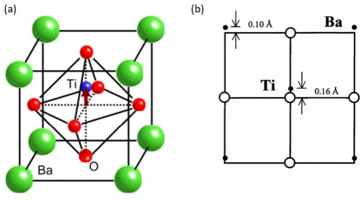
[image:25.595.144.511.303.507.2]With a tolerance factor of 1.06, BaTiO3 has a typical perovskite structure with a tetragonal distortion, space group P4mm (No. 99) as shown in Figure 1. 7 (a).
Figure 1. 7: Displacement of the A and B cations in BaTiO3. Green spheres represent the A cations (Ba),
the blue sphere represent the B cation (Ti), and red spheres represent oxygen anions in octahedral coordination (Tazaki et al 2009).
Ferroelectricity arises by Ti off-centering, generating distortion and the appearance of spontaneous polarization in the material.
material. At this temperature, dielectric permittivity presents a maximum value (Jona & Shirane, 1962).
Figure 1. 8: The temperature dependence of the dielectric constant for BaTiO3 and the various phase
transitions (Ito & Uchino, 2005).
Lead titanate, PbTiO3, is also a well-known ferroelectric perovskite oxide (Arlt, 1990; Jaffe et al., 1971; Moulson & Herbert, 1990). The ferro- to paraelectric phase transition occurs at higher temperature than BaTiO3, around 490ºC (Sani, Hanfland, & Levy, 2002). This compound presents tetragonal structure (P4mm) at room temperature and it is characterised as having high tetragonal distortion with c/a value of 1.064 (BaTiO3, c/a=1.01) (Cohen, 1992). The high tetragonality of this structure suggests a remarkable displacement of the cations, generating the appearance of a dipole moment in the direction of this axis (Rabe & Ghosez, 2007).
(ii) Lone pair electrons
BiFeO3 is possibly the only material that is both magnetic and a strong ferroelectric at room temperature and it was one of the first multiferroic materials with perovskite structure to be studied.
BiFeO3 exhibits a rhombohedral structure (point group R3c) at room temperature
Ferroelectricity in BiFeO3 is originated by the lone pair electrons (s2) of Bi3+, which shifts Bi+3 to give rise to a spontaneous polarization along the [111] direction (Catalan & Scott, 2009). The lone pair is visualized by red surface in Figure 1. 9.
Figure 1. 9: Schematic representation of BiFeO3 showing that the lone pair (red surface) promotes the
appearance of spontaneous polarisation (Fiebig, Lottermoser, Meier, & Trassin, 2016).
(iii) Geometry
Other mechanism that generates ferroelectricity is due to geometric factors (Spaldin, 2017). Spontaneous polarisation in hexagonal RMnO3 (where R= Sc, Y, In or Dy) compounds arises from a tilt and deformation of MnO5bipyramids, which shift the rare-earth ions as pointed by the arrows on Figure 1. 10.
Figure 1. 10: Schematic representation of YMnO3. Spontaneous polarisation (P) arises when the MnO5
(iv) Charge ordering
Furthermore, the occurrence of ferroelectricity in LuFe2O4 is explained by other mechanism, charge-ordering (Ikeda et al., 2005). Fe2+ and Fe3+ ions are arranged in alternating chains in a superlattice. Thespontaneous polarization arises between the two layers (Figure 1. 11).
Figure 1. 11: Charge ordering is the source of an electric polarization in LuFe2O4, which is illustrated in
this figure. Green, grey and red sphere represent Fe+2, Fe+3 and O, respectively. (Fiebig et al., 2016)
Finally, an alternative way to induce ferroelectricity is the magnetic order. Spin interactions can drive to a non-polar state and it is related to the generation of multiferroicity (Cheong & Mostovoy, 2007; Mostovoy, 2006).
1.2.4. Piezoelectricity in ferroelectrics
The direct piezoelectric effect (Equation 1.5.) relies on the accumulation of electric charge density (D), which is generated by an applied mechanical stress (T). On the other hand, the indirect piezoelectric effect (Equation 1.6) occurs when an electric field (E) is applied on solids and causes stress, and consequently, a proportional strain (S). The basic relationships between the electrical and elastic properties can be represented as follows:
𝐷 = 𝑑 · 𝑇 + 𝜀 · 𝐸 Eq. 1.5
𝑆 = 𝑠 · 𝑇 + 𝑑 · 𝐸 Eq. 1.6
Where d, s and 𝜀 are the piezoelectric charge coefficient, compliance coefficient and the permittivity characteristics of each material, respectively.
Figure 1. 12 shows an illustration of a strain (S) versus electric field (E) curve for ferroelectrics. The shape looks like a butterfly, and it is usually known as the “butterfly loop”.
Figure 1. 12: Typical strain- electric field response curve for a ferroelectric material.
Firstly, strain increases with electric field (A). The dipoles of all the grains start to align with the electric field and the ceramic expands through the piezoelectric effect. The expansion continues until the maximum field is reached. When the field changes orientation, strain decreases more slowly due to the reoriented dipoles (B). As the field becomes negative the dipoles are forced away from their original orientation. At the critical point, the field is large enough to switch the direction of polarization (C). After polarization reversal (D), the crystal expands again until it reaches its physical strain limit. The electric field is again reversed, and the line E-F-G is analogous to that explained for B-C-D in the other direction.
Among solid solutions with perovskite structure, a type of ferroelectric systems has emerged that have a morphotropic phase boundary (MPB). An MPB is defined as the compositional barrier between two phases, in a phase diagram with identical Gibbs energy (Cao & Cross, 1993)
This phenomenon occurs in a solid solution between compounds that have different polymorphs derived from the perovskite structure. With the increase of substituted cations in the solid solution, the crystal structure of the solvent phase is distorted and a transition to the other polymorph happens. That composition or range of compositions in which the phase transition appears, is known as MPB.
of solute until it reaches the MPB. In this region, it is observed that electrical properties have a tendency to increase, achieving maximum values in parameters such as dielectric constant, piezoelectricity, electromechanical properties, spontaneous polarization and pyroelectric coefficient (Bhalla et al., 2000).
[image:30.595.249.396.343.512.2]One of the most investigated solid solutions that presents this phenomenon is x PbTiO3 - (1-x) PbZrO3 (PZT). This ferroelectric system exhibits the highest piezoelectric coefficients known in the MPB region (x ~ 0.47). Controversy about the origin of the high piezoelectric response in the MPB is found in the literature. Finally this behaviour in PZT was explained by Guo et al. in 2000 through the presence of a phase with monoclinic structure (space group Cm), which is considered intermediate between rhombohedral and tetragonal. Modifications on PZT phase diagram, after the discovery of the monoclinic phase is shown in Figure 1. 13.
Figure 1. 13: PZT phase diagram around the MPB showing the monoclinic region (Guo et al., 2000)
The electrostrictive effect is the non-linear deformation of a solid under an electric field (E). The induced strain (S) is proportional to the square of electric field (E) and it is expressed in the following Equations 1.7-8:
𝑆 = 𝑄 · 𝑃2 Eq. 1.7.
𝑆 = 𝑀 · 𝐸2 Eq. 1.8
Figure 1. 14: Electric field dependence of the strain in a PMN single crystal at various temperatures. (Nomura & Uchino, 1982).
PMN electrostrictive ceramics belong to a class of relaxor ferroelectrics, materials which shows a strong dispersion of dielectric permittivity. TC can vary in a temperature interval of hundreds of degrees and the dielectric peak is broader than for normal ferroelectric (Figure 1. 15). However, the mechanism for this effect is still an open question (Cowley, Gvasaliya, Lushnikov, Roessli, & Rotaru, 2011).
Figure 1. 15: Temperature dependence of the real part of the dielectric permittivity ε´ of PMN (Smolenskii, 1970).
1.2.5. Literature review of KNbO3
the KN crystal symmetry can be described with orthorhombic structure (space group Amm2). The orthorhombic Amm2 cell contains two KNbO3 units and the lattice parameters are a = 3.973 Å, b = 5.695 Å and c = 5.721 Å (Hewat, 1973).
Shirane et al reported in 1954 a value of 41 2 µC/cm2 for the spontaneous polarisation of KN single-domain at room temperature. This large value is due to cation displacement of Nb+5 within the NbO6 octahedra. The distortion is generated by the hybridisation of the empty d-orbitals of Nb+5 with the O2- p-orbitals.
Figure 1. 16 (a) and (b) shows the dielectric constant dependence with the temperature in a KN crystal (Shirane et al., 1954) and a ceramic (Birol, Damjanovic, & Setter, 2005) respectively. The Curie temperature of both, crystal and ceramics, for KN is about 410ºC. At −55 °C the crystal symmetry changes from rhombohedral (R3m) to orthorhombic (Amm2) and at 220 °C from orthorhombic to tetragonal (P4mm). The ferroelectric phase transition behaviour for KN single crystal and ceramic are analogous to BaTiO3 (Figure 1. 8).
Figure 1. 16: Evolution of the dielectric constant with the temperature in (a) a single crystal (Shirane et al., 1954) and. (b) a ceramic (Birol et al., 2005) of KN. Dielectric anomalies are related with the phase transition.
Figure 1. 17: Raman spectra of KNbO3. The temperature and the corresponding crystal phase are indicated
for each spectrum (Baier-Saip et al., 2005)
The cubic phase displays two large and broad bands. These bands persist in the tetragonal and orthorhombic phases, and they split in narrower modes, which become sharper as temperature decreases. Extra modes emerge in orthorhombic and rhombohedral phase. The intensity of the sharp mode near 192 cm-1 increases systematically with the decrease in temperature. Detailed description of Raman modes in KN will be given in Chapter 3.
Figure 1. 18: The mechanical coupling factor in KN single crystals. The angle θ specifies the rotation away
from the polar axis of the pseudocubic system. The largest KT (0.69) value is obtained at 40.51º (Rödel et
al., 2009).
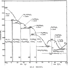
The preparation of KN by conventional ceramic processing is challenging because of different issues. The evaporation of potassium during the heat treatments of the synthesis and sintering prevent KN ceramics from being fully densified. When the ratio K/Nb differs from unity, an unstable secondary phase, K4Nb6O17 (or 2K2O-3Nb2O3) is easily formed. This phase affects the stability of the KN ceramic when exposed to humid environment. Furthermore, other problem that affects the KN preparation is its low melting point (1039 ºC) which is very close to the sintering temperature, as shown by the Reisman and Holtzberg’s phase diagram (Figure 1. 19). These problems are approached in Chapter 3.
Figure 1. 19: Phase diagram of Nb2O5-K2CO3 system. The melting point of KN is indicated at
However, Birol et al. achieved to prepare KN ceramics with high relative density (93.9%) after firing the green bodies at 1035 ºC in oxygen. The same study shows hysteresis loop of KN at room temperature (Figure 1. 20 (a)). The ceramic was able to withstand an electric field of 80 kV/cm and exhibited a maximum spontaneous polarisation value of 25 µC/cm2 and a coercive field of 15 kV/cm. Kakimoto et al obtained a density of 4.49 g/cm3 (97.4%) for KN ceramics which were sintered at 1020 ºC in a potassium rich atmosphere provided by covering the green body with additional KN powder. This study also reported an enhancement of the ferroelectric properties for (1-x) KNbO3-x LaFeO3 (Figure 1. 20 (b)) with increasing x content.
Figure 1. 20: Hysteresis loop of polycrystalline KN ceramic at room temperature reported by (a) Birol and
(b) (1-x) KNbO3-x LaFeO3 Kakimoto et al.
1.2.6. Applications of piezo- and ferroelectrics
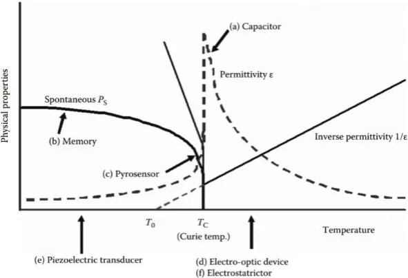
[image:36.595.178.474.277.479.2]This section provides a general overview about piezo- and ferroelectric applications without going into many details. From their discovery to the present, FE materials have been implemented in wide range of applications. Depending on the application ferroelectrics can be prepared as bulk ceramics or thin films. Figure 1. 21 illustrates the temperature dependence of the spontaneous polarisation (Ps), dielectric constant (ε) and its inverse (1/ε). Schematically the classic applications of ferroelectrics are indicated in this graph in function of the physical properties required and the operational temperature.
Figure 1. 21: Spontaneous polarization, permittivity and inverse permittivity in a ferroelectric material. (a)– (f) indicate the temperature ranges for each application (Uchino, 2009).
Capacitors (a) need to be easily polarised under an electric field, then they will work in the maximum value of dielectric constant close to the transition (Tc). In memory devices (b) the materials must be FE at RT. Pyroelectric sensors (c) are based on the large temperature dependence of the spontaneous polarisation below TC.
signal transmission or to charge up batteries for portable electronics (Mitcheson, Yeatman, Rao, Holmes, & Green, 2008). The indirect piezoelectric effect is used in actuators to generate a force, vibration or an acoustic wave. Both effects can be employed in a device to combine actuation and sensing. Finally, TC for electro-optic (d) and electrostrictive (f) devices are lower than RT to use their paraelectric state.
1.3. Photoferroelectrics
1.3.1. Electronic band structure of solids
A solid is a set of ions and electrons at different energy levels in thermodynamic equilibrium and its band structure gives the allowed and forbidden energy ranges that an electron can have within the solid and consequently informs of many physical properties.
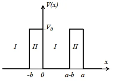
In quantum mechanics, a Hamiltonian (H) is a mathematical operator that corresponds to the total energy in a system. Taking in consideration all the ionic and electronic interactions into the solid, the formulation of the Hamiltonian becomes very complex. In order to make this task easier some approximations are considered: (i) ions are at rest, then ion’s kinetic energy term is zero; (ii) ions are fixed, interaction ion-ion term is discarded; and (iii) each electron does not perceive an individualized interaction of each ion and electron, but a resulting effective potential generated by all electrons and ions, 𝑉(𝑟𝑖).
Considering the previous approximations for the Hamiltonian, the evolution over time of an electron is given by the Schrödinger equation (Eq. 1.9).
Η̂𝜓(𝑟, 𝑡) = ∑ {− ℏ
2
2𝑚∇𝑖 + 𝑉(𝑟𝑖)} · 𝜓𝑖(𝑟𝑖, 𝑡)
𝑖
Eq. 1. 9
The first term represents the kinetic energy of the electrons, where 𝑖 is the number of electrons, 𝑚 is the electron mass, ℏ is the Planck constant (6.58212·10-16 eV·s/rad), ∇𝑖 is the gradient operator and 𝜓𝑖(𝑟𝑖, 𝑡) is the electron wave function. The resulting effective potential (𝑉(𝑟𝑖)) is assumed to be a periodic potential of period a and consisting of an
Figure 1. 22: Schematic representation of idealized quantum-mechanical system that consists of an infinite periodic array of rectangular potential barriers.
The solution of the Schrödinger equation for this model is given by the Bloch functions. A 1 dimensional chain of atoms (x direction) separated by a lattice spacing a, is considered (Eq. 1.10).
Ψ(𝑟𝑥) = 𝑢(𝑟𝑥) · 𝑒𝑖𝑘𝑟𝑥 Eq. 1.10
The wavefunction Ψ(𝑟𝑥) is a combination of the periodic potential 𝑢(𝑟𝑥) of each atom with an exponential term that varies with the wavenumber 𝑘. The wavefunction is continuous and periodic (Eq. 1.11).
Ψ(𝑟𝑥) = Ψ(𝑟𝑥+ 𝑎) Eq. 1.11.
It is convenient to work with wavenumbers, k, instead of time to approach the Schrödinger equation, because k always presents discrete values (Eq. 1.12).
𝑘 = (2𝜋 𝑎 ) 𝑛
Eq. 1.12
Where n is an integer number.
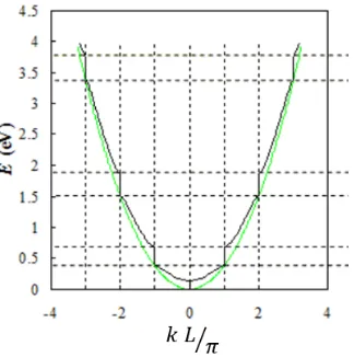
Figure 1. 23: Representation of the band structure E(K). Black curve is the solution assuming a periodic potential (Model Kroning-Peney). and green curve is for a free electron model.
Figure 1. 24: Energy (E) versus momentum (k) plot. Schematic representation of direct and indirect band-gaps.
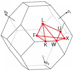
However, real band structure in solids must consider orbital interactions in 3 dimensions arising from s, p, d, and f orbitals on each atom. This leads to complex energy diagrams with many bands.Thus, the calculation of E(k) is unfeasible and requires computational programs. Extending the system to 3 dimensions, the k vectors comprise the first Brillouin zone of the crystal. Before going deeper in this, it is necessary to explain some crucial concepts. Due to the periodic properties of the lattice and the Bloch functions, every k vector in the real space is equivalent to a k vector inside this Brillouin Zone (also called k-space). Figure 1. 25 shows the Brillouin Zone of a face-centered cubic (FCC) lattice where b1, b2, and b3 are the reciprocal vectors and the red points labelled (Γ, L, K, W, X, U) correspond to high symmetry points in the Brillouin Zone.
Figure 1. 25: The Brillouin zone of FCC lattice showing the reciprocal vectors and the high symmetry lines and points.
band diagrams of (a) GaAs (direct band-gap) and (b) Si (indirect band-gap) which are the preferred materials for conventional solar cells. The band-gaps are 1.43 eV and 1 eV, respectively.
Figure 1. 26: Electronic band structure of (a)GaAs, which exhibits direct band-gap (1.43 eV) and (b) Si with an indirect band-gap of 1 eV.(Rohlfing, Krüger, & Pollmann, 1993).
1.3.2. Photovoltaic effect
As mentioned previously, semiconductors exhibit band-gaps of ~1eV which promotes the absorption of sunlight due to the matching in energy with the solar spectrum, which mostly emits in the visible range (400-700 nm). When the light is absorbed by a semiconductor material, photons transfer the energy to the valence electrons producing the excitation of these from the VB to the CB. This process creates holes in the VB and electrons in the CB (electron-hole pair). After some time, electrons go back to their original electronic state, emitting photons or phonons. This procedure is called recombination. However, if there is an electric potential across the material, it will promote a net flow of photogenerated electrons and holes (photocurrent). The creation of electric current in a material under sunlight illumination is what is known as ‘photovoltaic effect’.
with phosphorous and boron. This procedure generates an intrinsic electric field (p-n junction) in the material that separates the photocarriers.
The power conversion efficiency (𝜂) of incident light power (𝑃𝑖𝑛) to electricity is proportional to the open-circuit voltage (𝑉𝑜𝑐), short-circuit current (𝐽𝑠𝑐) and to the fill-factor (FF) is given by Eq. 1.13.
𝜂 =𝑉𝑜𝑐𝐽𝑠𝑐𝐹𝐹 𝑃𝑖𝑛
Eq. 1.13.
The maximum voltage which can be generated by conventional semiconductors (𝑉𝑜𝑐) is
[image:42.595.241.412.391.526.2]limited by the band-gap of the material. The photocurrent (𝐽𝑠𝑐) is measured when 𝑉𝑜𝑐=0 and it is determined by the portion of solar spectrum that the material absorbed. In an ideal solar cell, the power generation would be equal to the product 𝐽𝑠𝑐·𝑉𝑜𝑐. Real solar cells show a different maximum power point (MPP) (Figure 1. 27). To evaluate the quality of a solar cell the fill factor (FF) is calculated, which is given by the ratio of the products of the current and the voltage at MPP and of 𝑉𝑜𝑐 and 𝐽𝑠𝑐.
Figure 1. 27: Photovoltaic characteristic curve(I-V). Green square represents the ideal conversion power in a solar cell and the red one the real maximum power. The relation of this quantities gives the fill factor (FF).
In academia, photoferroelectrics are presented as potential candidates for using in photovoltaic devices due to their anomalous photovoltaic response that will be detailed in the next section. Anyway, these materials do not appear in the NREL chart because of their extremely low efficiency.
Figure 1. 28: NREL chart show cells efficiencies from 1975 to 2017.
1.3.3. The anomalous photovoltaic effect in ferroelectrics
1.3.3.1. Introduction
Anomalous photovoltaic effect in polar materials was discovered in early 70’s (V. M. Fridkin et al., 1974; Grekov, Malitskaya, Spitsina, & Fridkin, 1970). The first explanation of the photovoltaic effect based on the asymmetry of Fe+2-doped LiNbO3 was reported by Glass in 1974. Since then, photo-response on thin films of classical ferroelectrics have
Different explanations have been proposed to explain the nature of anomalous photovoltaic effect in polar materials. However, all have one point in common: photo-response in ferroelectric is generated by completely different mechanism than observed in non- polar structures such as p-n junctions.
Photovoltages in ferroelectrics can exceed several times their band gaps values, in contrast to conventional semiconductors. Spontaneous polarisation in non-centrosymmetric materials provides an alternative way to separate the photoexcited carriers.
1.3.2.2. Origin of the photoresponse in ferrolectrics
As was introduced, the origin of the bulk photovoltaic effect (BPE) was explained for first time more than 40 years ago (Glass, von der Linde, Auston, & Negran, 1975) and it has been recently reviewed in BaTiO3 thin films (Zenkevich et al., 2014).
The microscopic mechanism that promotes BPE in Fe doped LiNbO3 was directly related to asymmetric scattering of excited electrons, in this case due to the ‘iron defects’ (Glass et al., 1975). When some lithium cations (Li+1) are substituted by iron cations (Fe+2) in a LiNbO3 array, the results are that the potentials barriers for electrons are not equal in all directions (Figure 1. 29(a)). If an electron is excited from the ground state (E0) to an energy level E1, the electron remains trapped in the potential well. Nevertheless, if the electron is excited to E2 level then it will be scattered in a certain direction. Always there is a preferred orientation from a statistic point of view (possible tunnelling) which leads to the presence of more electrons with certain momentum vector value, k. This imbalance gives rise to the appearance of a net flow of electrons in the same direction. These electrons will travel 𝑙0 distance in space before losing their energy and decay to the lowest
Figure 1. 29: (a) Asymmetric potential well which leads the asymmetric scattering of the excited electrons (Butler, Frost, & Walsh, 2015)(b) While photoelectrons in a centrosymmetric crystals (i) present an homogeneous momentum distribution, in a noncentrosymmetric crystal (ii) a photocurrent appears under illumination due to the asymmetric momentum distribution (Zenkevich et al., 2014a).
However, noncentrosymmetric materials without impurities also exhibit photoresponse under illumination. Fridkin explained in his book ‘Photo-ferroelectrics’ (1979) in a contrived manner and difficult to understand that there are several microscopic mechanisms that can contribute to the photocurrent such as impurity centres and photoinduced fluctuations. In subsequent works, Fridkin directly attributed ‘the violation of the principle of the detailed balancing for photoexcited (non-equilibrium) carriers in noncentrosymmetric crystals’ to the generation of photocurrent. This mechanism would be analogous to the Glass model (explained above) but without making clear the origin of asymmetric scattering of excited electrons.
1.3.2.3. Experimental measurements
The photoresponse in ferroelectrics is measured in the same way as conventional photovoltaics. A homogeneous polar medium with short-circuited electrodes is uniformly illuminated, thus the photocurrent (JSC) is generated. On the other hand, the photovoltage
Figure 1. 30: Schematic representation of measurements of the photovoltaic current J and photovoltage Uph
Initially, the Glass model considered that the photovoltaic current was proportional to the intensity of the monochromatic incident light (Eq. 1.14).
𝐽𝑠𝑐 = 𝜅1𝛼𝐼 Eq. 1.14
where 𝛼 is the absorption coefficient and 𝜅1 is a coefficient that relies on the nature and concentration of the impurity centres and the energy of the incident photons. Afterwards quantum mechanics was incorporated to this model for describing the asymmetric scattering of excited electrons in ferroelectrics (von Baltz & Kraut, 1978). However, this model did not consider the dependence of photocurrent with the rotation of the polarization of the incident light. Hence, the expression of the photocurrent was described with a third rank tensor (Eq. 1.15) (V. M. Fridkin, 2001; Kraut & Von Baltz, 1979; Sturman & V. M. Fridkin, 1992; Von Baltz & Kraut, 1981).
𝐽𝑆𝑐𝑖 = 𝛼𝛽𝑖𝑗𝑙𝑝𝑗𝑝𝑙𝐼0 Eq. 1.15 where 𝑝𝑗 and 𝑝𝑙 are the components of the light polarization vector, 𝐼0 is the amplitude of the light and the scalar value of the tensor 𝛽𝑖𝑗𝑙 expressed in terms of microscopic
quantities is given by Eq. 1.16.
𝛽 =𝑒 𝑙0𝜉𝜑 ℏ𝜔
Eq. 1.16
where e is the elementary charge of the electron, 𝑙0 is the shift of excited electrons, 𝜑 is the quantum yield, ℏ𝜔 is the energy of the photons and 𝜉 is a parameter that characterises the shift of the electrons in an anisotropy direction.
explained later (Zenkevich et al., 2014). Until few years ago, the highest efficiency (0.28%) among FEs materials was reported in La-doped PZT thin film (Qin, Yao, & Liang, 2008).
Different studies showed that if the thickness of the polar materials, l, is in the same order of magnitude or less than the shift in the nonthermalized electrons l0, the photoinduced
electric field and the conversion efficiency become much higher.
Zenkevich et al. reported a greatly enhancement of photoinduced electric field (EPV) when
the thickness of the BaTiO3 films was reduced to few tens of nanometres. Figure 1. 31 shows the I-V measurements for 50-nm (a) and 20-nm (b) BaTiO3 films at different illumination intensities. UPV values are practically equal to both thicknesses.
Consequently the EPV values surpass by 4 orders of magnitude those reported for the bulk
crystals (Sturman & V. M. Fridkin, 1992).
Figure 1. 31: Photocurrent at different light intensities (1: dark current; 2: I = 1.5×10⁻¹ W/cm2; 3: I =
3×10⁻¹ W/cm2; 4: I = 4.5×10⁻¹ W/cm2; and 5: I = 7.5×10⁻¹ W/cm2) measured on two thin-films of
thickness: (a) l = 50 nm and (b) l = 20 nm in Pt/BaTiO3/Pt sample.
However, Yang et al. described a new mechanism for explaining the nature of the photovoltaic effect in BiFeO3 thin film and completely refused the BPE detailed above. Linear increase of the photovoltage was observed with the increase of electrode spacing,
Figure 1. 32: Evolution of VOC versus electrode spacing (inset) for four t samples of high purity BiFeO3
film with different thicknesses of 100 nm (red), 200 nm (blue) and 500 nm (green) and monodomain (black)(Yang et al., 2010).
The new mechanism proposed for the photovoltaic effect in BiFeO3 thin films is related with the presence of the 71° (Figure 1. 33 (a)) and 109° domain walls. Separation of photoexcited carriers occur at the ferroelectric domain walls, where the gradient of polarisation gives rise to an internal electric field. Then photoelectrons move to one side of the wall while holes move to the other side (Figure 1. 33 (d)). Indeed, an accumulation of charges is created close to the domain wall under illumination. Figure 1. 33 (b) and (c) show the band diagrams under dark and illumination conditions. So, the net photovoltage is generated across all the sample, resulting from the combined effect of the domain walls and the excess charge created by illumination.
Figure 1. 33: (a) Schematic illustration of ferroelectric domains and 71º domain walls in BiFeO3. (b) Band
Even if the separation of the carriers at the domain wall is quite similar to the separation at the p-n junction, the main difference resides in the magnitude of the electric field that drives the charge separation, conventional Si systems exhibit 7 kV/cm compared with BiFeO3 that presents 50 kV/cm.
However, this model has created controversies in the literature, indeed several studies clearly validated both models (Alexe, 2012; Alexe & Hesse, 2011; Bhatnagar, Ayan, Young, Hesse, & Alexe, 2013; Ji, Yao, & Liang, 2011).
In conclusion, the origin of the photocurrent is not generally understood, and it is even difficult to determine whether the effect is due to BPE or domain wall mechanism.
1.4. Band-gap engineering
To enhance the photovoltaic efficiency, the band-gap of ferroelectrics (FE) must be narrowed while maintaining their polar nature. Indeed, band-gaps of FE usually present values above 3 eV (Table 1. 3), which limits their light absorption mostly to the ultraviolet (UV) region that it is equivalent to absorbing only 8% of the solar spectrum. The wide optical bandgaps in oxide FE perovskites arise from the nature of the bonding between O and B ions. Indeed, the large differences in electronegativity between the O and the B ions lead to the valence band to be formed by the 2p O states and the conduction band by the d states of the B transition metals sitting within the O octahedra.
Ideally, a photovoltaic material should have a band gap in between 1.0–1.8 eV in order to match with the maximum emission of the solar spectrum which is the visible range (400-800 nm).
FE material Band-gap (eV) Reference
BaTiO3 3.34 (Wemple, 1970)
PbTiO3 3.88 (Zelezny et al., 2016)
LiNbO3 3.78 (Dhar & Mansingh, 1990)
KNbO3 3.24 (T. Zhang et al., 2013
BiFeO3 2.67 (Hung et al., 2012)
In this section, two strategies and several studies on bandgap engineering in ferroelectrics are described.
First approach to narrow the band-gap is by controlling the chemical order of the species. As shown on Table 1. 3, BiFeO3 exhibits the narrowest band-gap (2.67 eV) among ferroelectrics. However, it is only able to capture 20% of the solar spectrum. The modification of Fe/Cr cationic order into parent BiFeO3 has been related with lower band-gaps. Theoretical studies predicted a band gap range of 1.4–2.0 eV in BiFe0.5Cr0.5O3 (BFCO) compounds(Zhao, Wen, Wang, Guan, & Liu, 2008), and it was experimentally validated by Nechache et al. in 2011. In this study, a PV power conversion efficiency of 6.5% for red laser was reported in BFCO thin films with a photovoltaic current density of 0.99 mA cm−2, one of the largest recorded at the time. More recently, the same authors obtained an efficiency of 8.1% for optimised multilayer system of BFCO (Figure 1. 34 (a)), the highest efficiency ever recorded on conventional ferroelectrics. Each layer absorbed a different part of the solar spectrum. The tunability of the bandgap in each layer arises from the interaction between Fe and Cr with different oxidation states, alternating at B sites of the perovskite. By inspection of Figure 1. 34 (b) the band-gaps are determined from 1.4 to 3.2 eV (from 885 to 388 nm) which covers wide range of solar spectrum.
Figure 1. 34: (a) Illustration of the tested BFCO multilayer structure. (b) (αE)2 as a function of photon
energy, in arbitrary units (a.u.).
Second route to reduce the band-gap would be chemical engineering. Indeed, solid solutions permit the properties of different compounds to be adapted.
This thesis is devoted on band-gap engineering for solid solutions based on KNbO3.
[image:51.595.121.552.344.550.2]Different electronic band diagrams of KNbO3along the symmetry lines of the Brillouin zone are shown in Figure 1. 35. Both, Okoye and Sinha et al. calculations are in agreement for cubic KNbO3, as shown in Figure 1. 35 (a) and (c). The indirect band gap appears between the top valence band at the R point and the bottom of the conduction band at the Γ point. However, Xu et al reported that KNbO3 exhibits the valence-band maxima at R points and the conduction-band minima at G points, indicating again indirect band-gap (Figure 1. 35 (b)). In contrast, Modak & Ghosh obtained direct band-gap (Figure 1. 35 (d)). Table 1. 4 and Table 1. 5 show theoretical and experimental band-gap values for KN reported in literature.
Figure 1. 35: (a), (b), (c) and (d): Different models for the electronic band structure of cubic KNbO3 along
Methods Band-gap (eV) References
Direct Band-gaps
LDA 1.98
(Fenggong Wang & Rappe, 2015; Xu, Wu, Zhang, Wu, & Ding,
2017a)
PBE 1.98
HSE06 3.83, 3.10
GWO 3.89
FPLAP 1.58
Indirect Band-gaps
LDA 1.43
PBE 1.42
HSE06 3.24
GWO 3.28
Table 1. 4: Calculated direct and indirect band-gaps gaps of KNbO3 with LDA, PBE, HSE06, and GW0.
Methods Band-gaps References
Absorbance Spectroscopy
3.24 (T. Zhang et al., 2013) 3.14 (Liu, Chen, Li, & Zhang, 2007) Ellipsometry
spectroscopy
3.95 (Tyunina et al., 2015) 3.80 (Ilya Grinberg et al., 2013) Diffuse reflectance
spectroscopy 3.10
(Eng, Barnes, Auer, & Woodward, 2003)
Table 1. 5: Experimental band-gaps of KNbO3, measured by absorbance, ellipsometry and diffuse
reflectance spectroscopy. Authors do not differentiate between direct and indirect band-gaps.
[image:52.595.115.541.73.282.2]Figure 1. 36: (a) Ferroelectric loops for a thick film KN-BNN x=0.01 at 10-7 torr and 77–170K (b) Ellipsometry measurements for KN-BNN x=0.0–0.5 reveal a bandgap narrowing from 3.8 eV to 1.18 eV (I. Grinberg et al., 2013)
Consequently, this composition, KN-BNN, has been largely investigated in the last four years. Two studies reported similar band gap narrowing in the ceramic KN-BNN system and both showed the lowest band-gap (1.18 eV) corresponds to x=0.2 (Figure 1. 37 (a) and (b)) (Song et al., 2017). It was also suggested that KN-BNN exhibits ferromagnetism at RT which would offer great potential in multiferroic applications (Zhou, Deng, Yang, & Chu, 2014).
Figure 1. 37: :(a) Absorption spectra and (αhυ)2versus hυ (inset) of KN-BNN bulk ceramics (x=0, 0.1 ,0.2,
0.3) (Zhou et al., 2014) (b)(αhυ)2versus photon energy in KN-BNN (x=0, 0.1 ,0.2, 0.3, 0.4 and 0.5) bulk
ceramics sintered by solid stat reaction (Song et al., 2017) Both show the narrowest ban-gap (~1 eV) for
x=0.2.
Zhang et al reported a narrow band-gap (up to 1.39 eV) and P-E loop (Pr =1.4 C/cm2) in
Figure 1. 38: (i) (a) Absorption spectra and (b) absorption coefficient square (𝛼ℎ𝜐)2vs. Photon energy
(h) plots of KN-BNN films deposited at different O2 pressures. (c) The bandgap of the films as a function
of the Ni content. (ii) P-E loops for KN-BNN thin films deposited at O2 pressures of 0.01, 0.1, and 0.5 Pa.
Bai et al studied optic and ferroelectric properties of KN-BNN bulk ceramic with x=0.01, stoichiometric (CI) and non-stoichiometric (CII) created by a potassium deficiency. Figure 1. 39 (a) and (b) illustrate absorbance and photon energy for both materials. The authors affirmed that measuring absorbance (Figure 1. 39 (a)) is not a reliable method to determine the band-gap in solid samples. Then they decided to measure diffuse reflectance and to plot the function (F(R)·hv)2 (being F(R) Kubelka-Munk formula) to determine the band-gaps of KN-BNN (Figure 1. 39 (b)). The samples CI and II exhibit band gaps of 1.40 eV and 1.48 eV, respectively. Worth to mention, the sample CI was able to withstand an electric field up to 80 kV/cm (Figure 1. 39 (c)).
Figure 1. 39: (a) Absorption spectra and (b) (F(R) hυ)2 versus hυ for KN-BNN (x=0.01) bulk ceramic (C1
[image:54.595.116.556.69.276.2]Very recently, a study has been published by the same author (Bai, Tofel, Palosaari, Jantunen, & Juuti, 2017) that compares (K0.5Na0.5)NbO3 (KNN) and 0.98 (K0.5Na0.5)NbO3- 0.02 Ba(Ni0.5Nb0.5)O3 (KNN-BNNO) ceramics. This last compound revealed large ferroelectric (26 µC/cm2) and piezoelectric (100 pm/V) properties (Figure 1. 40 (b)) accompanied with a surprising narrow bandgap (1.6 eV).
Figure 1. 40: (a) Absorption spectra and Tauc plot of the thick-film KN-BNN. (b) Ferroelectric loop for KN-BNN ceramic and thick-film. (Bai, Siponkoski, et al., 2017)
However, contradictory results for KN-BBNZ band gap are found in literature. (Zhou, Deng, Yang, & Chu, 2016). Figure 1. 41 (a) illustrates the absorption spectra and the
(F(R) hυ)2 versus the photon energy of KN-BNN thin film. The two slopes pointed at 1.85 eV (2) and at 2.51 eV (1), are attributed, respectively, to intraband transition of Ni 3d orbitals and band-to-band transition from hybridized Ni 3d and O 2p to Nb 4d states Figure 1. 41 (b).
Figure 1. 41: (a) Absorption spectra of the KN-BNN film on Pt(111)/Ti/SiO2/Si(100) substrate and a plot
of (F(R) hυ)2 as a function of hυ (inset). (b) A schematic illustration of intraband electronic transition in
Moreover, Wu et al. synthesised KN-BNN (0≤x≤0.4) nanocrystals fabricated by sol-gel based on Pechini method and showed that Ba and Ni modifications slightly narrow the original band-gap of KN, only 0.15 eV smaller than KN (Figure 1. 42 (b)). Three broad absorption bands (beside the band-gap) can be found in the absorbance spectra at 450 nm (2.75 eV), at 720 nm (1.72 eV) and at 1150 nm (1.07 eV) (Figure 1. 42 (a)). and attributed to d-d transitions created by Ni+2 ions in the crystal of KN-BNN. Authors concluded that previous reports which gave band gap values of 1.1-1.5 eV of KN-BNN may be misinterpreting the 720 nm absorption band in KN-BNN as the intrinsic band-gap absorption
Figure 1. 42: Absorption spectra of KNbO3 (x = 0) and KN-BNN (x = 0.1–0.4); (b) plots of (F(R) hυ)2-hυ
(inset). (Wu et al., 2016)
These studies gave a boost to develop theoretical and experimental works based on the band-gap tunability of the compounds based on KN. Systematic band-gap narrowing was reported in different solid solutions based on KN, such as (1-x) KNbO3-x Ba(Co0.5Nb0.5)O3-δ (KBCNO) which shifts down to 2.4 eV (Limin Yu, Jia, Yi, Shan, & Han, 2016). Very recently systems that has been studied include KNb1-xFexO3− δ (Nie et al., 2017) and (1-x) KNbO3-xBa(Nb0.5Fe0.5)O3 (KBNFO) which show a reduction of the band gap from 3.2 eV down to 1.74 eV (Lu Yu, Deng, Zhou, Yang, & Chu, 2017).
1.5. Motivations
polarization switching and can also trap the photo-excited carriers and consequently increase the charge recombination rate. Hence, oxygen vacancies are detrimental to ferroelectric and photovoltaic properties. First principle calculations estimated the bandgaps and spontaneous polarisation for vacancy-free KNbO3 co-doped with Zn+2 in B-site and A1+2 and A2+3 substitution on the A-site (A1+2= Pb2+, Ba2+, Sr2+; A2+3= La3+, Bi3+) in order to achieve charge neutrality. The calculated band-gaps for these systems present values between 2.92 eV and 2.11 eV (F Wang, Grinberg, & Rappe, 2014).
This motivates us to investigate alternative strategies to lower band-gap while preserving ferroelectricity and without creating oxygen vacancies. The approach to reduce the band-gap of parent KN in this work relies on replacing Nb5+ cations by lower valence transition metals (Me3+)dopants. The transition metals were selected following the periodic table order (Mn, Fe, Co and Ni). Furthermore K+1 will be substituted by Bi+3 in order to maintain the compositions stoichiometry. The mechanism which leads to the band-gap narrowing is the repulsion between non-bonding 3dn orbitals of the Me3+ and 2p6 orbitals of O2- upshifting the VBM.
1.6. Aims and Objectives
1.6.1. Aims
1.6.2. Research objectives
To address the key aims, this research has the following objectives:
To determinate the current state of the art knowledge in photo-ferroelectrics and band-gap engineering in ferroelectrics oxides.
To develop a strategy to narrow band-gaps in FE, avoiding oxygen vacancies.
To prepare bulk ceramics by solid state reaction for all the systems explored in this work and to optimise their processing.
Experimental validation of theoretical predictions and controversies in the literature.
To investigate the impact of BiMeO3 (with Me= Mn, Fe, Co and Ni) doping on the structure, dielectric, ferroelectric and optical properties of KNbO3.
To prepare thin films by pulsed laser deposition.
To measure photoresponse along the materials which present the most promising characteristics (low band-gaps and ferroelectricity).
Extract significant outcomes regarding the ability to control the band-gap while maintaining the spontaneous polarisation in these compounds.
1.6.3. Thesis overview
The thesis structure is organised as follows:
In Chapter 1 the bases required to understand this research work even if someone is
specialised on another discipline, have been explained. Furthermore, previous studies in this research topic have been reviewed.
Chapter 2 describes the techniques and methods used to prepare and characterise the samples which are the object of this work.