TPEL-Reg-2015-08-1401 - Final Edition
Abstract— The paper proposes a method of active switching harmonics current reduction in the DC-link capacitor of a two-level, three-phase, back-to-back converter. Based on the derived analytical solution for switching harmonic currents in the DC-link, it is shown that by specific control over the PWM carriers’ phase angles, the targeted harmonics of the rectifier and the inverter can be synchronized in phase such that their cancellation occurs in the DC-link capacitor. This synchronization is provided by harmonic phase feedback control. The three step procedure to implement the method is detailed in the paper. The effectiveness of the proposed approach is verified experimentally. Index Terms— converters, AC-DC power conversion, capacitors, control, harmonic distortion, switching functions, power quality, pulse-width modulation, testing
I. INTRODUCTION
Three-phase, two-level AC-DC-AC converters, also known as “back-to-back” converters, are popular due to advantages such as high power factor, high efficiency and capability of bidirectional power flow. They have found applications in many areas, for example in industrial drives [1], wind power generation [2], and more-electric transportation [3]. The typical topology of this converter type is shown in Fig.1.
Authors affiliations and contact details:
Lei Shen is with the Power Electronics, Machine and Control Group, IAMET, University of Nottingham, China. [email protected].
S. Bozhko, G. Asher, P. Chintanbhai, and Patrick Wheeler are with the Power Electronics, Machine and Control Group, University of Nottingham, Nottingham NG2 7SP, United Kingdom ([email protected],
[email protected], [email protected], and
[email protected] correspondingly)
A switching power converter causes current pulses to be injected into the DC-link from both the rectifier and inverter sides during operation. These current pulses lead to losses in the DC-link capacitor, increasing the requirement for the rating of the capacitor and hence increasing the weight, volume and cost, as well as introduce lower power density and reliability issues. All these issues are important in many applications, including aerospace. Therefore, the problem of DC-link capacitor current ripple reduction attracts significant research interest.
Addressing the capacitor current ripple problem requires an understanding of the mechanisms of ripple generation. The causes of ripple current can be placed into two groups: power flow unbalance and Pulse Width Modulation (PWM) switching.
Power flow unbalance occurs due to the imperfections in the control of energy flow between the rectifier and the inverter. The difference between the two currents (idcr and idci
correspondingly, as shown in Fig.1) will flow to/from the capacitor causing low frequency capacitor current ripple. Several methods, such as direct capacitor current control [1], active damping method [4], [5] and feedback linearization control [6], have been proposed to solve this problem. However, the control bandwidth limitation imposed by the PWM [7] makes these methods applicable to suppress only low frequency ripple effects. However, in addition to the low frequency ripple caused by power flow unbalance, the capacitor current includes high frequency harmonics generated by PWM switching. Typically, the amplitude of this higher frequency ripple is much higher than the low frequency ripple cause by power flow unbalance, and these higher frequency components generate most of the capacitor losses.
The DC-link voltage harmonics induced by the switching currents usually cannot be ignored if the electric power quality is required to meet aerospace standards such as DO-160E [18] or MIL-STD-704F [19]. Although many studies have reported on improving current/power flow control to suppress the low frequency current ripple [1][4-6], only few address DC-link capacitor switching harmonic currents. For example, Kolar [9] developed an analytical expression for the capacitor RMS current and McGrath [10] calculated the exact harmonic spectrum of DC-link current using double Fourier series analysis.
The work of Kolar and McGrath revealed the underlying principle of the DC bus harmonic current generation, however just few publications proposed practical approaches to minimize the switching harmonic currents. Kieferndorf [11] proposed a method based on maintaining a high value of modulation index, but this approach requires an additional DC-DC boost circuit that limits the method’s applicability.
Active DC-link Capacitor Harmonic Current
Reduction in Two-Level Back-to-Back Converter
Lei Shen, Serhiy Bozhko, Member, IEEE, Greg Asher, Fellow, IEEE, Patel Chintanbhai, and Patrick Wheeler,
Senior Fellow, IEEE
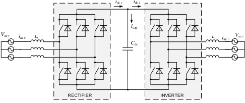
RECTIFIER INVERTER
iac r Lr
Vac r
idc r idc i
icap
Cdc
Li iac i
[image:1.612.51.294.489.591.2]Vac i
TPEL-Reg-2015-08-1401 - Final Edition
PWM interleaving has attracted an interest of researchers investigating harmonics reduction. The idea of this method is to cancel the harmonics by manipulating the PWM carrier waveforms. In [12] the effectiveness of this technique to minimize the harmonics of multilevel converters was demonstrated. The method was applied to reduce harmonic currents in the AC line for paralleled inverters [13]. The PWM interleaving concept has also been applied in DC-AC-DC converters [14] to reduce the DC-link ripple current by adjusting the carrier phases of DC-DC part according to the inverter input current. Nguyen [15] applies the method to space-vector PWM and uses two non-adjacent active vectors to reduce the DC-link capacitor ripple current from a three-phase inverter. Gui-Jia Su in [16] uses segmented inverters to drive an induction motor with parallel windings; it is found that the capacitor harmonic current can be significantly reduced by interleaving the carriers of each inverter by 180o. However, there have been no publications dealing with the minimization of switching harmonics in the two-level back-to-back AC-DC-AC topology using PWM carrier phase shifting. This method of current ripple cancelation is investigated in this paper.
II. THE PROPOSED APPROACH:OVERVIEW
For the considered converter the DC-link capacitor current is a superposition of the DC currents coming from the rectifier idcr
and the inverter idci. The phases of harmonics components in the
two currents, idcr and idci, are determined by the operating
conditions and by the relative phase PWM carriers of the rectifier and the inverter. Hence there is a potential to employ PWM interleaving techniques in order to reduce the DC-link capacitor harmonic current. In order to achieve this goal the following issues have to be considered:
1) As the fundamental frequencies and the carrier frequencies of the two converters are usually different, the frequencies of the harmonics generated into DC-link are different as well. It is therefore not usually possible to cancel the harmonics using a simple phase shift;
2) The minimized DC-link capacitor harmonic current can be obtained using the optimal PWM shift angle, with which the DC-link harmonic currents from rectifier and the inverter are in-phase. The optimal PWM carrier shift angle varies with the operation conditions and the converter hardware design in practice. It would therefore be difficult to apply a fixed PWM carrier shift angle in order to reduce the harmonic content, hence some active control over the carrier shift should be proposed.
This paper proposes the use of active solution to the cancellation as well as introducing a novel method of active DC-link capacitor harmonic current minimization. The active control adjusts both the frequencies and the phases of PWM carriers in the rectifier and the inverter such that the DC-link harmonic currents from the two converter stages are in phase. As a result the capacitor harmonic current can be minimized.
III. THE ANALYTICAL SOLUTION FOR THE DC-LINK
CAPACITOR HARMONIC CURRENT
To fully consider the compensation of the DC-link harmonic current the work of McGrath and Holmes [10] has to be extended to include the effect of individual PWM carriers phase shift on the components of the harmonic current.
Consider the back-to-back converter shown in Fig.1, in which both the rectifier and the inverter each have 3 phase legs. The DC-link harmonic current idc(t) generated by each phase leg can
be represented as the multiplication of the ac current iac(t)and
the switching function sf(t):
( )
( )
( )
dc ac
i t
sf t
i t
(1) Due to the switching behavior of the converters, there will be some harmonic currents on the AC sides as well. However, the amplitudes of these harmonics are usually very small and are not addressed in this work. The AC current can therefore be represented by just fundamental frequency component:
0
( ) cos(2 )
ac ac
i t I f t (2)
where Iac is the amplitude of fundamental component, β is the
angle between AC fundamental current and AC source voltage, and f0 is the fundamental frequency. Neglecting the DC bias, the
harmonic components of the switching function for a phase leg under sinusoidal asymmetrical regular sampled PWM can be derived [9]:
0,1 0 0
+
, 0 0
1
-( ) = cos(2 )
+ m ncos( [2 c c] [2 ])
m n
sf t K f t
K m f t n f t
(3)where
,
1
( ) sin([ ] )
2
m n n
K J qM m n
q
(4)
2 2
0 0
( 2 sin ) (2 cos )
/ 2
ac ac ac
dc
V f LI f LI
M
V
(5) Here, M is the PWM modulation depth, L is the line inductance,
Vac is the amplitude of ac side voltage source, Vdc is the DC-link
voltage, θ0 is the fundamental phase angle, fc is the PWM
carrier frequency, q=(m+nf0/fc)π/2, m is the carrier band
number and n is the side band number. Using (1-5), the DC-link harmonic currents generated by one phase leg can be obtained:
0,1 0 0 0
, 0 0
1 0 0
{cos(4 ) cos( )}
( ) {cos(2 [ ( 1) ] )
2
cos(2 [ ( 1) ] )}
ac
dc m n c c
m n c c
K f t
I
i t K mf n f t m n
mf n f t m n
(6)
where θc is the carrier phase angle. By analyzing (6) it can be
shown that the frequency distribution of the DC-link current harmonics is a superposition of switching function with frequency shifts of (n+1)f0 and (n–1)f0. It can also be shown that
the phase variance between the AC current and the DC-link current harmonics are coupled by the PWM modulation. The relative phases of DC currents harmonics can be varied by the shifting the carrier phase, θc, even if the frequencies of the DC
TPEL-Reg-2015-08-1401 - Final Edition
For both the rectifier and the inverter stages of the back-to-back converter the DC-link harmonic currents are a superposition of the harmonic currents from each phase leg. The difference between the rectifier and the inverter DC currents will determine the harmonic content of the ripple current through DC-link capacitor.
In a standard PWM scheme, all converter legs use the same carrier signal [10]. Assuming that each leg has an individual carrier waveform, the instant carrier phase angle θc in each leg
can be regarded as consisting of the reference carrier phase θcc
and the individual inter-leg phase angles θcp with respect to the
reference phase angle. These definitions are shown in Fig.2 where the reference θcc is set as a carrier angle of phase A.
Phase A is taken as the reference for the inter-leg carrier angles in both converters and the carrier phase angle of the inverter θci
is set to 0.
By using (3)-(6), the following equation for DC-link capacitor current in back-to-back converter can be derived:
0,1 0 ,1 ,1
2
0 ,
0 ,
1 0 ,
( ) ( ) ( )
cos(4 ) cos( )
cos(2 [ ( 1) ] )
2
cos(2 [ ( 1) ] )
2 cap dci dcr
r r r k r k
acr
cr r cprk cc r k n
k r m n
m n cr r cprk cc r k n
aci
i t i t i t
K f t
I
mf n f t m m K
mf n f t m m
K I
0,1 0 ,1 ,1
2
0 ,
0 ,
1 0 ,
cos(4 ) cos( )
cos(2 [ ( 1) ] ) cos(2 [ ( 1) ] )
i i i k i k
ci i cpik i k n
k i m n
m n ci i cpik i k n
f t
mf n f t m K
mf n f t m
(7) where , 2 2 3 3 k n k kn n
(8)
,
2 2
3 3
k n
k k
n n
(9) Here, α is the angle between ac fundamental current and ac-side converter voltage. k is the phase number: k = 0, 1 or 2 for phases A, B or C respectively.
From (7) it can be seen that both the frequencies and the phases of the DC-link harmonic current components can be manipulated by changing the carrier phases of the rectifier and the inverter. Based on this result, an active control method for DC-link capacitor harmonic current reduction can be proposed.
IV. THE PROPOSED HARMONIC CURRENT MINIMIZATION
METHOD
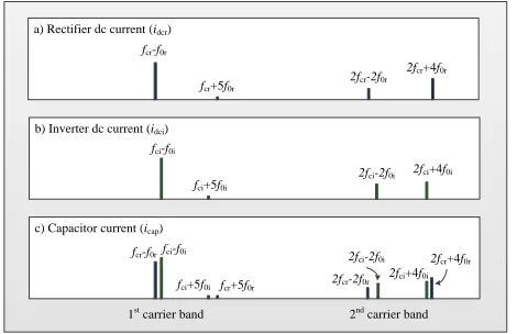
The DC-link current spectrum in a back-to-back converter under conventional sinusoidal asymmetrical regular sampling PWM is analyzed in [9] as shown in Fig.3. Both the rectifier and the inverter have two significant current harmonics in the 1st carrier band (at frequencies fc-3f0 and fc+3f0) and one
harmonic in the 2nd carrier band (at 2fc). The DC-link capacitor
harmonic current is the superposition of the harmonics seen in each converter stage.
By controlling the PWM carrier phase shift, the frequencies and the phases of the harmonic in the DC-link harmonic currents in the 1st carrier band can be substantially reduced.
The approach can be implemented in three steps:
1) Reduction of the number of significant harmonics in the 1st carrier band.
2) Adjusting the frequencies of the remaining harmonics from the rectifier and inverter in the 1st carrier band such that they become identical.
3) Synchronizing the phases of remaining harmonics in the 1st band to achieve their ultimate cancellation. These three steps are considered in detail below.
Step 1: Reducing the number of significant harmonics in the 1st
carrier band.
In this step the carriers of phases B and C are phase shifted by 2π/3 and -2π/3 respectively; a carrier phase shift of(0, 2π/3, -2π/3) is applied. The current harmonics in the 1st carrier band under such a phase shift can be derived from (6):
1 4 0
6 0
2 0
0 0
3
( ) { ( ) cos(2 [ 5 ] 4 ]) 2
( ) cos(2 [ 5 ] 6 ]) ( ) cos(2 [ ] 2 ]) ( ) cos(2 [ ] ])} ac
dc Shift c cc
c cc
c cc
c cc
I
i t J qM f f t q
J qM f f t J qM f f t J qM f f t
(10)
The harmonics in the 1st band have been shifted to frequencies (fc-f0) and (fc+5f0). Since the Bessel function Jx() is a decreasing
function of x, the amplitude of the harmonic at (fc+5f0) is much
fcr-3f0r
fcr+3f0r
2fcr
a) Rectifier dc current (idcr)
fci-3f0i
fci+3f0i
2fci
b) Inverter dc current (idci)
fcr-3f0r
fcr+3f0r 2fcr
c) Capacitor current (icap)
fci-3f0i
fci+3f0i 2fci
[image:3.612.47.285.266.488.2]1st carrier band 2nd carrier band
Fig. 3. Original DC-link current spectrum with conventional SPWM
θcpi1 θcpi2 θcpr2 θcpr1 θccr
inverter:
rectifier:
phase A phase B phase C phase B phase A phase C [image:3.612.328.550.281.424.2]TPEL-Reg-2015-08-1401 - Final Edition
less than the component at (fc-f0), therefore it can usually be
ignored. The number of significant harmonics in the 1st carrier band is therefore reduced to one as the result of this step. Similarly, the analytical solution for the 2nd carrier band under a carrier phase shift of (0, 2π/3, -2π/3) can be shown to be:
2 3 0
1 0
3 0
5 0
3
( ) { ( ) cos(2 [2 2 ] 2 3 ]) 2
( ) cos(2 [2 2 ] 2 ]) ( ) cos(2 [2 4 ] 2 3 ])
( ) cos(2 [2 4 ] 2 5 ])} ac
dc Shift c c
c c
c c
c c
I
i t J qM f f t q
J qM f f t J qM f f t J qM f f t
(11)
If the carrier shift is not applied then the current harmonics can be calculated from (6) by substituting the phase shift (0,0,0) into (6):
2 1
3
( ) ( ){cos(4 2 ) 2
cos(4 2 )}
ac
dc NoShift c c
c c
I
i t J qM f t
q f t (12)
Comparing (11) and (12), it can be seen that the current harmonics in the 2nd carrier band can also be reduced by applying the proposed method. The result of applying the proposed inter-leg carrier angle shift is shown in Fig.4. The DC-link capacitor current has only two significant harmonics in the 1st carrier band and the 2nd band includes four components, but of smaller magnitudes compare to the case with no carrier phase shift.
Step 2: Adjusting the frequencies of the harmonics in the 1st
carrier band.
In the second step, the frequencies of the remaining current harmonics in the 1st carrier band of the capacitor current are made identical. This can be achieved by adjusting the converters carrier frequencies according to the harmonic frequency, fh. Since the frequency of the main harmonic in the
1st band for each converter following Step 1 is fc-f0, the adapted
carrier frequency can be found using: 0
c h
f f f (13)
The resulting 1st-band current harmonics from both the inverter and rectifier converters will be at the same frequency fh, and the
lower-side harmonics of the 2nd band will also be at the same frequency, 2fh , as shown in Fig.5.
Step3: Synchronizing the 1st carrier band harmonics
In the final step the inverter’ and rectifier’ harmonics in the 1st
carrier band are synchronized so that they are in phase. Under this condition, the result of their superposition will be zero and the corresponding current harmonics in the DC-Link capacitor will disappear.
The analytical solution for the remaining harmonic in the 1st carrier band can be found:
1 0 r
2
0
2 3
( ) { ( ) cos(2 )
2
( ) cos(2 2 )}
3
{ ( ) cos(2 )
2
( ) cos(2 2 )}
acr
cap r r h cc r
r
r r h cc r r r
aci
i i h i i
i
i i h i i i
I
i t J q M f t
q
J q M f t
I
J q M f t
q
J q M f t
(14)
where, φ=4π∆fct+2θc0, ∆fc is the carrier frequency error and θc0
is the initial carrier angle. The phaseof the harmonic depends on the operation conditions of both converters (PWM modulation depth, current magnitude and power factor) and the relative initial carrier angles θc0r and θc0i if the rectifier and
inverter are controlled using different control platforms. The carrier frequency error ∆fc may also be generated by the
discretization of the digital control system and any output variance of the oscillators, both of which can introduce harmonic phase errors.
In order to keep the harmonics from the rectifier and the inverter in phase, closed-loop control of the harmonic phase difference is established by varying the carrier phase angle of one of the converter (in this study the rectifier was selected) according to:
cc i r
(15)where γ is the phase of the significant current harmonic in the 1st carrier band after the inter-leg carrier shift has been applied. The values of γr and γican be found from the DC-link currents
of each converter using band-pass filters. The current spectrum following this step is shown in Fig.6.
By comparing Fig. 3 with Fig. 6, it can been seen that the three-stage procedure leads to a significant reduction of harmonic content in the 1st and the 2nd carrier bands of DC-link capacitor current. Hence a DC-link capacitor of a much smaller
fcr-f0r
fcr+5f0r
2fcr+4f0r
a) Rectifier dc current (idcr)
fci-f0i
fci+5f0i
b) Inverter dc current (idci)
fcr-f0r
fcr+5f0r
c) Capacitor current (icap)
fci-f0i
fci+5f0i
1st
carrier band 2nd
carrier band
2fcr-2f0r
2fci+4f0i
2fci-2f0i
2fcr+4f0r
2fcr-2f0r 2fci+4f0i
[image:4.612.321.554.130.279.2]2fci-2f0i
Fig. 4. DC-link current spectrum following Step 1.
fcr-f0r
fcr+5f0r
2fcr+4f0r
a) Rectifier dc current (idcr)
fci-f0i
fci+5f0i
b) Inverter dc current (idci)
fcr+5f0r
c) Capacitor current (icap)
fci+5f0i
1st
carrier band 2nd
carrier band
2fcr-2f0r
2fci+4f0i
2fci-2f0i
2fcr+4f0r
2fci+4f0i
Superposition of harmonics
[image:4.612.59.294.355.507.2]at fh ( fh = fci-f0i = fcr-f0r) Superposition of harmonics at 2f h (2fh=2fci-2f0i=2fcr-2f0r)
TPEL-Reg-2015-08-1401 - Final Edition
size can be used to meet the power quality specifications and the capacitor losses will be reduced.
V. EXPERIMENTAL VERIFICATION
The experimental verification of the proposed method was conducted using a two-level back-to-back converter based test rig with the control structure as shown in Fig. 7. The test rig basic parameters are given in Table I.
A large DC-link capacitor is used to smooth the DC-link voltage; therefore the impact of voltage ripple on switching harmonic current can be neglected. Two Infinite Impulse Response (IIR) band-pass filters are implemented using Field Programmable Gate Arrays (FPGA) to extract the current harmonics of the 1st carrier band, as discussed in previous Section. The PWM generator are also implemented to generate required carrier-shifted PWM. The rectifier carrier angle θcc is
derived by calculating the harmonic phase difference and updated every 1/3rd second. The ac voltage fundamental frequency in both converters is measured by Phase Lock Loops (PLL) [18].
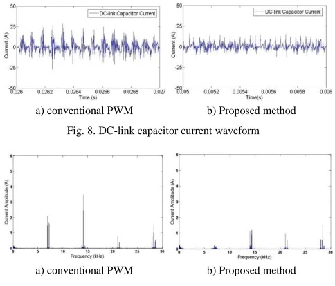
A comparison of the DC-link currents for operation under conventional PWM and under PWM with the proposed control method is shown in Fig.8 and Fig.9. For both cases the operation point was defined by inverter ac-side current Iaci =
7.8A and β = 23°.
The magnitude of the DC-link capacitor current ripple reduces when the proposed control method is applied, as shown in Fig 8. The harmonic reduction is clearly seen from DC-link current spectrums shown in Fig.9. Comparing results obtained
without and with the proposed method, it is clear that the Total Harmonic Distortion of the DC-link capacitor current, which is calculated against the DC component of DC-link current, is greatly reduced from 154% to 46% when the proposed control method is applied to the converter in this example.
VI. APPLICATION CONSIDERATIONS
This Section considers some practical issues related to the application of the proposed carrier shift method under different converter operating scenarios.
A. Dynamic response of the phase synchronization
The proposed control method relies on keeping the significant harmonic currents in the 1st carrier band in phase. Under dynamic operating conditions this is achieved by updating the converter carrier angle. For example, the response of harmonics phase difference γi- γr and the power factor of the inverter to the
step change of AC current amplitude are shown in Fig.10(a) and (b) respectively. If the inverter power factor is maintained
fcr-f0r
fcr+5f0r
2fcr+4f0r
a) Rectifier dc current (idcr)
fci-f0i
fci+5f0i
b) Inverter dc current (idci)
fcr+5f0r
c) Capacitor current (icap)
fci+5f0i
1st
carrier band 2nd
carrier band
2fcr-2f0r
2fci+4f0i
2fci-2f0i
2fcr+4f0r
2fci+4f0i
Superposition of harmonics at fh ( fh = fci-f0i = fcr-f0r)
[image:5.612.314.567.62.224.2]Superposition of harmonics at 2fh (2fh=2fci-2f0i=2fcr-2f0r)
Fig. 6. DC-link current spectrum as a result of Step 3.
Fig. 7. Test rig control for the experimental verification
TABLE I.TEST RIG PARAMETERS
Parameters Value
DC-link capacitance. mF 4.4
Rectifier line inductance Lr. mH 2.33
Inverter line inductance Li, mH 2.33
DC bus voltage, V 750
Rectifier power factor Unity
Power supply voltage, Vrms 240
Output Power supply frequency, Hz 60
Grid voltage, Vrms 240
Grid frequency, Hz 50
Predefined significant harmonic frequency fh in the
1st carrier band, Hz 7000
Bandwidth of IIR band-pass filter, Hz 6900-7100
[image:5.612.55.291.79.230.2]a) conventional PWM b) Proposed method
Fig. 8. DC-link capacitor current waveform
[image:5.612.320.562.290.497.2]a) conventional PWM b) Proposed method
[image:5.612.54.295.346.509.2]TPEL-Reg-2015-08-1401 - Final Edition
at 0.92 and the AC inverter current demand steps from 3.9A to 7.8A then the harmonic phase difference returns to zero with a minor overshoot, as shown in Fig.10(a).
The carrier phase angle updates every 0.33 seconds and following the disturbance the harmonic resynchronization
occurs within one cycle. A faster response can be achieved if a smaller update interval is used.
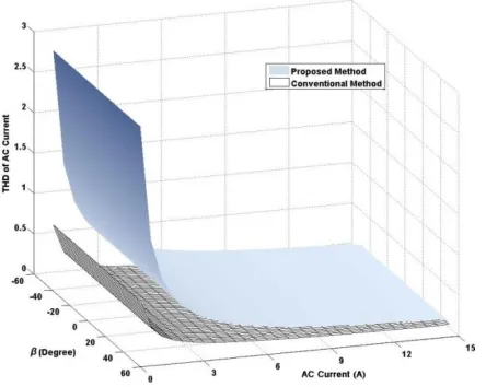
B. Effect of difference in harmonic magnitudes
The magnitudes of the DC-side harmonics in the 1st carrier band from each converter may become unequal as a result of changes in operating conditions or converter parameters fluctuations. In this case, some residual harmonics will be observed in the 1st carrier band as they will not fully cancel. In order to assess the effect of this difference, the Total Harmonic Distortion (THD) was calculated as (16). In is the RMS value of
DC harmonic current, the fundamental frequency for this case is 10Hz, IDC is the DC component of DC-link current.
2 2 2 2
1 2 n1 n DC
I I I I
THD
I
(16)
Based on the analytical solution of harmonics in (7), the THDs are evaluated for different combination of Iaci and βi of inverter
when the rectifier operates with unity power factor (βr=0). The
THD results over the Iaci and βi plane is shown in Fig.11. As can
be seen, the proposed method leads to a lower THD comparing with the conventional PWM THD if β<45° and the minimum THD is observed if β≈23°. The THD is strongly influenced by the difference in the 1st-band harmonic magnitudes of each converter. The latter, according to analytical results shown in Section III, are defined by values of q and M. In this example, the inverter’s q is larger than the rectifier’s q, hence the inverter’s harmonic magnitude and the modulation depth M are larger than those of the rectifier when β is zero. As β increases, the inverter’s harmonic magnitude decreases and hence the THD decrease. Beyond this point (β≈23°), the inverter’s harmonic magnitude is smaller than that of the rectifier, therefore full cancellation does not occur and the THD increases. For a fixed value of β, both the DC-link current component and its harmonics increase proportionally to the AC
current, therefore the THD varies little with the ac current, as shown in Fig.11.
C. Effect on the common-mode voltage
The proposed carrier shift control does not only impact on the harmonics seen in the DC-link current, it also influences the common mode voltage.
Due to the inter-leg carrier shift the zero vectors are represented by two reverse active vectors with the same duration. In a typical PWM output waveform within one duty cycle as shown in Fig.12 the zero voltage vectors are represented by two opposite active vectors V3 and V6; such a PWM pattern is
known to help reduce the common mode voltage [15].
The common-mode voltage measured between the neural of the delta-wye transformer and the earth is shown in Fig.13. It can be seen that the peak value of the common-mode voltage is substantially reduced when the proposed control method is applied.
a) conventional PWM b) Proposed method
Fig.12. Effect of inter-leg carrier phase shift on the PWM pattern
a) conventional PWM b) Proposed method
Fig.13. Comparison of common-mode voltages
D. Effect on AC-side current harmonics
The rectifier’s AC-side current harmonic spectrum with and without the proposed method are shown in Fig.14. It can be
Fig.10. Harmonics phase difference in response to change in operation conditions (Inverter power factor is fixed at 0.92, and the ac current
amplitude steps from 3.9A to 7.8A)
TPEL-Reg-2015-08-1401 - Final Edition
[image:7.612.47.299.83.162.2]seen that the proposed carrier shift increases the 1st carrier band harmonics in the AC-side current.
Fig.14. Comparison of AC current harmonic spectrum for rectifier
In conventional PWM there are two significant harmonic currents at fc+2f0 and fc-2f0, both with similar amplitudes. The
application of the carrier shift eliminates the harmonic at fc+2f0
but introduces a new harmonic at frequency fc. This harmonic is
approximately twice the magnitude of the harmonic at fc+2f0
for the conventional PWM case. The THD value of ac current as a function of Iac and β was assessed and illustrated by Fig.15.
The THD of the ac current under the proposed control method is slightly worse compare to the THD of the conventional PWM, especially for small ac current values. This effect is due to the asymmetry of active vector placement in a PWM cycle, as shown in Fig.12.
VII. CONCLUSIONS
A novel method of active minimization of current waveform harmonics in the DC-link capacitor of a two-level back-to-back converter has been proposed. The method is based on a derived analytical solution for the DC-link harmonic current which shows that by adjusting the frequencies and phases of PWM carriers of rectifier and inverter the harmonic content in the 1st and the 2nd carrier bands can be significantly reduced. The proposed method can be implemented in three steps and the approach has been experimentally validated.
The proposed method will be of practical interest for applications of back-to-back converters in which a critical design parameter is the mass and volume of DC-link capacitors, for example in automotive and aerospace applications.
REFERENCES
[1] Bon-Gwan Gu; Kwanghee Nam, "A DC-link capacitor minimization method through direct capacitor current control," Industry Applications, IEEE Transactions on , vol.42, no.2, pp.573-581, March-April 2006 [2] Pena, R.; Clare, J.C.; Asher, G.M., "Doubly fed induction generator
using back-to-back PWM converters and its application to variable-speed wind-energy generation," Electric Power Applications, IEE Proceedings - , vol.143, no.3, pp.231-241, May 1996
[3] Areerak, K-N.; Bozhko, S.V.; Asher, G.M.; De Lillo, L.; Thomas, D.W.P., "Stability Study for a Hybrid AC-DC More-Electric Aircraft Power System," Aerospace and Electronic Systems, IEEE Transactions on , vol.48, no.1, pp.329-347, Jan. 2012
[4] Maheshwari, R.; Munk-Nielsen, S.; Kaiyuan Lu, "An Active Damping Technique for Small DC-link Capacitor Based Drive System," Industrial Informatics, IEEE Transactions on , vol.9, no.2, pp.848-858, May 2013 [5] Wook-Jin Lee; Seung-Ki Sul, "DC-link Voltage Stabilization for
Reduced DC-link Capacitor Inverter," Industry Applications, IEEE Transactions on , vol.50, no.1, pp.404-414, Jan.-Feb. 2014
[6] Jinhwan Jung; Sunkyoung Lim; Kwanghee Nam, "A feedback
linearizing control scheme for a PWM converter-inverter having a very small DC-link capacitor," Industry Applications, IEEE Transactions on , vol.35, no.5, pp.1124-1131, Sep/Oct 1999
[7] Deslauriers, I.; Avdiu, N.; Ooi, B.T., "Naturally sampled triangle carrier PWM bandwidth limit and output spectrum," Power Electronics, IEEE Transactions on , vol.20, no.1, pp.100,106, Jan. 2005.
[8] Winkelnkemper, M.; Bernet, S., "Impact of control model deviations on the DC link capacitor minimization in AC-DC-AC converters," Industrial Electronics Society, 2005. IECON 2005. 31st Annual Conference of IEEE , vol., no., pp.6 pp.,, 6-6 Nov. 2005
[9] Kolar, Johannw Walter and Round, Simon D., “Analytical calculation of the RMS current stress on the DC-link capacitor of voltage-PWM converter systems,” Electric Power Applications, IEE Proceedings -, vol. 153, no. 4, pp. 535-543, August. 2001.
[10] McGrath, B.P.; Holmes, D.G., "A General Analytical Method for Calculating Inverter DC-link Current Harmonics," Industry Applications, IEEE Transactions on , vol.45, no.5, pp.1851-1859, Sept.-oct. 2009.
[11] Kieferndorf, F.D.; Forster, M.; Lipo, T.A, "Reduction of DC-bus capacitor ripple current with PAM/PWM converter," Industry Applications, IEEE Transactions on , vol.40, no.2, pp.607,614, March-April 2004.
[12] McGrath, B.P.; Holmes, D.G., "Multicarrier PWM strategies for multilevel inverters," Industrial Electronics, IEEE Transactions on , vol.49, no.4, pp.858-867, Aug 2002.
[13] Di Zhang; Wang, F.; Burgos, R.; Rixin Lai; Boroyevich, D., "Impact of Interleaving on AC Passive Components of Paralleled Three-Phase Voltage-Source Converters," Industry Applications, IEEE Transactions on , vol.46, no.3, pp.1042-1054, May-june 2010.
[14] Xi Lu; Wei Qian; Dong Cao; Fang Zheng Peng; Jianfeng Liu, "A carrier modulation method for minimizing the dc link capacitor current ripple of the HEV DC-DC converter and inverter systems," Applied Power Electronics Conference and Exposition (APEC), 2011 Twenty-Sixth Annual IEEE , vol., no., pp.800-807, 6-11 March 2011
[15] The Dung Nguyen; Patin, N.; Friedrich, G., "Extended Double Carrier PWM Strategy Dedicated to RMS Current Reduction in DC Link Capacitors of Three-Phase Inverters," Power Electronics, IEEE Transactions on , vol.29, no.1, pp.396-406, Jan. 2014.
[16] Gui-Jia Su; Lixin Tang, "A segmented traction drive system with a small dc bus capacitor," in Energy Conversion Congress and Exposition (ECCE), 2012 IEEE , vol., no., pp.2847-2853, 15-20 Sept. 2012 [17] Cacciato, M.; Consoli, A; Scarcella, G.; Testa, A, "Reduction of
common-mode currents in PWM inverter motor drives," Industry Applications, IEEE Transactions on , vol.35, no.2, pp.469-476, Mar/Apr 1999.
[18] Kaura, V.; Blasko, V., "Operation of a phase locked loop system under distorted utility conditions," Industry Applications, IEEE Transactions on , vol.33, no.1, pp.58-63, Jan/Feb 1997.
[19] DO-160E Environmental Conditions and Test Procedures for Airborne Equipment, RTCA standard, 2004.
a) conventional PWM b) Proposed method
[image:7.612.64.286.337.514.2]TPEL-Reg-2015-08-1401 - Final Edition
[20] MIL-STD-704 Aircraft Electrical Power Characteristics, United States Military Standard, 2004.
ACKNOWLEDGMENT