1
The authors are with the Department of Electrical and ElectronicEngineering, The University of Nottingham, University Park, Nottingham NG7 2RD, United Kingdom (Jianfeng.Li@ nottingham.ac.uk, [email protected], dai.t. [email protected], [email protected], eexakso @nottingham.ac.uk, Mark.Johnson@ nottingham.ac.uk).
Built-in reliability design of highly integrated solid-state
power switches with metal bump interconnects
Jianfeng Li, Alberto Castellazzi, Member,
IEEE
, Tianxiang Dai, Martin Corfield, Adane
Solomon, Christopher Mark Johnson, Member,
IEEE
Abstract A stacked substrate-chip-bump-chip-substrate assembly has been demonstrated in the construction of power switch modules with high power density and good electrical performance. In the present work, special effort has been devoted to material selection and geometric shape of the bumps in the design for improving the thermo-mechanical reliability of a highly integrated bi-directional switch. Results from Three-dimensional finite element simulation indicate that for all design cases the maximum von Mises stresses and creep strain accumulations occur in the solder joints used to join bumps on IGBTs during a realistic mission profile, but occur in the solder joints used to join bumps on DBC substrates during accelerated thermal cycling. The results from both the simulation and the accelerated thermal cycling experiments reveal that selection of Cu/Mo/Cu composite brick bumps in the stacked assembly can significantly improve the thermo-mechanical reliability of both the solder joints and the DBC substrates when compared to Cu cylinder bumps and Cu hollow cylinder bumps reported in previous work. Such results can be attributed to the effective reduction in the extent of mismatch of coefficients of thermal expansion between the different components in the assembly.
.
Index Terms Integration, wire-less packaging, Cu/Mo/Cu composite, finite element method, thermal cycling.
I. INTRODUCTION
Wire-bond interconnect technology is the standard method that has widely been used to achieve the electrical interconnects on the front side of power devices in power modules. However, wire bonds have limited ability to dissipate heat and have relatively high parasitic inductance which often restricts the thermal and electrical performance of the power modules. To overcome this problem, several replacements of wire-bonds, such as ribbon-bond [1], dimple array [2], embedded chip technology [3]-[5], silicon interposer [6], solder bump [7], metal bump [8]-[12] and press-pack bus-bar-like interconnects [13] have been proposed and investigated over the past years. Of them, metal bump interconnects, also called solid interconnect posts, have been
demonstrated not only to obtain dramatic improvement in the thermal and electromagnetic performance, but also allow advanced integration schemes, e.g. stacked devices, for the optimization of basic power switch topologies, e.g. half bridge switch and bi-directional switch [14]-[16]. However, further investigation of reliability and manufacturability for the implementation of this technology is still needed for wider acceptance and generalization.
Metal bumps (or posts) may be formed using double etching and electro-plating and joined using bonding technology [8]-[12]. Haque et al. [8] used Cu brick posts and soldering technology to develop a metal posts interconnected parallel structure power module. Their results demonstrated the improved electrical performance of the developed power module when compared to corresponding Al wire bonded power modules. Johnson et al. [9] created Cu posts on direct bond copper substrates using a double etching process. The posts were created to make contact on the top side of power devices for assembling a sandwich structure power module with low parasitic inductances. Zeanh et al. [10] investigated the thermo-mechanical reliability of an insulated gate bipolar transistor (IGBT) module constructed with Cu cylinder bumps and soldering technology, and identified the solder joints used to bond the bumps as thermo-mechanically weak points. Menager et al. [11] deposited brick-like Cu micro-posts on the top sides of power diodes, and achieved good electrical connection for a 3D packaging of power modules. Lee et al. [12] prepared deposited cylindrical Cu bumps and micro-stud structure on Si wafers for Cu-Cu 3D packaging, and then used electroless Ni plating to compensate for the bump height variation. Solomon et al. [14]-[16] used Cu brick and Cu hollow cylinder bumps to develop highly integrated bi-directional switch and half bridge switch modules, and obtained dramatic improvements in the thermal and electromagnetic performance.
2
However, the solder joints for bonding the bumps on theIGBTs are the thermo-mechanical weak points with the maximum creep strain accumulation. The combination of Si3N4-based substrates with hollow cylinder bumps can slightly reduce the creep strain accumulation in the critical solder joints when compared to the other combinations of Al2O3 and AlN-based substrates with both the solid and hollow cylinder bumps.
This paper presents an extended and more comprehensive FE modelling approach to optimize the thermo-mechanical performance of the stacked bi-directional power switch assembly. First, both pure Cu and Cu/Mo composite were selected as the bump materials, with brick, cylinder and hollow cylinder (with different wall thickness) for the geometric bump shapes. Then three-dimensional FE modelling will be used to simulate and compare the thermo-mechanical response of the stacked assemblies designed using the different bumps under not only a mission profile but also an accelerated thermal cycling test between -55 ºC and +150 ºC. In addition, the FE simulation results will be evaluated against the accelerated thermal cycling test from two stacked assembly samples constructed with hollow cylinder Cu bumps and brick Cu/Mo/Cu composite bumps.
The main objectives of this paper are: (i) to summarize the FE simulation results which may be used for optimization of the thermo-mechanical performance of power modules; (ii) to compare the different thermo-mechanical response of the stacked assemblies under the mission profile and accelerated thermal cycling tests; (iii) to demonstrate the equivalent importance of both geometric bump shape and selection of material for achieving improved thermo-mechanical reliability of stacked assemblies; and (iv) to evaluate the FE simulation
results with those of the thermal cycling experiments.
II. DESIGN CONSIDERATION
A. Overall design
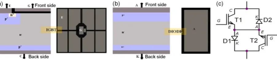
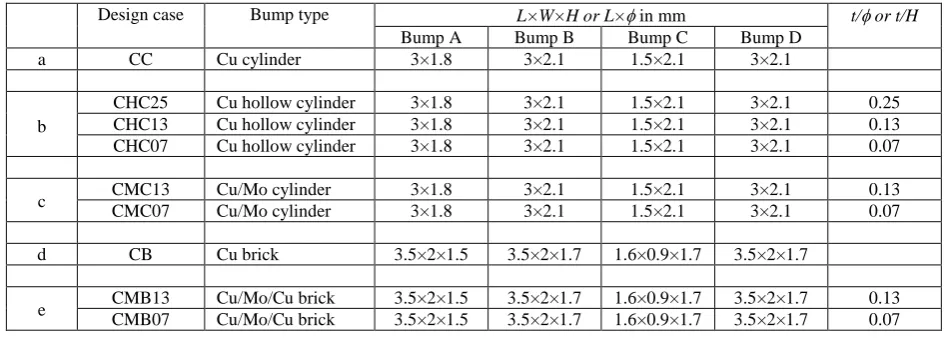
As reported in the previous preliminary study [17], the stacked assembly of substrate-chip-bump-chip-substrate has been designed for implementing a bi-directional switch constructed with 70 m thin IGBTs and diodes, rated at 200A-600V, as shown in Fig. 1, in which their front metallization has been treated with a NiP/Pd finish to aid solderability. The footprint of one IGBT is 109.50.07 mm, and that of one diode is 9.55.50.07 mm. In the designed assembly as shown in Fig. 2, the front side (with conductor circuit tracks) of both the top and bottom substrates are used for attaching one IGBT and one diode and provide terminals for gate and emitter contact for the IGBT attached on the opposite substrate. With this assembly the backside of both substrates can function as primary cooling surfaces for achieving double-sided cooling. AlN-based substrates are selected for both the top and bottom substrates, which consist of 0.3 mm thick direct bonded Cu (DBC) on 1 mm thick AlN ceramic tiles. The bumps A (as shown in Fig. 2) are used to provide the electrical interconnects between the IGBTs and the opposite diodes. The bumps B are used to provide the electrical interconnects between the IGBTs and the opposite substrates. The bumps C are used to connect the gate signals of the IGBTs from the opposite substrates. In addition, the bumps D are used to achieve all inputs, outputs and signals of the switch to be terminated on one substrate, and provide additional mechanical support to the assembly.
[image:2.595.83.535.452.551.2]
Fig. 1. Photographs of the 70um thin: (a) IGBT and (b) Diode chips; and (c) the schematic of the bi-directional power switch designed with two IGBTs and two diodes.
Fig. 2. The stacked assembly of substrate-chip-bump-chip-substrate for the bi-directional switch: (a) open view of the assembly with Cu/Mo/Cu composite brick; (b) top view of part of the assembly showing the layout of bumps A, B, C and D; and (c) closed view showing one entire assembly.
[image:2.595.69.534.589.712.2]3
thermal performance when compared to Si3N4 and Al2O3–based substrates in a stacked assembly under the same mission profile [17]. For example, provided that other conditions are identical, the highest maximum temperature in the assembly during the mission profile for 1 mm thick AlN ceramic tiles (used in DBC substrates) are approximately 12 C and 22 C lower than those for 0.3 mm thick Si3N4 ceramic tiles and 0.4 mm thick Al2O3 ceramic tiles, respectively. Furthermore, as presented below, two soldering steps have been used to assemble the present samples. 1 mm thick AlN tiles used in the substrates can reduce the bending deformation of the substrates down to lower than 20 µm after the first soldering step, while 0.3 mm thick Si3N4 ceramic tiles and 0.4 mm thick Al2O3 ceramic tiles used in the substrates lead to corresponding bending deformation higher than 100 µm. Therefore, AlN-based substrates are more suitable for manufacturing the designed switch module, and are hence selected for both the top and bottom substrates.
C. Bump shapes and selection of materials
Five types of bumps consisting of pure Cu or Cu/Mo
composite as shown in Fig. 3 have been considered to investigate the effects of bump shapes and selection of materials on the thermal performance and the thermo-mechanical reliability of the stacked assemblies. In Fig. 3, L is length, W is width, H is height, is diameter and t is thickness. Furthermore, several ratios of t to or t to H for the Cu hollow cylinder bump, the Cu/Mo shell/core composite cylinder bump and the Cu/Mo/Cu composite brick bump have also been taken into account. The dimensions of the bumps A, B, C and D shown in Fig. 2 for all the considerations of bump shapes and selection of materials are listed in Table I. For each of the design cases listed in Table I, the ratio of t to or t to H for all bumps A, B, C and D has remained a constant. These dimensions have been selected to ensure both sufficient insulating distance between the electrodes of the IGBTs and diodes in the assemblies and relative convenience for manufacturing. For example, commercially available or custom prepared Cu rods, tubes and plates can be used to cut or machine into Cu cylinders, Cu hollow cylinders and Cu
Fig. 3. Three-dimensional schematic diagrams of the 5 types of bumps considered in the present work: (a) Cu cylinder bump; (b) Cu hollow cylinder bump; (c) Cu/Mo shell/core composite cylinder bump; (d) Cu brick bump; and (e) Cu/Mo/Cu composite brick bump.
TABLEE I
THE TYPES, DIMENSIONS AND THE CORRESPONDING CODES FOR THE BUMP SHAPES AND SELECTION OF MATERIALS CONSIDERED IN THE DESIGN OF THE STACKED SUBSTRATE-CHIP-BUMP-CHIP-SUBSTRATE ASSEMBLY
Design case Bump type L×W×H or L× in mm t/ or t/H
Bump A Bump B Bump C Bump D
a CC Cu cylinder 3×1.8 3×2.1 1.5×2.1 3×2.1
b
CHC25 Cu hollow cylinder 3×1.8 3×2.1 1.5×2.1 3×2.1 0.25
CHC13 Cu hollow cylinder 3×1.8 3×2.1 1.5×2.1 3×2.1 0.13
CHC07 Cu hollow cylinder 3×1.8 3×2.1 1.5×2.1 3×2.1 0.07
c CMC13 Cu/Mo cylinder 3×1.8 3×2.1 1.5×2.1 3×2.1 0.13
CMC07 Cu/Mo cylinder 3×1.8 3×2.1 1.5×2.1 3×2.1 0.07
d CB Cu brick 3.5×2×1.5 3.5×2×1.7 1.6×0.9×1.7 3.5×2×1.7
[image:3.595.62.536.597.766.2]4
brick bumps, respectively. The shell/core Cu/Mo rods can beformed using metal wire drawing technology, and then cut into Cu/Mo composite cylinder bumps. The Cu/Mo/Cu plates can be produced using combined rolling and diffusion bonding process, and then stamped into the Cu/Mo/Cu composite brick bumps.
D. Solder joints
All the IGBT and diode attachments and bump interconnects are made with Sn-3.5Ag solder joints, and therefore eliminate the need for standard wire bond packaging technology. For attaching the IGBTs and diodes on the substrates, the Sn-3.5Ag solder joints have been designed to be 0.1 mm in thickness. For joining the bumps to the chips and/or to the substrates, the Sn-3.5Ag solder joints follow the shapes of the bumps, with a minimum thickness of 0.1 mm. It should be pointed out that the shapes of the solder joints shown in Fig. 2 are ideal approximations for subsequent FE modelling and simulation, and those of the actually reflowed solder joints may vary somewhat.
E. Assembling process
With automatic machines and/or suitable jigs for positioning the devices and bumps, the stacked substrate-chip-bump-chip-substrate assembly may be assembled using a single soldering step. In the present work, the samples for the thermal cycling test have been manually prepared using two soldering steps, where eutectic Sn-3.5Ag solder paste has been used in both steps. In the first soldering step, after applying solder paste on both substrates using stencil printing, one IGBT, one diode, two bumps B and all bumps D are placed on the bottom DBC substrate, and one IGBT and one diode placed on the top DBC substrate. Next, (after dispensing solder paste on one end of bumps A and C) two bumps of A and one bump of C are placed on the bond pads of the IGBT already placed on the bottom DBC substrate, and two bumps of A and one bump of C on the bond pads of the IGBT already placed on the top DBC substrate. Then, the bottom and top substrates (both with devices, bumps and solder paste) are placed into a reflow oven for soldering. Reflow soldering was accomplished using a temperature profile consisting of first heating up to 200 ºC within 3 min, holding at 200 ºC for 3 min, heating up to 250 ºC within 2 min, holding at 250 ºC for 3 min before being cooled down to room temperature within 6 min. In the second soldering step, solder paste was first applied to the other end of all the bumps already soldered on the substrates and the IGBTs. The top substrate was then placed and aligned on the bottom substrate through the use of an alignment jig. Finally, the whole assembly was placed in the reflow oven to finish the second soldering step, using a reflowing temperature profile identical to that used in the first soldering step.
III. THERMO-MECHANICL MODELLING
A. Meshing system
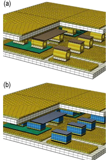
The thermo-mechanical modelling and simulation has been done using commercial available finite element analysis software Abaqus 6.11-3 and its graphic user interface CAE. Fig. 4 presents two representative meshing systems consisting of 162440 and 156294 elements (C3D8 linear brick elements
and DC3D6 linear triangular prism elements) to discretize the design cases CHC25 and CMB13. In both cases, the largest element is 1 1 0.45 mm, and the smallest element is 0.5 0.250.025 mm. In all the design cases listed in Table I, the elements used in the critical domains all have the same dimensions. For example, the sizes of the brick elements used to discretize the critical solder joints whose maximum von Mises stress and creep strain accumulation will be used to assess the thermo-mechanical reliability are all 0.5 0.250.025 mm in size. This is necessary because longer computing times would be required if meshing size-independent solutions were implemented for the present three-dimensional model with a much finer meshing system used. Therefore, relatively coarse meshing systems with the same size of elements (in the critical domains for all the design cases) have been employed to achieve an acceptable computing time.
[image:4.595.327.532.293.602.2]Fig. 4. Cut views of two representative meshing systems to discretize the stacked assembly for: (a) design case CHC25; and (b) design case CMB 13.
5
assumed as a layer of 3.2 µm thick Al on the top side and alayer of 1 µm thick Al on the back side of the chips in the present model. This is justified and based on the fact that most of the NiP/Pd and Ni/Ag layers react with liquid Sn-3.5Ag solder to form intermetallic compounds (IMCs) embedded within the matrix of the solder during the reflow process, and as such (the IMCs) have been neglected.
It should be pointed out that a more accurate three-dimensional model for analysing the thermo-mechanical performance of the stacked assembly should include the IMCs formed at the solder/contact metallization interfaces and their subsequent evolution during any thermal history. However, it is still a formidable task to solve such a three-dimensional thermo-mechanical problem because the IMCs are extremely thin when compared to other materials and parts in the model, and would require extremely fine elements to discretize them. Therefore, the formation and growth of the IMCs in this model have been ignored.
B. Thermal history and boundary conditions
The assembly was first subjected to a predefined temperature profile to simulate the stress and strain developments during the two-step reflow soldering process. During both soldering steps, the corresponding solder joints were deactivated without the development of stress and strain when they were in the form of either solder paste or molten solder. They were activated when they solidified from the molten solder. Both the solder paste and the solid solder joints are molten at the melting point of 221 ºC, and the solidification of the molten solder occurs at a super-cooling temperature of 192 ºC for Sn-3.5Ag solder alloys [18].
Fig. 5. Thermal history of predefined temperature profile of the two soldering steps followed by 5 cycles of mission profiles with heat generated by power losses of IGBTs and diodes.
Then the thermo-mechanical response of the assembly associated with 5 cycles of a realistic mission profile and 5 cycles of thermal cycling between -55 ºC and +150 ºC, as shown in Figs. 5 and 6, were further simulated independently. In the mission profile, the power losses of the IGBTs and diodes were taken as uniform surface heating sources. This may be somewhat different from the actual distribution of heating source in the devices [19], but can offer a relatively simple way to assess the thermal performance of the different design cases as listed in Table I. The heat exchange boundary
condition as described in Fig. 7 were applied to both the top and bottom cooling surfaces of the assembly, where the heat exchange coefficient of 5000 Wm-2k-1 is typical for a water-based cooler in power electronics [20]. The temperature field obtained from the thermal simulation was used as inputs to simulate further stress and strain development in the assembly during the mission profile. For the thermal cycling, a predefined uniform temperature field in the entire assembly (following the temperature profile) was directly applied to simulate further stress and strain developments. Thermal cycling between -55 ºC and +150 ºC has been selected because the reliability of the assembly samples for the design cases CHC25 and CMB13 had been experimentally tested under this thermal cycling condition.
Fig. 6. Thermal history of predefined temperature profile of the two soldering steps followed by 5 thermal cycles between -55 ºC and 150 ºC.
Fig. 7. Boundary condition of heat exchange applied in the thermal simulation during the mission profile.
[image:5.595.308.547.243.412.2] [image:5.595.45.283.426.594.2] [image:5.595.305.532.462.542.2]6
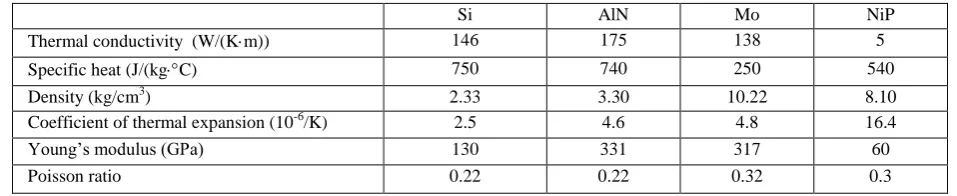
C. Properties of materialsThe thermal and mechanical properties of the Si, AlN ceramic, Mo and the NiP finish on the substrates for the thermo-mechanical simulation are listed in Table II [10], [21], and [22]. For the rest of the materials in the assembly, Chaboche’s plastic model was used to describe the mechanical properties of the Cu and Al, and Anand’s creep model was used to describe the mechanical property of the Sn-3.5Ag solder alloy. All the mechanical and thermal properties for the Cu, Al and Sn-3.5Ag were taken from Refs. [10], [21] and are therefore not repeated here.
In real applications, the stacked assembly will be filled
[image:6.595.66.545.256.354.2]with a soft dielectric encapsulant and integrated with a double-sided water-based cooler. These have been ignored because silicone gel, which is commonly used as the encapsulating gel, has extremely low thermal conductivity and Young’s modulus compared to the other components and parts in the assembly. Also using the backsides of the two DBC substrates as the primary cooling surfaces the mechanical constraint caused by installation of the double-sided water-based cooler will be limited. Therefore, the effect of ignoring the encapsulant and water-based cooler on the simulation results to be used for the optimization of the thermo-mechanical design should be negligible.
TABLE II
THERMAL AND MECHANICAL PROPERTIES OF PART OF THE COMPONENT MATERIALS USED DURING THE THERMO-MECHANICAL SIMULATIONS
Si AlN Mo NiP
Thermal conductivity (W/(Km)) 146 175 138 5
Specific heat (J/(kgC) 750 740 250 540
Density (kg/cm3) 2.33 3.30 10.22 8.10
Coefficient of thermal expansion (10-6/K) 2.5 4.6 4.8 16.4
Young’s modulus (GPa) 130 331 317 60
Poisson ratio 0.22 0.22 0.32 0.3
D. Simulation criteria for thermo-mechanical performance The effects of the bump shapes and materials on the maximum juncture temperature in the Si chips and on the thermo-mechanical reliability of the Sn-3.5Ag solder joints and DBC substrates have been considered. Regarding the possibility of thermo-mechanical failure of the solder joints, the maximum creep strain accumulation is adopted for qualitative comparison with the simulated creep strain fields for the different design cases [10], [23]-[26]. Thermo-mechanical failure of the DBC substrates is closely associated with the plastic strain development in the Cu metallization [27], [28]. However, brittle cracking of the AlN tiles is the dominant failure mode and is mainly controlled by tensile stresses [10], [21], [29], [30]. Thus, the maximum tensile principal stress is employed for qualitative comparison with the simulated stress fields for the different design cases.
It should be noted that these criteria are only regarded as indicators of the sequence and location of possible crack initiation, and are viewed as sufficient to provide insight and guidance for subsequent thermo-mechanical design and optimization. A more accurate prediction of the thermo-mechanical lifetime of the assembly would require a finer numerical model and a full description of the stress-strain behaviour and response of all the materials in the assembly under the relevant thermal history.
E. Simulation cases
All the 9 design cases listed in Table I have been simulated using the full model and subjected to the two types of thermal history associated with the mission profile and thermal cycling (as shown in Figs. 5 and 6). The design cases CHC25 and CMB13 have also been simulated using the simple model and subjected to the thermal history associated with the mission profile. In total 20 simulation cases have been executed on a PC computer with Intel[R] Core[TM] i7-3820 CPU @ 3.60 GHz processor and 32 GB RAM. The running times were 30
to 36 hours for all cases.
IV. SIMULATION RESULTS AND DISCUSSION
A. Thermal performance
Fig. 8 presents the simulated temperature distribution field for the design case CMB13 at 23.01 s during the mission profile, where in the open view the top substrate of the assembly is removed for better observation. For all design cases listed in Table I, the maximum temperature can be observed on either the IGBT or diode attached to the top DBC substrate, during the mission profile. At any instantaneous time the maximum temperature on the IGBT and diode attached on the bottom DBC substrate is 0.1C to 0.2C lower than the corresponding devices attached on the top substrate. This is readily understood because the cooling surface (area) of the top substrate is slightly smaller than the bottom substrate while the bumps used (for joining) are similar in size and material.
7
understood because the air gap in the hollow bumps reducesthe cross-sectional area for heat transfer. In agreement, the Cu/Mo composite cylinder bumps (CMC13, CMC07) also increase the highest maximum temperature in the assembly by 0.6 ºC to 0.9 ºC when compared to the Cu solid cylinder bumps. The highest maximum temperatures in the assembly with the Cu/Mo/Cu brick bumps (CMB13, CMB07) are between those of the Cu brick bumps and the Cu solid cylinder bumps which can be ascribed to the Mo in the bumps which has a lower thermal conductivity than Cu, but higher thermal conductivity than Sn-3.3Ag solder alloy [22].
Fig. 8. Simulated temperature field with unit in C for design case CMB13 at 23.01 s during one cycle of the mission profile: (a) overall view; and (b) open view.
Fig. 9. Evolution of the simulated maximum temperature in the assembly for all the 9 design cases listed in Table 1 during one cycle of the mission profile.
B. Thermo-mechanical stresses and strains
[image:7.595.58.270.219.522.2]B.1 Effect of initial stress and strain state in DBC substrates From the simulation results of design cases CHC25 and CMB13, it was observed that the stress and strain developments in all the solder joints during five cycles of the mission profile are almost independent of the use of either the full model or the simple model as described in the thermal history and boundary conditions section. In other words, they are independent of the initial stress and strain state in the DBC substrates before the mission profile. Fig. 10 shows the distributions of the creep strain accumulation in most solder joints in both design cases after 5 cycles of the mission profile, where Fig. 11 compares the evolutions of the maximum creep strain accumulation. It can be seen that almost identical simulation results have been obtained using either the full model or the simple model.
Fig. 10. Distributions of the creep strain accumulation in most solder joints after 5 cycles of the mission profile for the design cases: (a) CHC25; and (b) CMB13.
[image:7.595.333.546.267.593.2] [image:7.595.55.270.570.722.2]8
[image:8.595.54.540.80.246.2][image:8.595.61.275.288.588.2]
Fig. 11. Evolutions of the maximum creep strain accumulations in all solder joints in the design cases CHC 25 and CMB13 during 5 cycles of the mission profile, simulated using: (a) full model; and (b) simple model.
Fig. 12. Distributions of the maximum principal stress with unit in Pa in the AlN tiles of the DBC substrates in the design case CMB13 after 5 cycles of the mission profile, simulated using: (a) full model; and (b) simple model.
and plastic strain in the Cu metallization, and the maximum maximum-principal stresses in the AlN tiles of the DBC substrates. Figs. 12 and 13 compares the distribution and evolutions of the maximum principal stress in the AlN tiles of the DBC substrates, simulated using the two types of models. These results are readily understood because the stress and strain developments in the different materials are controlled by the mismatches of coefficients of thermal expansion (CTEs) between the materials and the accumulations of plastic and/or creep strains in the Cu and solder alloy [10 ], [21]. The
Fig. 13. Evolutions of the maximum maximum-principal stresses in the AlN tiles of the DBC substrates in the design cases CHC 25 and CMB13 during 5 cycles of the mission profile, simulated using: (a) full model; and (b) simple model.
[image:8.595.324.541.288.605.2]9
simple model. Therefore, for the purpose of optimization of [image:9.595.57.273.163.472.2]the thermo-mechanical design, the present FE simulation results can provide useful comparisons between the different design cases even if the initial stress and strain state in the as-received DBC substrates might not be known. The simulation results presented below will now all be presented from the full model.
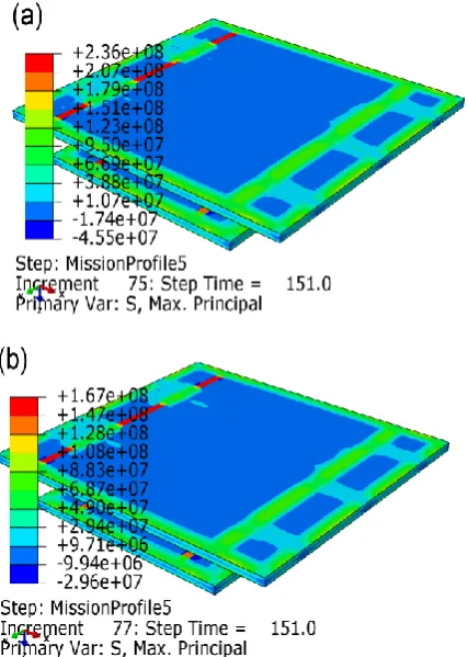
Fig. 14. Distributions of: (a) von Mises stress with unit in Pa; and (b) creep strain in most solder joints in the design CMB13 after 5 thermal cycles.
B.2 Effect of thermal history
The assembly has been subjected to relatively high temperatures for longer durations during the 5 thermal cycles than the 5 cycles of the mission profile. Relatively high temperatures (at longer duration) would promote creep strain accumulation, which would somewhat lead to the release of stress. Therefore it is not surprising that the mission profile and thermal cycling histories have significantly different effects on the stress and strain development in the parts/components of the assembly. For all the design cases listed in Table I, the relevant maximum stresses and strains in the different parts/components have all been observed at the corners and/or edges of the interfaces between the different materials, irrespective of the applied profile (mission or thermal). This can be understood because the stress and strain developments are caused by the mismatches in the CTEs of the different materials in the assembly. It should be pointed out that for all solder joints, the maximum von Mises stresses and creep strain accumulations occur in the solder joints between the bumps and IGBTs during the mission profile (Fig. 10). However, they occur in the solder joints between the
bumps and DBC substrates during the thermal cycles (Fig. 14). This can be attributed to the relatively high temperatures in the solder joints (used to join bumps) on Si chips when compared to those in the solder joints (used to join bumps) on the DBC substrates during the mission profile, compared to the uniform distribution of temperatures during thermal cycling. The solder joints with the maximum creep strain accumulations are in general identified as the thermo-mechanically weak point [23]. Therefore, as stated in previous work [32], care must be taken when the results of thermal cycling are used to predict the failure and lifetimes of assemblies during realistic mission profiles.
Fig. 15. Comparison of the evolutions of the maximum von Mises stresses in the solder joints in all the design cases during: (a) 5 cycles of the mission profile; and (b) 5 thermal cycles.
[image:9.595.322.541.221.532.2]maximum-10
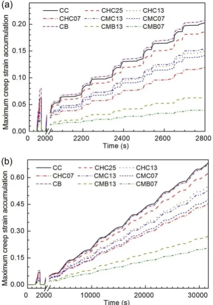
principal stresses in the AlN tiles of the DBC substrates occurduring cooling down of the thermal cycling from the highest temperature to the lower temperature. During both the mission profile and thermal cycling, the increase in rate for the maximum creep strain accumulation in all the solder joints is higher for higher maximum temperatures in the assembly (Figs. 6, 9 and 16). The latter can be attributed to the fact that the Sn-3.5Ag solder alloy is prone to creep at relatively high temperatures [10], [24].
Fig. 16. Comparison of the evolutions of the maximum creep strain accumulations in the solder joints in all the design cases during: (a) 5 cycles of the mission profile; and (b) 5 thermal cycles.
B.3 Effects of bump shapes and materials
From Figs. 15 to 17, it can further be seen that between the Cu cylinder bumps and Cu brick bumps (design cases CC and CB), the effects of these two types of bump shapes on the maximum von Mises stresses and creep strain accumulations in all the solder joints and the maximum maximum-principal stresses in the AlN tiles of the DBC substrates are all negligible during both the mission profile and the thermal cycling. This may be due to the fact that the solder joints with a higher CTE directly contact and withstand the different thermal expansion/contraction developments of the DBC substrates, Si chips and Cu bumps with relatively low CTEs. On the one hand, the individual solder joints for joining the cylinder bumps are thicker (on average), and may contribute more to the relevant stress and strain developments at the interfaces between them and the DBC substrates, Si chips and Cu bumps. On the other hand, the individual solder joints for joining the brick bumps are thinner in average thicknesses, and may transfer more relevant stresses and strains between the
two opposite interfaces of the corresponding solder joints. These two effects may counteract the effects of the two types of bump shapes on the relevant stress and strain developments in all the solder joints and the DBC substrates.
Fig. 17. Comparison of the evolutions of the maximum maximum-principal in the AlN tiles of the DBC substrates in all the design cases during: (a) 5 cycles of the mission profile; and (b) 5 thermal cycles.
Using relatively compliant Cu hollow cylinder bumps (design cases CHC25, CHC13 and CHC07), the maximum von Mises stresses and creep strain accumulations in all the solder joints can be reduced to some extent during both the mission profile and the thermal cycling. However, this somewhat increases the maximum maximum-principal stresses in the AlN tiles of the DBC substrates during both the mission profile and thermal cycling. These results may be associated with the fact that the compliant hollow bumps could absorb a certain amount of deformation energy from the solder joints, and transfer some to the AlN tiles of the DBC substrates. This is because a flexible PCB was reported to absorb some deformation energy of a flip chip assembly and thus slow the growth of cracks and improve the thermal fatigue lifetime of the corresponding solder joints subjected to thermal cycling [33].
[image:10.595.320.540.125.443.2] [image:10.595.53.272.186.498.2]11
expansion and contraction of the Cu/Mo shell/core compositecylinder bumps, and thus reduces the extent of mismatch of CTEs between the bumps, Si chips and DBC substrates.
More effectively, using the Cu/Mo/Cu composite brick bumps (design cases CMB13 and CMB07), the maximum von Mises stresses and creep strains in all the solder joints can further be reduced when compared with those using Cu/Mo shell/core composite cylinder bumps during both the mission profile and the thermal cycling. The relevant maximum stresses in the AlN tiles of the DBC substrates are also slightly lower than or similar to those using the Cu/Mo shell/core composite cylinder bumps. This can be ascribed to the fact that the Cu/Mo/Cu composite brick bumps can more effectively reduce the extent of mismatch of CTEs between the bumps, Si chips and DBC substrates than the Cu/Mo shell/core composite cylinder bumps.
V. EXPERIMENTAL EVALUATION
The above thermo-mechanical stresses and strains simulated using the FE numerical model are evaluated by comparison with the experimental results for the reliability of the design cases CHC25 and CMB13 subjected to thermal cycling between -55 ºC and +150 ºC as shown in Fig. 6. These two design cases have been tested because the simulated thermo-mechanical stresses and strains are easy to compare (showing a marked difference in values) and the corresponding bump materials are commercially available. The samples were prepared using two soldering steps as detailed previously. The reliability of the assembled samples during the thermal cycling test was continuously monitored by recording the on-state voltage drop across the Si chips under a fixed bias current of 200 mA. The related experimental procedures for this real-time monitoring and recording have been described in detail in a previous paper [34], and, thus, are not repeated here.
[image:11.595.327.537.216.704.2]Fig. 18. Evolutions of on-state voltage drops, V_IGBTs, across the IGBTs in the samples CHC and CMB13 at 90 ºC, with respect to number of thermal cycle between -55 ºC and 150 ºC.
Fig. 18 presents the evolutions of the on-state voltage drop recorded at 90 ºC, V_IGBTs, across the IGBTs in the samples CHC and CMB13, with respect to number of thermal cycles between -55 ºC and +150 ºC. Note that the recorded on-state voltage drop included the contributions from both the IGBTs themselves and the electronic interconnects such as the bumps,
solder joints and the Cu tracks on the DBC substrates. Therefore, any significant change in the recorded voltage drop should be associated with failure in the corresponding conductive path. As can be seen from Fig. 18, a 10% increase in the V_IGBT was recorded after 100 thermal cycles for the sample CHC25 and after 265 thermal cycles for the sample CMB13. Such a 10% increase in V_IGBT can be used as an indicator of the failure of the solder joints in the conductive path, due to the formation and initial rapid growth of fatigue cracks. This is because no appreciable degradation of the DBC substrates could contribute a 10% increase in V_IGBTs, while all the Si chips in the assemblies were intact.
[image:11.595.59.269.498.646.2]12
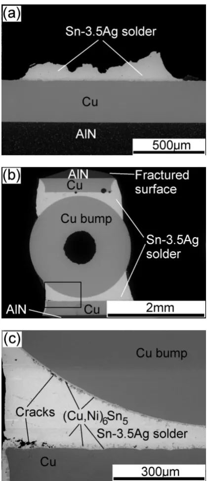
The thermal cycling test of the sample CHC25 was stoppedafter 550 cycles. Complete de-bonding of several bumps D from both the top and bottom DBC substrates and complete delamination of several Cu tracks from the AlN tiles of both the top and the bottom DBC substrates were observed. Fig. 19 shows some representative scanning electronic microscopy (SEM) images (backscattered) taken from the tested sample CHC25. The solder residual on the bottom DBC substrate as shown in Fig. 19 (a) is due to formation and growth of fatigue cracks within the solder joint used to join bumps D. The complete delamination of the two Cu tracks from both the top and the bottom DBC substrates shown in Fig. 19 (b) was due to the formation and growth of fatigue cracks within the AlN tiles. The enlarged view shown in Fig. 19 (c) confirmed the existence and growth of fatigue cracks within the solder joints prior to their fracture.
After 550 thermal cycles, no noticeable de-bonding of the soldered bumps and delamination of the DBC substrates could be observed in the sample CMB13. The thermal cycling test of this sample lasted until 770 cycles where partial delamination of the Cu tracks from the AlN tiles of the DBC substrates was observed. Fig. 20 shows typical fatigue cracks formed within the AlN tiles and the solder joints used to join bumps D between the two (top and bottom) DBC substrates in the
Fig. 20. SEM images taken from the sample CMB13 after 770 thermal cycles: (a) one bumps D between two Cu tracks on the AlN tiles of the top and the bottom DBC substrates, showing the fatigue cracks within the AlN tiles; and (b) enlarged view of the box at the bottom right side of (a), showing (Cu,Ni)6Sn5 IMC and fatigue cracks within the solder joint.
sample CMB13. Unlike sample CHC25, where some Cu tracks of the DBC substrates and some bumps D had been separated from the sample after 550 thermal cycles, all the Cu tracks and bumps still remained in the sample CMB13 after 770 thermal cycles. Therefore, it may be concluded that the two DBC substrates in sample CMB13 were more reliable than the two DBC substrates in sample CHC25 though exact lifetimes for them cannot be given in the present thermal cycling experiment.
Thermo-mechanical fatigue lifetimes of soft solder joints, such as the present Sn-3.5Ag solder joints can be described with prediction models based on plastic strain development, creep strain development and inelastic energy density per thermal cycle [10], [23]-[26]. In the present FE simulation, the mechanical property of the Sn3.5Ag solder joints was described by the Anand viscoplastic model, and the simulated creep strains include both the creep and plastic deformation developments in the solder joints subjected to thermal cycling. Combining the experimental lifetimes of 100 cycles and 256 cycles for the critical solder joints in the samples CHC25 and CMB13 with the simulated creep strain accumulations presented in Fig. 16b, the following equation can be applied through data fitting [23]:
cr f
C
N
1
(1)where Nf is the experimental fatigue lifetime in thermal cycles, cr the simulated creep strain accumulation per thermal cycle, C is the inverse of the creep ductility. With the cr of 0.132 and 0.056 for the samples CHC25 and CMB13, the present C=0.0683 is obtained. Such a value is comparable with but somewhat higher than the C=0.045 for the SnAgCu solder alloy reported in existing literature [23]. This may be attributed to the fact that the present Sn-3.5Ag solder joints had been saturated with Cu during the reflow process, as evident from the formation of (Cu,Ni)6Sn5 IMC within the solder joints as shown in Figs. 19(c) and 20(b). However, the present temperature range of thermal cycling from -55 °C to 150 °C is wider than those from -40 °C to 125 °C, -55 °C to 125 °C and 0 °C to 100 °C that were used in Ref. [23].
[image:12.595.56.271.367.693.2]13
Fig. 21. Experimental lifetimes and those predicted from the creepstrain accumulations per thermal cycle or per cycle of the mission profile, cr, simulated with the FE model.
There are two types of fatigue lifetime models which have been developed to predict the lifetimes of DBC substrates. One of them is based on the plastic strain development within the Cu metallization, either in the form of the Coffin-Manson law or in more complicated form [27], [28]. The other one is based on the maximum principal stress within the ceramic tiles, including the fracture mechanics modelling the propagation rate of crack and the weakest-link theory capturing the material’s probabilistic behaviour [21], [29]. From the present experimental result that the DBC substrates in the sample CMB13 was more reliable than those in sample CHC25, the simulated maximum principal stress within the AlN tiles should be more applicable to compare the lifetimes for optimization of design. This is because the simulated maximum plastic strains within the Cu metallization of the DBC substrates in the two samples were found to be almost the same as each other, but the simulated maximum principal stress within the AlN tiles of the DBC substrates in the sample CHC25 is somewhat higher than for that in sample CMB13 (Fig. 17).
Both the three-dimensional FE simulation results and the resultant thermal cycling experiment verify that the selection of Cu/Mo/Cu composite brick bumps in the designed power module can significantly improve the thermo-mechanical reliability of both the solder joints and the DBC substrates. As reflected by the simulation results shown in Figs. 15 to 17, both the shape and selection of material for the bumps are important to improve the thermo-mechanical reliability of all the solder joints, DBC substrates and Si chips in a stacked substrate-chip-bump-chip-substrate assembly. The optimized reliability can be achieved by selecting the Cu/Mo/Cu composite brick bumps with the lowest thickness ratio of Cu to Mo.
VI. CONCLUSIONS
Based on the above results of the FE simulation and experimental evaluation for the thermo-mechanical reliability of the stacked substrate-chip-bump-chip-substrate assembly used to construct a highly integrated bi-directional power switch, the following conclusions are drawn:
Of the 9 design cases, the Cu brick bumps have the best thermal performance, and the Cu hollow cylinder bumps with
the thinnest thickness have the worst thermal performance. The Cu/Mo/Cu composite brick bumps showing optimized thermo-mechanical reliability of the assembly have thermal performance between the Cu brick bumps and the Cu hollow cylinder bumps, with a maximum temperature 1.5 °C higher than that in the assembly with the Cu brick bumps.
The initial stress and strain states in the DBC substrates have negligible effect on the stress and strain developments in the Sn-3.5Ag solder joints, but have a marked effect on the stress and strain developments in the DBC substrates. However, the different initial stress and strain states in the DBC substrates give similar relative results.
During both the mission profile and thermal cycling, the relevant maximum stress and creep strain developments reflecting the thermo-mechanical reliability of the Sn-3.5Ag solder joints and DBC substrates have the same or similar order when comparing the different bumps in the assembly. However, the maximum von Mises stresses and creep strain accumulations occur in solder joints used to join bumps on IGBTs during the mission profile, but occur in solder joints used to join bumps on DBC substrates during the thermal cycling tests.
The FE simulation results in combination with the accelerated thermal cycling experiment reveal that the thermo-mechanical reliability of the Sn-3.5Ag solder joints in the assembly samples with the Cu hollow cylinder bumps and the Cu\Mo\Cu composite brick bumps is inversely proportional to the creep strain accumulation per thermal cycle, and the thermo-mechanical reliability of the DBC substrate is more likely to be dominated by the maximum principal stress development within the AlN tiles.
The results from the accelerated thermal cycling experiment verifies that selection of the Cu/Mo/Cu composite brick bumps in the stacked substrate-chip-bump-chip-substrate assembly can significantly improve the thermo-mechanical reliability of both the solder joints and the DBC substrates when compared to Cu cylinder bumps and Cu hollow cylinder bumps reported in previous work.
ACKNOWLEDGEMENTS
The authors gratefully acknowledge the support of the Innovative Electronics Manufacturing Research Centre (IeMRC) funded by the UK Engineering and Physical Sciences Research Council (EPSRC) through research grant EP/H03014X/1.
REFERENCES
[1] C. Luechinger, “Ribbon Bonding – A Scalable Interconnect for Power QFN Packages,” in Proceedings of 9th Electronics Packaging Technology Conference, December 10-12, 2007, Singapore, pp. 47-54.
[2] G.Q. Lu, X. Liu, S. Wen, J.N. Calata, J.G. Bai, “Strategies for improving the reliability of solder joints on power semiconductor devices,” Soldering and Surface Mount Technology, vol. 16, issue 2, pp. 27-40, 2004.
[image:13.595.57.266.68.222.2]14
IEEE Transactions on Industry Applications, vol. 41,issue 6, pp. 1603-1611, November / December 2005. [4] Z. Liang, B. Lu, J.D. van Wyk, F.C. Lee, “Integrated
CoolMOS FET/SiC-Diode Module for High Performance Power Switching,” IEEE Transactions on Power Electronics, vol. 20, issue 3, pp. 679-686, May 2005. [5] J. Yin, Z. Liang, J.D. van Wyk, “High Temperature
Embedded SiC Chip Module (ECM) for Power Electronics Applications,” IEEE Transactions on Power Electronics, vol. 22, issue 2, pp. 392-398, March 2007. [6] N. Khan, S.W. Yoon, A.G.K. Viswanath, V.P. Ganesh, R.
Nagarajan, D. Witarsa, S. Lim, K. Vaidyanathan, “Development of 3-D Stack Package Using Silicon Interposer for High-Power Application,” IEEE Transactions on Advanced Packaging, vol. 31, issue 1, pp. 44-50, February 2008.
[7] J.N. Calata, J.G. Bai, X. Liu, S. Wen, G.Q. Lu, “Three-Dimensional Packaging for Power Semiconductor Devices and Modules,” IEEE Transactions on Advanced Packaging, vol. 28, issue 3, pp. 404-412, August 2005. [8] S. Haque, K. Xing, R.L. Lin, C.T.A. Suchicital, G.Q. Lu,
D.J. Nelson, D. Borojevic, F.C. Lee, “An Innovative Technique for Packaging Power Electronic Building Blocks Using Metal Posts Interconnected Parallel Plate Structures,” IEEE Transactions on Advanced Packaging, vol. 22, issue 2, pp. 136-144, May 1999.
[9] C.M. Johnson, C. Buttay, S.J. Rashid, F. Udrea, G.A.J. Amaratunga, P. Ireland, R.K. Malhan, “Compact Double-Side Liquid-Impingement-Cooled Integrated Power Electronic Module,” in Proceedings of the 19th International Symposium on Power Semiconductor Devices & ICs, May 27-30, 2007 Jeju, Korea, pp.53-56. [10] A. Zéanh, O. Dalverny, M. Karama, E. Woirgard, S.
Azzopardi, A. Bouzourene1, J. Casutt, M.M. Guyennet, “Thermomechanical Modelling and Reliability Study of an IGBT Module for an Aeronautical Application,” in Proceedings of 9th Int. Conf. on Thermal, Mechanical and Multiphysics Simulation and Experiments in Micro-Electronics and Micro-Systems, EuroSimE 2008, Freiburg-im-Breisgau, Germany, April 21-23, 2008. [11] L. Menager, M. Soueidan, B. Allard, V. Bley, B. Schlegel,
“A Lab-Scale Alternative Interconnection Solution of Semiconductor Dice Compatible with Power Modules 3-D Integration,” IEEE Transactions on Power Electronics, vol. 25, issue 7, pp. 1667-1671, July 2010.
[12] J. Lee, D.M. Fernandez, M. Paing, Y.C. Yeo, S. Gao, “Electroless Ni Plating to Compensate for Bump Height Variation in Cu–Cu 3-D Packaging,” IEEE Transactions on Components, Packaging and Manufacturing Technology, vol. 2, issue 6, pp. 964-970, June 2012. [13] E. Vagnon, P.O. Jeannin, J.C. Crébier, Y. Avenas, “A
Bus-Bar-Like Power Module Based on Three-Dimensional Power-Chip-on-Chip Hybrid Integration,” IEEE Transactions on Industry Applications, vol. 46, issue 5, pp. 2046-2055, September / October 2010. [14] A. Solomon, A. Castellazzi, R. Hoyland, P. Agyakwa,
J.F. Li, C.M. Johnson, “A highly integrated high-voltage bi-directional switch,” in Proceedings of 2009 International Semiconductor Device Research Symposium,ISDRS 2009, December 9-11, 2009, College
Park, MD, USA, 2009, Paper 38.
[15] A. Castellazzi, A. Solomon, P. Agyakwa, J.Li, A. Trentin, C.M. Johnson, “High power density, low stray inductance, double sided cooled matrix-converter type switch,” in Proceedings of International Power Electronics Conference (IPEC), June 21-24, 2010, Sapporo, Japan, pp. 528-533.
[16] A. Solomon, J.F. Li, A. Castellazzi, C.M. Johnson, “Integrated half-bridge switch using 70μm thin devices and hollow surface bumps,” in Proceedings of 4th Annual IEEE Energy Conversion Conference and Exposition (ECCE 2012 International Conference), September 15-20, 2012, Raleigh Convention Center, Raleigh, NC, USA, pp. 4254-4261.
[17] J.F. Li, A. Castellazzi, A. Solomon, C.M. Johnson, “Reliable integration of double-sided cooled stacked power switches based on 70 µm thin IGBTs and diodes,” in Proceedings of CIPS 2012, 7th International Conference on Integrated Power Electronics Systems, March 6-8, 2012, Nuremberg, Germany, pp. 131-136. [18] Z. Mei, “Microstructual evolution and interfacial
interaction in lead-free solder interconnects,” in Lead-Free Solder Interconnect Reliability, Edited by D. Shangguan, ASM International, 2005, pp. 29-66.
[19] Y.C. Gerstenmaier, A. Castellazzi, G.K.M. Wachutka, “Electrothermal Simulation of Multichip-Modules With Novel Transient Thermal Model and Time-Dependent Boundary Conditions,” IEEE Transactions on Power Electronics, vol. 21, issue 1, pp. 45-55, January 2006. [20] C.M. Johnson, A. Castellazzi, R. Skuriat, P. Evans, J.F.
Li, P.A. Agyakwa, “Integrated High Power Modules,” in Proceedings of CIPS 2012, 7th International Conference on Integrated Power Electronics Systems, March 6-8, 2012, Nuremberg, Germany, pp. 357-366.
[21] A. Zeanh, O. Dalverny, M. Karama, A. Bouzourene, “Lifetime and reliability assessment of AlN substrates used in harsh aeronautic environments power switch modules,” Advanced Materials Research, vol. 112, pp 113-127, May 2010.
[22] W.W. Sheng, R.P. Colino, Power Electronic Modules: Design and Manufacture, CRC Press LLC, Florida, USA, 2005.
[23] A. Syed, “Accumulated creep strain and energy density based thermal fatigue life prediction models for SnAgCu solder joints,” in Proceedings of ECTC 2004 Conference, Las Vegas, USA, 2004, pp.737-746.
[24] C. Andersson, Z. Lai, J. Liu, H. Jiang, Y. Yu, “Comparison of isothermal mechanical fatigue properties of lead-free solder joints and bulk solders,” Materials Science and Engineering A, vol. 394, pp. 20-27, March 2005.
[25] X. Chen, D. Zhou, “Modeling and Reliability Analysis of Lead-Free Solder Joints of Bottom Leaded Plastic (BLP) Package,” in Proceedings of 2006 Conference on High Density Microsystem Design and Packaging and Component Failure Analysis (Hdp '06), June 27-30, 2006, Shanghai University, Shanghai, China.
15
Journal of Central South University, vol. 16, issue 3, pp.0339−0343, June 2009.
[27] L. Xue, “A unified expression for low cycle fatigue and extremely low cycle fatigue and its implication for monotonic loading,” International Journal of Fatigue, vol. 30, issue 10-11, pp. 1691-1698, October / November 2008.
[28] G. Dong, X. Chen, X. Zhang, K.D.T. Ngo, G.Q. Lu, “Thermal fatigue behaviour of Al2O3-DBC substrates under high temperature cyclic loading,” Soldering & Surface Mount Technology, vol. 22, issue 2, pp. 43–48, 2010.
[29] L.J.M.G. Dortmans, G.D. With, “Weakest-link Failure Predictions for Ceramics Using Finite Element Post-processing,” Journal of the European Ceramic Society, vol. 6, issue 6, pp. 369-374, 1990.
[30] P.L. Larsson, A.E. Giannakopoulos, “Tensile stresses and their implication to cracking at pyramid indentation of pressure-sensitive hard metals and ceramics,” Materials Science and Engineering A, vol. 254, issue 1-2, pp. 268– 281, October 1998.
[31] A.G. Gracia, P. Roux, E. Woirgard, C. Zardini, “Influence of the thermo-mechanical residual state on the power assembly modellization,” Microelectronics Reliability, vol 44, issue 9-11, pp. 1331-1335, September-November 2004.
[32] R. Schmidt, U. Scheuermann, “Separating failure modes in power cycling tests,” in Proceedings of CIPS 2012, 7th International Conference on Integrated Power Electronics Systems, March 6-8, 2012, Nuremberg, Germany, pp. 97-102.
[33] X. Chen, Y.C. Lin, X. Liu, G.Q. Lu, “Fracture mechanics analysis of the effect of substrate flexibility on solder joint reliability,” Engineering Fracture Mechanics, vol. 72, issue 17, pp. 2628–2646, November 2005.
[34] T. Dai, J.F. Li, M. Corfield, A. Castellazzi, P. Wheeler, “Real-time degradation monitoring and lifetime estimation of 3D integrated bond-wire-less double-sided cooled power switch technologies,” in Proceedings of the 15th European Conference on Power Electronics and Applications, September 3-5, 2013, Lille, France, paper no. 0760.
Jianfeng Li received the B.S. degree in mineralogy from Nanjing University, Nanjing, China, in 1991, and the M.S. and Ph.D. degrees both in materials science from the Shanghai Institute of Ceramics, Chinese Academy of Sciences, Shanghai, China, in 1996 and 1999, respectively. He worked in the areas of thermal spray, laser materials processing, and high-temperature electronic packaging at the University of Technology of Belfort, Monbeliard, France, the University of Manchester, and King’s College, London, U.K., until 2007. He joined the Power Electronics, Machines and Control Group of the University of Nottingham in the UK in 2008. He is currently a Research Fellow, and working in packaging, assembling and manufacturing technologies for the development of high performance and low cost power electronics. His recent research interests include lead-free
solder alloys, transient liquid phase soldering, sintering of Ag nanoparticles, reliability of power electronic interconnects and planar power modules.
Alberto Castellazzi is Associate
Professor of Power Electronics at the University of Nottingham, Nottingham, UK. His research interests are characterisation, modelling, application, packaging and cooling of power devices. He has been active in power electronics research and development for over 15 years and has had extensive collaborations with major European and international industrial research laboratories and groups on publicly and privately funded research projects. He has authored and co-authored over 100 papers in peer reviewed specialist journals and conferences, for which he also regularly acts as a reviewer.
Dai Tianxiang received MEng degree in Electrical and Electronic Engineering from The University of Nottingham, Nottingham, United Kingdom, in 2014. He will start his first year PhD in University of Warwick and his area of research is silicon carbide MOSFET design and reliability.
Adane Kassa received the MEng
degree in Electrical and Electronic Engineering from The University of Nottingham, Nottingham, United Kingdom, in 2011 where currently works towards his PhD degree. His area of research is Advanced Packaging and Integration solution for enhanced performance power converters.
16
Professor C Mark Johnson (Membersince 1990) received the BA degree in engineering and the PhD degree in electrical engineering from the University of Cambridge, UK, in 1986 and 1991 respectively.
From 1990 to 1992 he was a Research Associate at the University of Cambridge and in 1992 he was appointed Lecturer at the University of Newcastle, UK, where his research included the design, analysis and characterisation of power semiconductor devices, resonant power conversion and instrumentation.
From 1998 to 2001 he managed the UK national programme on Silicon Carbide electronics and in 2000 he became Reader of Power
Electronics at the University of Newcastle. In 2003, Professor Johnson was appointed as Rolls-Royce/RAEng Research Professor of Power Electronic Systems at the University of Sheffield and in 2006 he was appointed to a personal chair at the University of Nottingham, where he leads research into power semiconductor devices, power device packaging, reliability, thermal management, power module technologies and power electronic applications.