This content has been downloaded from IOPscience. Please scroll down to see the full text.
Download details:
IP Address: 128.243.39.164
This content was downloaded on 12/01/2017 at 15:14
Please note that terms and conditions apply.
Automated extraction of single H atoms with STM: tip state dependency
View the table of contents for this issue, or go to the journal homepage for more 2017 Nanotechnology 28 075302
(http://iopscience.iop.org/0957-4484/28/7/075302)
Home Search Collections Journals About Contact us My IOPscience
You may also be interested in:
Single-atom reversible recording at roomtemperature U J Quaade, K Stokbro, R Lin et al.
Manipulation of polyatomic molecules with the STM: chlorobenzene/Si(111)-(7times7) P A Sloan and R E Palmer
Silicon-basedmolecular nanotechnology M C Hersam, N P Guisinger and J W Lyding
Controllable dissociations of PH3 molecules on Si(001) Qin Liu, Yanhua Lei, Xiji Shao et al.
Vibrational-Energy Redistribution in Single-Atom Manipulation by Scanning Tunneling Microscope Qiang Shi, Dehuan Huang and Qingshi Zhu
Nanoscale patterning and selective chemistry of silicon surfaces by ultrahigh-vacuum scanning tunneling microscopy
J W Lyding, T-C Shen, G C Abeln et al.
Molecular and atomic manipulation mediated by electronic excitation of the underlying Si(111)-7x7 surface
Kristina R Rusimova and Peter A Sloan
Lithography and doping in strained Si towards atomically precise device fabrication W C T Lee, S R McKibbin, D L Thompson et al.
Automated extraction of single H atoms with
STM: tip state dependency
Morten Møller
1, Samuel P Jarvis
1,4, Laurent Guérinet
2, Peter Sharp
1,
Richard Woolley
3, Philipp Rahe
1and Philip Moriarty
11
School of Physics and Astronomy, University of Nottingham, Nottingham, NG7 2RD, UK 2
Institut National des Sciences Appliquées de Toulouse, 135, Avenue de Rangueil - 31077, Toulouse, Cedex 4 France
3
Quantulus Technology Ltd, Fairway Road, Shepshed, Leicestershire LE12 9DS,UK 4
Physics Department and Materials Science Institute, Lancaster University, Lancaster LA1 4YB, UK
E-mail:[email protected]
Received 16 September 2016, revised 1 November 2016 Accepted for publication 2 November 2016
Published 11 January 2017
Abstract
The atomistic structure of the tip apex plays a crucial role in performing reliable atomic-scale surface and adsorbate manipulation using scanning probe techniques. We have developed an automated extraction routine for controlled removal of single hydrogen atoms from the H:Si
(100)surface. The set of atomic extraction protocols detect a variety of desorption events during scanning tunneling microscope(STM)-induced modification of the hydrogen-passivated surface. The influence of the tip state on the probability for hydrogen removal was examined by comparing the desorption efficiency for various classifications of STM topographs(rows, dimers, atoms, etc). Wefind that dimer-row-resolving tip apices extract hydrogen atoms most readily and reliably(and with least spurious desorption), while tip states which provide atomic resolution counter-intuitively have a lower probability for single H atom removal.
Keywords: scanning probe microscopy, STM, atomic manipulation, hydrogen desorption, tip state
(Somefigures may appear in colour only in the online journal)
1. Introduction
In scanning probe microscopy(SPM), the ability to image and perform atomic and molecular manipulation has unsurpris-ingly been shown to be critically dependent on the state of the tip. Since their invention in the eighties, these instruments have been invaluable for investigating and manipulating surfaces and adsorbates at the atomic scale. An especially important class of atomic manipulation tool is available via the scanning tunnelling microscope (STM), which has the capability to perform hydrogen resist lithography on H:Si
(100) surfaces [1–4] with single atom specificity [5]. This technique has been used to fabricate not only prototype but functional electronic devices, including quantum dots[6,7],
conducting wires[8], and single atom transistors[9], and has been elegantly exploited to generate and manipulate artificial molecular orbitals (arising from dangling bond (DB) inter-actions)at the Si(100)surface [10]. One of the main advan-tages of STM-induced depassivation of this type is that it allows atomic scale imaging in concert with the patterning process, thus offering a high degree of operational control.
With the ultimate goal of autonomously fabricating atomic scale structures, we have implemented the following protocols. In order to automate and control the H:Si(100) patterning process with single-atom specificity, a feedback-controlled lithography (FCL) approach based on the techni-que developed by Lyding et al [5] was implemented. By actively monitoring the STM feedback signal and controlling the desorption parameters during patterning, individual atoms can selectively and ‘autonomously’ be desorbed. Similar protocols for automated atom-precision lithography have been developed by Randall and co-workers at Zyvex Labs
Nanotechnology28(2017)075302(7pp) doi:10.1088/1361-6528/28/7/075302
Original content from this work may be used under the terms of the Creative Commons Attribution 3.0 licence. Any further distribution of this work must maintain attribution to the author(s)and the title of the work, journal citation and DOI.
[11]; the resulting control system, ZyVector, is now com-mercially available. We show that for the variant of the FCL technique we have adopted, robust detection of single deso-rption events is possible. More importantly, the automation protocols we have developed enable the systematic generation and analysis of thousands of hydrogen desorption events, which in turn have provided key insights into the role that the atomistic structure of the tip apex plays in the extraction process.
The STM desorbs hydrogen atoms through inelastic electron scattering mechanisms[2,3,12,13]. At conditions of relatively high current and low electron energy tunneling, such as those used in our experiments, the desorption mechanism involves multi-quantum vibrational excitations of the Si–H bond[2,12, 14–16]. (At higher electron energies electrons possess sufficient energy to directly promote an electron from the Si–H bonding state to its corresponding antibonding orbital.)Previous studies have demonstrated that the basic desorption process involves only a single Si–H bond which is vibrationally excited by tunnelling electrons[2,17]. Although the H:Si(100) surface [18–21], and the desorption mechanism[2,3,12,13], have been studied extensively, the influence of the tip state on the desorption process has hitherto not been examined in any depth. For example, while the desorption efficiency has been analyzed for different bias and current parameters [22], these experiments did not take the state of the tip into account. Theoretical studies of atomic force microscope-based atomic manipulation[23–25]clearly, and unsurprisingly, show that the atomistic detail of the tip termination plays a crucial role in the process.(Unlike STM-tip-induced desorption, however, AFM-based manipulation on Si(100) surfaces is mediated by direct chemical interaction.)
In this work, we examine the influence of the atomistic structure of the tip apex on the desorption efficiency for STM-induced H atom extraction. Through a detailed, systematic analysis of thousands of H atom desoprtion events, we show that tips that produce row-resolved STM topographs yield single atom desorption events more reliably than tip apices which generate either dimer-resolved or atomically-resolved images. Moreover, row-resolving tip apices also generate the smallest number of spurious desorption events. (This dependence of spurious hydrogen desorption on the tip state was postulated previously by Ballard et al [26]. Here we provide strong evidence to support their hypothesis.) This sensitivity of H atom extraction to the precise atomistic structure of the tip is a critical factor in ensuring the repro-ducibility and reliability of atomic scale engineering of hydrogen-passivated semiconductor surfaces.
2. Methods
Silicon samples cut from Si(100) wafers (n-type, 6 mΩcm) were used throughout our experiments. Samples were pre-pared in an ultra-high vacuum(UHV) chamber with a base pressure of 5×10⁻¹¹mbar or less. Low base pressures were obtained by baking the UHV chamber at 145°C twice over
prolonged periods (three to four days). The samples were outgassed for a minimum of 12 h at 600°C. Clean Si(100) 2×1 samples were obtained byflash heating to 1150°C for 10 s, followed by gradual cooling from 900°C(at a rate of
∼1°C s−1) to room temperature. For hydrogen passivation, the sample was exposed to atomic hydrogen, which is obtained by cracking molecular hydrogen using a Specs GmbH thermal gas cracker, positioned approximately 10 cm from the sample. H2 was introduced into the chamber,
through the gas cracker, until a pressure of 1×10⁻⁶ mbar was reached. The sample was exposed for 1 min (i.e. 60 Langmuirs). During exposure, the sample was held at a temperature of 360±20°C in order to achieve hydrogen-terminated Si(100)-2×1 surfaces and avoid other recon-structions (such as(3×1)).
Measurements were performed on an Omicron variable-temperature(VT)STM-AFM system with a MATRIX control system. All experiments were performed at room temperature
(RT). Tungsten tips were used for both STM imaging and hydrogen extraction. These were electrochemically etched and subsequently annealed to 1000°C in the UHV cham-ber, in order to remove the oxide layer, before STM use. In order to randomize our statistics, the tip apex was routinely prepared during STM imaging using voltage pulsing and controlled tip crashing. Atom tracking [27] was used to eliminate drift during all automated extraction routine trials, unless otherwise stated. All STM images presented in this article were obtained with a sample bias voltage of 1.6 V and a constant current of 10 pA.
3. Results
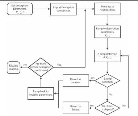
Figure 1 shows a flow diagram of the automated DB gen-eration routine. Upon activation of the automation routine, the tip was positioned at the desired location for atom extraction, and the initial parameters were subsequently changed to the desired desorption parameters VD, ID. Upon reaching the
desorption parameters, theZ(t)feedback signal is then used to monitor in real-time for a jump inZ. A threshold jump height of 0.3 Åwas found most suitable for detecting a desorption event, as higher thresholds potentially lead to desorption events not being detected, while smaller thresholds increase the probability of false detections. If a step inZ(Zstep0.3Å)
is detected, the desorption parameters subsequently rebound to the initial scan parameters. For step detection, a 10 ms integration time was found to be most appropriate as larger integration times could lead to multiple desorption events. Figure2shows a typicalz-jump detection event, including the full voltage- and current-ramp-related changes in thez posi-tion, for generation of a single DB.
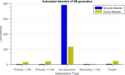
The automated extraction routine can be used for arbi-trary patterning with highfidelity as shown infigure3, where the extraction routine is used to atomically generate a 4×4 array of DBs. The reliability of the automated extraction routine was evaluated by comparing step detections from the routine with the true outcome as observed from STM ima-ging. The results are plotted in figure 4, for 1126 trials. For
2
each trial, the extraction routine is run for 60 s using similar desorption parameters. Desorption events are classified based on whetheranydesorption occurs directly underneath the tip
(primary)or if noneoccurs directly underneath the tip. Des-orption events with either an uncertain number, or more than four DBs generated, are collectively called clusters. Wefind that our step detection algorithm reliably detects any type of desorption, whether they occur directly underneath the tip
(primary) or not, but elsewhere (secondary). Single atom extraction events are detected with a 90% accuracy. Other unwanted events, such as multiple desorption events, or secondary desorptions, are similarly reliably detected. Unfortunately, the automated desorption algorithm does, unavoidably, occasionally register false jumps. This is mainly due to a combination of noise in Z and a low Z-threshold value. As discussed below, the tip state plays a key role in triggering false detection events.
It is well known that the structure of the tip can change during a desorption event as a result of tip–surface interac-tions [4]. To investigate the desorption efficiency under practical conditions, data containing tip changesduring des-orption were not excluded. Only a small subset(8.9%)of the
total number of trials involved tip-state changes. All tip imaging states were classified based on the image observed prior to desorption. Only data that could not be classified into the four tip imaging states (row, dimer, atom, asymmetric)
prior to desorption were excluded (constituting 1.7% of trials).
The dependence of the desorption efficiency on the ato-mistic structure of the tip apex was determined by grouping the tip states into a set of broad classes. Figures5(a)–(d)show a selection of observed tip states, and their respective grouping into the following classes:(a)rows,(b)dimers,(c) atomic, and (d)asymmetric.
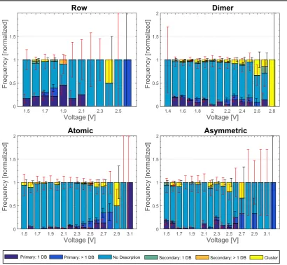
[image:4.595.79.527.61.437.2]The desorption efficiency is plotted in figure 6 as a function of voltage, for each respective type of observed tip states((a)row,(b)dimer,(c)atomic, and(d)asymmetric). All tip states that could be classified into these groupings(2023 out of 2074 trials)were included in our analysis. Each data value in thefigure corresponds to an experimental run of the automated extraction routine. In order to gauge the desorption efficiency as a function of voltage, all data were acquired by keeping the desorption parametersfixed(1.2 nA,Vfixed)for a given bias for the same amount of time (60 s). All
experimental trials performed at each voltage value (Vfixed)
were therefore normalized to 1. Data where false detections occurred before 60 s were excluded.
We observe that the onset of desorption follows the gen-eral tip classification rule: VrowVdimer,VasymmetricVatomic
for a given bias, respectively. This translates into a desorption probability that follow the same rule: ProwPdimer,
Pasymmetric Patomic. These results are further corroborated by
similarfindings using other STM tips and using different FCL automation routines(not included).
4. Discussion
[image:5.595.148.469.66.222.2]Our findings show that row-resolved tip states produce a single desorption event more reliably than other tip states, and
[image:5.595.53.547.272.369.2]Figure 2.The feedback(z)for automated DB generation performed atfixed position.(I)moved to position,(II)rampingID,(III)rampingVD, (IV)Zjump detection atID,VD,(V)rampVDback to imaging parameter,(VI)ID, and(VII)reached imaging parameters.
Figure 3.Successive single desorption events showing dangling bond formation using automated extraction routine. In images(a)–(d), each white‘x’represents the coordinates which were input to the H extraction algorithm. Sequential application of the algorithm produced the 4×4 dangling bond array shown in(e).VD=2 V,ID=250 800 pA– .
Figure 4.Detection efficiency for different desorption types using the automated detection algorithm. Here,primaryrefers to the generation of at least one dangling bond directly underneath the tip(preselected desorption coordinate), whilesecondaryis used whennodesorption occurs underneath the tip(but occurs elsewhere).Clustersrefers to the generation of more than four dangling bonds(DBs)or an indistinguishable number of DBs.
4
[image:5.595.168.432.439.597.2]that other unwanted reactions(such as producing clusters)are less likely for the row-resolving tip apex than for other states. The reason for this remains as yet unclear but an obvious candidate explanation relates to the density of states of the tip apex. Although the STM image contrast mechanism has been investigated for bare[28,29], and passivated Si(100)surfaces
[30,31], this has been in the context of the density of states and band structure of the substrate; the influence of the ato-mistic structure of the tip on the contrast mechanism has not yet been investigated.
For our desorption conditions(electron energies<4 eV), the dominant desorption mechanism is attributed to inelastic scattering of the tunneling electrons with the Si–H bond
[2, 12]. Using this model, the tunneling probability is dependent on several factors, including, of course, the local density of states(LDOS)of the tip. It is therefore reasonable to speculate that for the H:Si(100)surface, tip states produ-cing row-like STM topographs might have a greater density of states (in the energy window defined by the tip–sample bias)than other classes of tip apex. This will directly affect the available flux of electrons and, thus, the desorption probability.
Although early theoretical studies suggested that while the electricfield under the tip is insufficient to directly induce H atom desorption, it could nonetheless play a significant role via spatial localization of the excitation [14]due to a Stark effect. However, subsequent experiments, where neighboring hydrogen atoms were extracted, show that interdimer
extraction is more favorable than intradimer extraction, sug-gesting that the presence of an electric field does not play a significant role in the desorption process [17]. Our results support these latter findings. Moreover, wefind that the dis-tribution of different types of neighboring desorption events is also tip-state dependent, where intradimer desorption occurs more frequently for atomically resolved STM topographs. We are planning a systematic combined density functional theory
(DFT)-non-equilibrium Greens function study in order to elucidate the origin of the higher desorption efficiency of the row-resolving class of tip apices(and to ascertain the extent to which the H desorption process is mediated by the structure and density of states of the tip apex).
[image:6.595.45.549.65.345.2]Ourfindings have shown that extracting single H atoms is best achieved for row-resolving tip imaging states and low bias voltages. Additionally, at these conditions, undesirable side effects such as multiple or secondary desorptions are also minimized. The low bias voltage probably plays a significant role in limiting the number of unwanted desorption events as the yield is highly dependent on the the bias voltage and electron dosage [2–4]. Based on our findings we conclude that the best strategies for controlling the automated pattern-ing process can be obtained by (I) carefully selecting the proper tip geometries for desorption, (II) controlling the desorption yield (affected by desorption parameters, tip– sample distance), and (III) through reliable detection of H extraction by either minimizing/excluding noise influences or improving the step detection algorithm.
5. Conclusions
We have implemented an automated extraction routine cap-able of implementing and detecting single H atom desorption from H:Si(100)surfaces with high reliability. The routine was used to examine the influence of the tip state on the deso-rption efficiency by desorbing atoms using fixed desorption parameters, for a fixed time. Tip states were classified into four broad types: row-resolving, atom-resolving, dimer-resolving, and‘asymmetric’and their desorption efficiencies compared. Wefind that tips that produced row-resolved STM topographs desorb H atoms most efficiently. Our results are used to propose strategies for controlling the accuracy of single H atom extraction. Future work will focus on eluci-dating the origin of the tip state dependency of the desorption process via a combined density functional theory (DFT) -Greenʼs function approach.
Acknowledgments
This work was supported by the Engineering and Physical Sciences Research Council[grant numbers EP/G007837/1, EP/J500483/1], PM thanks the Engineering and Physical
Sciences Research Council for a Leadership Fellowship award which supported some of this work(EP/G007837/1) and SPJ was funded via an EPSRC PhD+fellowship (EP/ J500483/1); MM is grateful for the award of a Marie Curie fellowship funded by the ACRITAS FP7 initial training net-work (www.acritas.eu) under the Marie Skodowska-Curie Actions, project reference ACRITAS-317348-Ares(2016) 909492. MM also thanks John Randall, James Owen and colleagues at Zyvex Labs (Richardson, Texas)for hosting a month-long secondment during which he gained valuable insights into automated scanning probe lithography of H:Si
(100)surfaces. A significant amount of the research was also funded by the the European Commission’s FP7 ICTFET programme via the Atomic Scale and Single Molecule Logic gate Technologies(AtMol)project, Contract No. 270028. SPJ was funded via a Leverhulme Trust Early Career Fellowship, ECF-2015-005.
References
[image:7.595.97.508.62.440.2][1] Lyding J W, Shen T-C, Hubacek J S, Tucker J R and Abeln G C 1994 Nanoscale patterning and oxidation of H-passivated Si(100)-2×1 surfaces with an ultrahigh
Figure 6.Desorption frequency for each desorption type as a function of voltage for different tip imaging states. Each data point corresponds to a run of the automation routine over afixed voltage valueVfixed(normalized to 1 for eachVfixedvalue)for 60 s.
6
vacuum scanning tunneling microscopeAppl. Phys. Lett.64 2010–2
[2] Shen T-C, Wang C, Abeln G C, Tucker J R, Lyding J W, Avouris Ph and Walkup R E 1995 Atomic-scale desorption through electronic and vibrational excitation mechanisms
Science2681590–2
[3] Foley E T, Kam A F, Lyding J W and Avouris Ph 1998 Cryogenic UHV-STM study of hydrogen and deuterium desorption from Si(100)Phys. Rev. Lett.801336–9
[4] Soukiassian L, Mayne A J, Carbone M and Dujardin G 2003 Atomic wire fabrication by STM induced hydrogen desorptionSurf. Sci.528121–6
[5] Hersam M C, Guisinger N P and Lyding J W 2000 Silicon-based molecular nanotechnologyNanotechnology1170–6
[6] Fuechsle M, Mahapattra S, Zwanenburg F A, Friesen M, Eriksson M A and Simmons M Y 2010 Spectroscopy of few-electron single-crystal quantum dotsNat. Nanotechnol. 5502–5
[7] Haider M B, Pitters J L, DiLabio G A, Livadaru L and Wolkow R A 2008 Controlled coupling and occupation of silicon atomic quantum dots at room temperaturePhys. Rev. Lett.102046805
[8] Weber Bet al2012 Ohmʼs law survives to the atomic scale
Science33564–7
[9] Fuechsle M, Miwa J A, Mahapatra S, Ryu H, Lee S, Warschkow O, Hollenberg L C L, Klimeck G and Simmons M Y 2012 A single-atom transistorNat. Nanotechnol.7242–6
[10] Schofield S R, Studer P, Hirjibehedin C F, Curson N J, Aeppli G and Bowler D R 2013 Quantum engineering at the silicon surface using dangling bondsNat. Commun. 41649
[11] Ballard J B, Sisson T W, Owen1 J H G, Owen W R, Fuchs E, Alexander J, Randall J N and Ehr J R V 2013 Multimode hydrogen depassivation lithography: a method for optimizing atomically precise write timesJ. Vac Sci. Technol.B3106FC01
[12] Stokbro K, Thirstrup C, Sakurai M, Quaade U, Hu B Y-K, Perez-Murano F and Grey F 1998 STM-induced
hydrogen desorption via a hole resonancePhys. Rev. Lett.80 2618–21
[13] Thirstrup C, Sakurai M, Nakayama T and Stokbro K 1999 Temperature suppression of STM-induced desorption of hydrogen on Si(100)surfacesSurf. Sci.424L329–34
[14] Shen T-C and Avouris Ph 1997 Electron stimulated desorption induced by the scanning tunneling microscopeSurf. Sci.390 35–44
[15] Avouris Ph, Walkup R E, Rossi A R, Akpati H C,
Nordlander P, Shen T-C, Abeln G C and Lyding J W 1996 Breaking individual chemical bonds via STM-induced excitationsSurf. Sci.363368–77
[16] Soukiassian L, Mayne A J, Carbone M and Dujardin G 2003 Atomic-scale desorption of H atoms from the Si(100)-2×1: H surface: inelastic electron interactionsPhys. Rev.B68 035303
[17] Tong X and Walkow R A 2006 Electron-induced H atom desorption patterns created with a scanning tunneling microscope: Implications for controlled atomic-scale patterning on H-Si(100)Surf. Sci. Lett600L199–203
[18] Boland J 1990 Structure of the H-saturated Si(100)surface
Phys. Rev. Lett.653325–8
[19] Boland J 1993 Scanning tunnelling microscopy of the interaction of hydrogen with silicon surfacesAdv. Phys.42 129–71
[20] Dürr M and Höfer U 2006 Dissociative adsorption of molecular hydrogen on silicon surfacesSurf. Sci. Rep.61 465–526
[21] Raza H 2007 Theoretical study of isolated dangling bonds, dangling bond wires, and dangling bond clusers on a H:Si(001)-(2×1)surfacePhys. Rev.B76 045308
[22] Chen S, Xu H, Goh K E J, Liu L and Randall J N 2012 Patterning of sub-1 nm dangling-bond lines with atomic precision alignment on H:Si(100)surface at room temperatureNanotechnology23275301
[23] Jarvis S, Sweetman A, Bamidele J, Kantorovich L and Moriarty P 2012 Role of orbital overlap in atomic manipulationPhys. Rev.B85235305
[24] Yurtsever A, Sugimoto Y, Tanaka H, Abe M, Morita S, Ondráček M, Puo P, Pérez R and Jelinek P 2013 Force mapping on a partially H-covered Si(111)-(7×7)surface: influence of tip and surface reactivityPhys. Rev.B87 155403
[25] Ŝtich I, Tóbik J, Pérez R, Terakura K and Ke S H 2000 Tip– surface interactions in noncontact atomic force microscopy on reactive surfacesProg. Surf. Sci.64179–91
[26] Ballard J Bet al2014 Pattern transfer of hydrogen depassivation lithography patterns into silicon with atomically traceable placement and size controlJ. Vac Sci. Technol.B32041804
[27] Rahe P, Schütte J, Schniederberend W, Reichling M, Abe M, Sugimoto Y and Kühnle A 2011 Flexible drift-compensation system for precise 3D force mapping in severe drift environmentsRev. Sci. Instr.82063704
[28] Dubois M, Perdigão L, Delerue C, Allan G, Grandidier B, Deresmes D and Stiévenard D 2005 Scanning tunneling microscopy and spectroscopy of reconstructed Si(100) surfacesPhys. Rev.B71165322
[29] Perdigão L, Deresmes D, Grandidier B, Dubois M, Delerue C, Allan G and Stiévenard D 2004 Semiconducting Surface Reconstructions of p-type Si(100)substrates at 5 KPhys. Rev. Lett.92216101
[30] Suwa Y, Matsuura S, Mujimori M, Heike S, Onogi T, Kajiyama H, Hitosugi T, Kitazawa K, Uda T and Hashizume T 2003 Dopant-pair structures segregated on a hydrogen-terminated Si(100)surfacePhys. Rev. Lett.90 156101