Marcel Spurny
A Thesis Submitted for the Degree of PhD at the
University of St. Andrews
2011
Full metadata for this item is available in Research@StAndrews:FullText
at:
http://research-repository.st-andrews.ac.uk/
Please use this identifier to cite or link to this item: http://hdl.handle.net/10023/2111
This item is protected by original copyright
Chalcogenide Glasses
Marcel Spurny
Thesis submitted for the degree of Doctor of Philosophy
work carried out by me and that it has not been submitted in any previous application for a higher degree.
I was admitted as a research student in October, 2007 and as a candidate for the degree of Doctor of Philosophy in October 2007; the higher study for which this is a record was carried out in the University of St Andrews between 2007 and 2011.
Date ... signature of candidate ...
I hereby certify that the candidate has fulfilled the conditions of the Resolu-tion and RegulaResolu-tions appropriate for the degree of Doctor of Philosophy in the University of St Andrews and that the candidate is qualified to submit this thesis in application for that degree.
Date ... signature of supervisor ...
The following is an agreed request by candidate and supervisor regarding the electronic publication of this thesis:
Access to printed copy and electronic publication of thesis through the Uni-versity of St Andrews.
Date ...
Acknowledgements
During my PhD I had the privilege to work with many great people whom I would like to thank.
First of all, I would like to thank my supervisor Prof. Thomas Krauss for the great guidance and advice along my project. I would like to thank Dr. Marc Sorel and Dr. David Rogers for being my PhD examiners.
I would also like to thank all the members and former members of the group for the co-operation and friendship. I have to thank especially: Dr. William Whelan-Curtin (the only scientist I know with a nom de plume ;-)), Dr. Tom White, Dr. Daryl Beggs, Karl Welna, Isabella Rey, Emiliano Rezende Martins, Mark Scullion, Dr. Khaled Mnaymneh and Dr. Marco Grande.
This work would be nothing without the support of two great techni-cians, George Robb and Steve Balfour, who always managed to fix gear that ”accidentally” broke.
I would like to thank David Steven and Callum Smith from the mechanical workshop for the help with buidling the etching machine. Furthermore I would like to thank Mark Ross from electronics workshop with the great help with all the electronics. A great thanks also goes to Scott Johnston, thanks for the golfing lesson.
Apart from working with people in St Andrews I was working great sci-entist in Australia and Italy whom I have to thank a lot. I have to thank the group of Prof. Ben Eggleton at the University of Sydney, especially Dr. Christelle Monat, Dr. Christian Grillet, Michael Lee, Bill Corcoran for working with me on the chalcogenides and especially for doing the THG mea-surements. Also I would like to thank Dr. Christian Karnutsch (now Prof. Dr. ;)), whom I met in Sydney for inspiring me.
At the Australia National University, I would like to thank Prof. Barry Luther-Davies and his group for supplying me with the chalocgenide wafers, especially Dr. Steve Madden, Douglas Bulla and Dr. Duk Yong-Choi.
At the University of Pavia, I would like to thank Dr. Matteo Galli for the resonance scattering experiments.
Finally, and most importantly, I would like to thank my family. I would like to thank my father Helmut, my mother Monika, my sister Manuela and my second cousin Norbert for all their love and support I have had throughout the years. Tausend Dank für alles!
The growing speed and bandwidth requirements of telecommunication sys-tems demand all-optical on-chip solutions. Microphotonic devices can deliver low power nonlinear signal processing solutions. This thesis looks at the slow light photonic crystals in chalcogenide glasses to enhance low power nonlinear operation.
I demonstrate the development of new fabrication techniques for this deli-cate class of materials. Both, reactive ion etching and chemically assisted ion beam etching are investigated for high quality photonic crystal fabrication. A new resist-removal technique was developed for the chemical, mechanical and light sensitive thin films.
I have developed a membraning method based on vapor phase etching in combination with the development of a save and economical etching tool that can be used for a variety of vapour phase processes.
Dispersion engineered slow light photonic crystals in Ge33As12Se55are de-signed and fabricated. The demonstration of low losses down to21±8dB/cm is a prerequisite for the successful demonstration of dispersion engineered slow light waveguides up to a group index of around ng ≈40.
The slow light waveguides are used to demonstrate highly efficient third harmonic generation and the first advantages of a pure chalcogenide system over the commonly used silicon. Ge11.5As24Se64.5 is used for the fabrication of photonic crystal cavities. Quality factors of up to 13000 are demonstrated. The low nonlinear losses have enabled the demonstration of second and third harmonic generation in those cavities with powers up to twice as high as possible in silicon.
A computationally efficient model for designing coupled resonator band-pass filters is used to design bandband-pass filters. Single ring resonators are fabricated using a novel method to define the circular shape of the rings to improve the fabrication quality. The spectral responses of the ring resonators are used to determine the coupling coefficient needed for the design and fab-rication of the bandpass filters. A flat top bandpass filter is fabricated and characterized as demonstration of this method.
Journal Papers
1. M. Spurny, L. O’Faolain, D. A. P. Bulla, B. Luther-Davies and T.
F. Krauss, Fabrication of low loss dispersion engineered chalcogenide photonic crystals, Optics Express 19(3) 1991-1996 (2011).
2. M. Grande, L. O’Faolain, T. P. White, M. Spurny, A. D’Orazio, T. F. Krauss,Optical filter with very long stopband (approxiamate to 300nm) based on a photonic-crystal vertical-directional coupler, Optics Letters
34(21) 3292-3294 (2009).
Conference Papers
1. C. Monat, M. Spurny, C. Grillet, L. O’Faolain, T. F. Krauss, B. J.
Eggleton, D. A. P. Bulla, S. Madden, B. Luther-Davies,Third-harmonic generation in slow light dispersion engineered photonic crystal
waveg-uides in chalcogenides, CLEO 2011.
2. M. Spurny, T. F. Krauss, C. Monat, B. J. Eggleton, S. Madden, D. Y. Choi, D. A. P. Bulla, B. Luther-Davies,Dispersion Engineering in Low
3. M. Spurny, B. Corcoran, C. Monat, T. F. Krauss, Slow Light enhanced
nonlinear photonic functionalities, SPIE, 2010.
4. M. Spurny, T. F. Krauss, Prospects for Chalcogenide Photonic Crystals
in Nonlinear Optics: Towards All Optical Regeneration, presented at
IOP Nonliner Optics and Communciations (2009).
5. M. Spurny, L. O’Faolain, T. P. White, T. F. Krauss, Fabrication of photonic crystal waveguides in chalcogenide glasses, PECS-VIII (2009).
AWARDS
Contents
Publications 8
1 Introduction and state of the art 17
1.1 Goals . . . 17
1.2 Intensity enhanced nonlinear optics . . . 19
1.3 From fibers to microphotonics . . . 24
1.3.1 Light localization in periodic structures . . . 26
1.3.2 Photonic cystals as ultracompact waveguides . . . 29
1.3.3 The limits of silicon and the search for other materials 30 1.3.4 Chalcogenide glasses as a new type of nonlinear material 34 1.3.5 State-of-the-art - applications of chalcogenides and com-parison with silicon . . . 35
1.4 Summary . . . 38
2 Dispersion Engineered Chalcogenide Photonic Crystals 39 2.1 Theory . . . 39
2.1.1 2D photonic crystal waveguides in silicon and chalco-genides . . . 39
2.1.3 Effects of slow light on the mode area and nonlinear
response . . . 47
2.1.4 Conclusions . . . 48
2.2 Photonic crystal fabrication . . . 48
2.2.1 Pre-processing . . . 49
2.2.2 Chemical sensitivity . . . 52
2.2.3 Light induced changes . . . 54
2.2.4 Electron-beam resists . . . 56
2.2.5 Electron-beam writing . . . 57
2.2.6 Proximity Error Correction . . . 57
2.2.7 Anisotropic etching of chalcogenide glass thin films . . 63
2.2.8 Reactive Ion Etching of chalcogenide glass photonic crystals . . . 65
2.2.9 Chemically Ion Beam Etching of chalcogenide glass photonic crystals . . . 67
2.2.10 Taper design and underetching . . . 71
2.3 Conclusions . . . 73
3 Bandpass filter based on coupled ring resonators 75 3.1 Overview . . . 75
3.3 Filter design . . . 78
3.4 Determination of the coupling coefficients . . . 81
3.5 Cascaded rings . . . 82
3.6 Fabrication of silicon ring resonators . . . 85
3.7 Characterization of silicon ring resonator bandpass filters . . . 87
3.8 Bandpass filter . . . 93
3.9 Ring resonators in chalcogenide glasses . . . 94
3.10 Conclusions . . . 95
4 Vapour phase etching 96 4.1 Vapour phase etching of silicon dioxide . . . 98
4.2 Operating principle of the machine . . . 98
4.2.1 Silicon degradation . . . 100
4.3 A stable and versatile vapour phase etching tool . . . 101
4.3.1 Aims of the tool . . . 101
4.3.2 Working principle . . . 101
4.3.3 Chamber design . . . 102
4.3.4 Chamber performance . . . 105
4.3.5 Electronics . . . 107
4.3.6 Programming Interface . . . 109
4.5 Conclusions . . . 111
5 Characterization 112 5.1 Transmission measurements and refractive index determina-tion of AMTIR-1 photonic crystal waveguides . . . 112
5.2 Loss measurements . . . 114
5.3 Dispersion measurements . . . 115
5.4 Conclusions . . . 117
6 Red and green light emission from chalcogenide photonic crystal structures 118 6.1 Second and third harmonic generation in slow light photonic crystal waveguides and cavities . . . 118
6.2 Third Harmonic Generation in AMTIR-1 Slow Light Photonic Crystal Waveguides . . . 120
6.3 Second and Third Harmonic Generation in chalcogenide cavities124 6.4 Conclusions . . . 129
7 Conclusions 130 A Appendix 133 A.1 Definitions . . . 133
A.1.2 Kerr Effect . . . 133
A.1.3 Four-Wave Mixing . . . 133
A.1.4 Degenerate Four-Wave Mixing . . . 134
A.1.5 Cross-Phase Modulation . . . 134
A.1.6 Supercontinuum Generation . . . 134
A.1.7 Highly nonlinear fiber . . . 135
A.1.8 Directional coupler . . . 135
A.1.9 Two-photon absorption (TPA) . . . 135
A.1.10 Mach-Zender Interferometer . . . 135
A.1.11 Thin films . . . 136
A.1.12 Rib waveguide . . . 136
A.1.13 Access waveguide . . . 137
A.1.14 CMOS . . . 137
A.1.15 Reciprocal lattice . . . 138
A.1.16 Total Internal Reflection . . . 138
A.1.17 Line defect . . . 139
A.1.18 Add-drop filter . . . 140
A.1.19 Bandpass filter . . . 140
A.1.20 Cauchy-Lorentz Distribution . . . 141
A.1.21 Racetrack resonator . . . 141
A.1.23 Cutback measurements . . . 142
A.2 A 2R all-optical regnerator in chalcogenides . . . 142
A.2.1 Theory of self phase modulation . . . 144
A.2.2 Pulse propagation in photonic crystal waveguides . . . 147
A.2.3 Split-Step-Fourier Method . . . 149
A.2.4 Pulse propagation . . . 151
A.2.5 The nonlinear transfer function . . . 153
A.2.6 Summary and Conclusions . . . 154
List of figures 156
List of tables 160
1
Introduction and state of the art
1.1
Goals
Optical communication networks require fast optical packet switches and regenerators for routing and transmitting optical data packages. Today’s fastest optical packet switches work at speeds of up to 40Gbit/s. These speeds can only be achieved using slower electronics that operate in parallel [1]. These systems typically have a power consumption of around 10kW and a footprint of around 0.5m2. An optical regenerator, for example the Cisco OC-48/STM-16 [2], that works at the same speed still uses around
0.13m2 of space and has a heat dissipation of 100W. Taking into account that optical regeneration is necessary for every80kmof fiber in the network, the total energy consumption and excess heat is immense. The demand for increasing speed and bandwidth requires faster solutions with lower power consumption and smaller footprints. All-optical solutions can provide both
faster processing speed and lower power consumption, since the opto-electro-opto conversion is cut-out of these schemes. Most all-optical regeneration techniques employ nonlinear optics, including self phase modulation (SPM),
four-wave mixing and cross-phase modulation1. All these nonlinear effects
are based on Kerr nonlinearity with a dielectric polarization P~(t) that is 1
intensity dependent:
~
P(t) =χ(3)(r, t)· |E~(r, t)|2E~(r, t). (1)
with the Intensity I = (n0c/8π)|E~(r, t)|2 = P(t)
Aef f [W m −1
], where P(t) is the
input power, χ(3)(r, t) [m2V−2
] is the third order susceptibility at position r and time t, E~(r, t) [V m−1
] is the electric field and Aef f the effective area of
the optical mode. To get a sufficient dielectric polarization for the desired effect, one can either chose a highly nonlinear material, hence change χ(3), or increase the peak intensity whilst keeping the pulse energy low. For a
constant pulse energy, the latter can be done by either compressing the pulse in time, thus increasing the peak power, or decreasing the mode area, and
hence confining the mode. The ultimate goal is to reduce the size of all-optical signal processing devices by choosing highly nonlinear materials and the appropriate structure for high mode confinement. This can result in low-power, low-cost and faster signal processors that can ideally be integrated
on-chip and can, for example, control the inter-chip communication on next generation computer motherboards.
In this chapter the development of nonlinear optics towards low power
ma-terial for low power nonlinear optics.
Furthermore, the development towards integrated on-chip photonic solutions is reviewed and the advantages of high mode confinement and dispersion engineering in microphotonic structures in silicon are shown. A new class
of highly nonlinear materials, chalcogenide glasses are then introduced and the state-of-the-art of microphotonic devices for this class of materials is re-viewed. Finally, the problems and the work in chalcogenide microphotonic
structures is reviewed.
1.2
Intensity enhanced nonlinear optics
A good example for the enhancement of nonlinear effects, by decreasing the
mode area and hence increasing the intensity, is SPM. The phase change that is induced by the change in refractive index is
φ(t) = 2π
λ0n(I)L, (2)
where n(I) is the intensity dependent refractive index, L is the interaction length andλ0 is the center wavelength of the optical pulse and it is assumed that there are no losses. This phase change results in a frequency shift of the
optical pulse
ω(t) = dφ(t)
The first demonstration of SPM was carried out by Shimizu in 1967 [3].
Us-ing 10ps pulses and an estimated peak power of around1kW, Shimizu could demonstrate SPM in a 7.5cm long tube filled with liquid carbon disulfide. Alfanoet.al. [4] used around0.2GW frequency doubled Nd-glass laser pulses at a wavelength of503nmwith a pulse duration of4psto demonstrate SPM in glass, quartz and calcite. The 1.2mm diameter beam was comparable to the previous experiments performed in liquid CS2 and yielded a mode area
of around1.1mm2, but due to the lower dielectric susceptibiltiy χ(3) in solids the input peak power was greatly increased. These powers are considerably higher than typical optical pulses in telecommunications, therefore
nonlin-ear optics in bulk media is not suitable for all optical regeneration schemes. A breakthrough was achieved by Stolen et.al.[5] by demonstrating SPM in silica optical fibers. Optical fibers achieve their waveguiding through total
internal reflection at the core-cladding boundary. To ensure single mode op-eration, the waveguide diameter is in the order of a few µm, which is useful for nonlinear optics in that it confines the mode to a much smaller area.
With only up to 3W input peak power phase changes of up to 4.5π could be observed for pulses with a duration between 140ps and 180ps. These ex-tremely low input powers were possible for two reasons. First, because of
inter-action length by several orders of magnitude. Secondly, the core diameter of
3.35µmdecreased the mode area down to around8.8µm2, which is six orders of magnitude smaller than in the first experiments on SPM in glass. Even though the pulse width was much bigger than in the previous experiments, a
clear advantage of silica fibers, not only in terms of length, but also in mode confinement, is clearly apparent. In that respect, optical fibers are ideal for nonlinear experiments, since their low losses, down to0.2dB/km, allow us to perform experiments in several km long fibers and their mode confinement further enhances the intensity, allowing low power operation. A further ad-vantage of fiber nonlinear optics is the possibility to engineer the dispersion.
Birks et.al. have demonstrated supercontinuum generation in tapered silica optical fibers [6]. By tapering the fibers, the mode overlap with the fiber was changed and hence the dispersion properties changed. Figure 1.1a) shows the
changed dispersion properties of the tapered fibers. A resulting supercontin-uum generated spectrum can be seen in figure 1.1b). The crucial point for such a strong nonlinear response is the dispersion engineering of the fibers.
By tapering the fibers, the group-velocity dispersion can be engineered from normal, as expected from bulk silica values, to anomalous. Micro-structured fibers, on the other hand, offer a much broader parameter space for changing
a) b)
Figure 1.1: a) Group-velocity dispersion of tapered silica optical fibers with diameters of 1µm, 1.5µm, 2.5µm and bulk (from left to right). b) Supercontinuum spectrum of a 1.8µm diameter fiber pumped with 300mW, 200 ∼ 500f s pulses at 850nm. Both taken from [6].
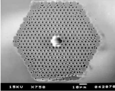
air as in standard optical fibers, but from closely spaced air holes along the fiber which, analogous to photonic crystals, form a bandgap perpendicular to the propagation direction. Figure 1.2 shows the cross section of a typi-cal photonic crystal fiber, taken from [7]. The geometry of photonic crystal
Figure 1.2: Cross section of a typical photonic crystal fiber, taken from [7].
diam-eters, but also by changing certain tubes, introducing rods, or solid cores,
changing the tube distribution or the material. Not only the mode can be confined in fibers, but also the material of the fiber can be changed to in-crease the nonlinear polarization. Gopinath et.al. used a 2cm long bismuth oxide highly nonlinear fiber to generate supercontinuum spectra with as lit-tle as 7mW average power [8]. The fiber was tapered to yield an effective area of 3.3µm2. The tapering in combination with the higher nonlinearity of the material resulted in a 400 times higher nonlinear response compared to standard silica tapered fibers. At the measured output power of 7mW the spectrum was broadened to around 300nm. Practical devices that make use of the mode confinement and material properties of optical fibers can be found, for example, in all-optical regeneration. In a silica highly nonlinear fiber2, Her et.al. [9] have shown all-optical regeneration of 40Gbit/s signals
with 3km HNLF and only 1.2W input power. In As2Se3 fibers, one of the most common chalcogenide glasses, Fu et.al. have shown similar results us-ing only 2.8m long fiber [10]. Though their input power with 8W was higher than the earlier experiment, the length of the used fiber has decreased by three orders of magnitude. This advantage can be attributed to the material properties of the fiber.
2
1.3
From fibers to microphotonics
The heat dissipation problem and speed stagnation of microprocessors in recent years necessitate the development of all-optical solutions. All optical components could serve as solutions for inter- and intra-chip communication,
or, ideally, even as optical computing units. The advantages of such schemes are the higher bandwidths per communication channel and lower, or no heat dissipation. Therefore, the ultimate goal is to develop on-chip solutions.
For this, the high mode confinement in high refractive index materials, such as silicon( with a refractive index of around 3.5) can be utilized. Silicon
also has the advantage of being the material of choice in microelectronics, hence making it easier to integrate optics with microelectronics. With such a high refractive index, single mode operation in silicon can be achieved in
photonic wires with a cross section as low as 220nm× 500nm. This is a further decrease of mode area by one order of magnitude compared to ta-pered fibers. The dimensions and fabrication processes allow us to integrate
a large number of photonic functions on a single chip. This can lead to low cost photonic integrated circuits that are superior to their electronic cousins. Many nonlinear optical effects have been demonstrated in silicon photonic
source with less than 0.45mW to demonstrate four-wave mixing at a wave-length range around 2100nm. A remarkable result for low power nonlinear optics was achieved by Espinola et.al. [12]. In a 220nm×445nm photonic wire with a length of 4.6mm, Raman amplification was demonstrated using
only20.5mW pump power and ∼1mW signal power. Degenerate four-wave mixing3 was demonstrated in dispersion engineered photonic wires with a
cross section between 550nm×300nm and 600nm×300nm with a length of 6.4mm [13]. A peak pump power of 4.2W was used in the range between
1525nm and 1540nm in order to demonstrate an on/off gain of2.9dB. This low power nonlinear operation made several low power applications possible.
Salemet.al. have demonstrated all-optical regneration using the 2R regener-ation principle according to Mamyshev [14], which will be explained in detail in chapter A.2. The regenerator consisted of an8mmlong photonic wire fol-lowed by a ring resonator filter. A saturated nonlinear transfer function was achieved with 6W maximum peak power. Salem et.al. also demonstrated signal regeneration using four-wave mixing, where only400mW were needed to saturate the nonlinear transfer function [15]. Here, the silicon photonic wire was only1.8cmlong with a cross section of300nm×500nm. While these results are already remarkable compared to the experiments in optical fibers
in terms of input power and footprint, for true integration, the footprint has
3
to be decreased even further.
1.3.1 Light localization in periodic structures
To increase the light-matter interaction further and at the same time decrease the physical dimensions of micro-optic devices, the optical path length L′
=
ngL, where ng is the group-index and L is the physical path length, can be
increased by slowing down the light pulse to a fraction of the vacuum speed of lightc= 299792458m/s.
Several techniques have been exploited to achieve slow light in matter.
The record speed of17m/swas achieved in an ultracold sodium gas by means of electromagnetically induced transparency [16]. This record speed was achieved at the expense of bandwidth by means of an atomic transition,
which resulted in a transmission peak of around 2MHz width.
For practical on-chip solutions and telecommunications, bandwidth is of key importance. Nonlinear effects such as pulse broadening or wavelength conversion rely on large bandwidths. This can be done in microphotonics
by manipulating the k-vector of a propagating wave. Structures that al-low such dispersion engineering are photonic crystal waveguides and coupled resonator optical waveguides (CROW). Both structures are resonant
Figure 1.3: Dispersion relation of a CROW with κ =−0.1, calculated using eqn 4 and an electron micrograph of a coupled resonator optical waveguide (inset, from [17]).
resonators or nanowire ring resonators or other cavity schemes. The inset of
figure 1.3 shows a CROW based on ring resonators, the most commonly used geometry, taken from [17]. A light pulse in resonance with a ring cavity can couple to a resonator and after circulating several times, it can propagate by
of the CROW [18]:
ω(k) = ω0
1−∆α
2 +κcos(KΛ)
, (4)
where ω(k) [rads ] is the angular frequency corresponding to the Bloch wave vector K [m−1
], ω0 [rad
s ] is the resonance frequency of the individual
res-onator,κ the coupling parameter4, ∆α/2the fractional self frequency shift4
and Λ [m] is the periodicity of the coupled rings. A plot of the dispersion relation can be seen in figure 1.3, calculated for ∆α/2 = 0 and κ = −0.1. By using lower absolute values for κt, the dispersion relation can be
flat-tened out and the group velocity vg =dω/dK decreased, while at the same
time the bandwidth is decreased. CROWs are a good platform for optical
buffering. In a CROW consisting of 100 ring resonators, a delay of 220ps was achieved for a footprint of0.045mm2 [17]. In comparison, in a4cmlong bent photonic wire, somewhat more than double the delay could be achieved but at the expense of a 25 times larger footprint5. On the other hand, nonlinear
optics can only be performed in CROWs to a certain extend. Since they are a resonant structure, they are bandwidth limited, but the discrete frequency comb of CROWs based on ring resonators makes parametric processes
pos-sible, and this has been studied, for example, theoretically for the case of 4
Unitless.
5
four-wave mixing [19] and second harmonic generation [20].
1.3.2 Photonic cystals as ultracompact waveguides
Analogous to conventional crystals for electrons, photonic crystals form pe-riodic potentials for electromagnetic waves. This was first investigated by Sajeev John [21] and Eli Yablonovich [22] in 1987 for light localization and
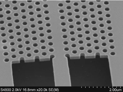
engineering of the density of states, respectively. Figure 1.4 shows an SEM micrograph of a 2D photonic crystal waveguide. The waveguide is created by removing a row of holes in the triagonal lattice of airholes in the silicon
slab. The guiding mechanism in 2D photonic crystals enable us to
engi-Figure 1.4: Electron micrograph of a 2D photonic crystal waveguide. The waveguide is formed by omitting a row of holes.
neer the dispersion with wide bandwiths of several nm. This will be subject
[image:30.595.178.375.430.578.2]harmonic generation. Typical waveguide dimensions do not extend beyond
about100µmin length and around15µmin width. One of the best examples of the advantages of photonic crystals is a5µmlong2×2directional coupler6
[23]. The coupler consists of two slow light photonic crystal waveguides that
are brought together close enough to form a supermode through which light can couple from one waveguide to the other. This compares directly to fiber optics, where several mmlong coupling sections are needed.
1.3.3 The limits of silicon and the search for other materials
Silicon microphotonics benefits from the well known material properties and the mature fabrication methods associated with the strong microelectron-ics industry. Optically, silicon has its limits in the nonlinear regime,
how-ever. On one hand, the nonlinear refractive index, (n2 ≈4.5·10−14
cmW−1
)
is very high, while on the other hand, the two-photon absorption coefficient7
(βT P A= 7.9·10 −10
cmW−1
] is also very high. Both n2 and βT P A affect the
overall phase change of an optical pulse that is travelling through a material with linear and nonlinear losses [24]:
φ =k0L+ 2π n2 βT P Aλ
·ln(1 +βT P AILef f), (5)
6
Please see appendix A.1 for the definition of a directional coupler
7
with the effective lengthLef f = (1−exp(−αL))/α[m], whereαis the linear
loss in [m−1
]. The factor
F OM = n2
βT P Aλ
, (6)
whereλ[m]is the wavelength of interest andα[m−1
]are the linear losses, can be defined as the nonlinear figure of merit. To visualize the importance of the FOM, one can look at the case of a nonlinear Mach-Zender interferometer8
made out of a material with a figure of merit of F OM = n2/βT P Aλ = 1.
A π phase shift is necessary in one arm to modulate the output signal from
high to low. This is equal to the phase change being half the wavelength
∆nL = n2IL = λ/2, where ∆n is the refractive index difference between the two arms with lengthL at wavelength λ. This phase change results in a
nonlinear attenuation of
βT P AI =
1
2L. (7)
The electric field is then attenuated by the nonlinear losses by a factor of e−1/2
:
E(L) =E0e
−βT P AI·L
=E0e
−1
2, (8)
8
whereE0 is the input electric field. This causes the output power of one arm
to decrease by e−1
:
P(L)∝ |E(L)|2 =P0e−1
, (9)
whereP0 is the power of the optical signal at the input of the interferometer. Silicon, though, has a nonlinearF OM = 0.37. Moreover, free carriers can be created successively because of the high TPA coefficient, which causes free
carrier absorption (FCA)[25]. Free carriers can be created in semiconduc-tors whose electronic bandgap is less than twice that of the incident light
energy due to two-photon absorption. This is the case for silicon, which has a bandgap of around 1100nm [26]. Moreover the silicon bandgap is indi-rect, which causes relatively long free carrier lifetimes, since they can only
relax after exchanging momentum with a phonon. In silicon, the free carrier absorption coefficient αF CA can be expressed as [27]:
αF CA = 1.45·10−29m2
λ
1.55·10−6m 2
βT P AτF CAλ
2hc , (10)
wherehis the Planck constant,cis the vacuum speed of light,τT P Ais the free
Figure 1.5: SPM broadened spectra in a slow light photonic crystal waveguide with ng ≈30, taken from [28].
SPM broadened spectra in a slow light photonic crystal waveguide (figure 1.5) is caused by the time dependence of the FCA. The pulse front creates the free carriers and the back of the pulse gets absorbed by them. Because
the lower frequency components travel in the front and the higher (blue) frequency components in the rear get attenuated. In addition to the blue side lobe being attenuated, one can also see a blue shift of the high power spectrum due to an increased refractive index caused by the free carriers.
To overcome the free carrier absorption and two-photon
ab-sorption, other nonlinear materials have to be investigated for
1.3.4 Chalcogenide glasses as a new type of nonlinear material
Chalcogenide glasses are very complex class of materials with a wealth of op-tical and structural effects. They consist of the chalcogen elements Sulphur
(S), Selenium (Se) and Tellurium (Te) or a combination of these elements together with matrix forming elements. Their refractive index ranges from n ≈ 3.5 for As2Te3 to n ≈ 2.35 for As2S3 [29]. Their most striking feature is the high nonlinear refractive index and low two-photon absorption with virtually no FCA. The fact that no FCA is observed in chalcogenide glasses at the wavelength of 1550nm is because of the bandgap energy of around Eg ≈ 2eV, which is more than double the single photon energy. They still
are within the definition of semiconductors, however. Table 1 compares the nonlinear properties of the three chalcogenide materials that are investigated
in this thesis with silicon. The three chalcogenide glasses that are investi-gated are As2S3 ,Ge33As12Se55(AMTIR-1) and Ge11.5As24Se64.5 for their high nonlinear FOMs. The highly promising nonlinear properties come at the
ex-pense of very complex structural differences from other materials. Not only is the stress modulus considerably lower than in silicon, they also have a flexible atomic structure, because the chalcogen atoms have a two-fold coordination.
differ-ent phenomena are known [30]: Photocrystallization, photopolymerization,
photodecomposition, photo-contraction and expansion, photovapourisation, photodoping and local changes in the atomic configuration. Degradation can also be seen over time. It has also been reported that chalcogenides suffer
from aging [31].
Material n2
h cm2 W i β2 cm W
FOM Bandgap[nm] Stress modulus Reference
As2S3 2·10−14 2·10−11 12.9 604 1177∼1422 N
mm2 [32] [33]
Ge33As12Se55(AMTIR-1) 15·10−14
4·10−10
2.4 600 1.17 N
mm2 [34] [35]
Ge11.5As24Se64.5 8·10−14 N/A ≈60 N/A N/A [36]
Si 4.5·10−14 7.9·10−10 0.37 1100 47·103 N
mm2 [37] [26][38] Table 1: Material comparison for the three chalcogenide glasses that are
in-vestigated in this work and silicon.
1.3.5 State-of-the-art - applications of chalcogenides and
compar-ison with silicon
Since chalcogenide glasses are amorphous compounds, different thin film9
deposition techniques were investigated for their ability to preserve the
sto-ichiometry. Pulsed laser deposition was reported for As2S3 films [39] and Ga-La-S chalcogenide thin films [40] and thermal evaporation was used to deposit Ge23Sb7S70 thin films for waveguide fabrication [41]. Several
nonlin-ear experiments were done in chalcogenide microphotonic devices. A 60mm longAs2S3 rib waveguide was used to demonstrate supercontinuum genera-tion by Lamont et.al. [42]. A 870nm high slab was etched down by 380nm
9
to form a 2µm wide waveguide. In this rib waveguide10 a 750nm wide
su-percontinuum spectrum could be achieved by pumping it with 610f s laser pulses at 68W peak power and a wavelength of 1550nm. This can be com-pared with 350nm achieved in a 4.7cm silicon nanowire using 100f s pulses [43]. By comparing the 1W input power of the silicon experiment with the
68W input power of the chalcogenide experiment, it is clear that even though the chalcogenide results are promising, the silicon results are superior. This
is due to the fact that the silicon fabrication technology is more mature. The pattern definition and etching for high quality photonic wires requires a higher level of precision than the fabrication of rib-waveguides. Rib
waveg-uides benefit from a lower field intensity at the surfaces, hence roughness and imperfections have less impact on the propagation losses. The lower inten-sity is due to the bigger mode in rib-waveguides. This affects the nonlinear
response negatively, which has to be compensated for by higher input powers.
A step towards higher mode confinement in chalcogenide glasses was the
first demonstration of photonic crystals in chalcogenide glasses that were fab-ricated by focused ion beam (FIB) milling [44] in 2005. The first photonic crystals that were fabricated using electron beam lithography and dry
etch-ing were fabricated by Yinlan et.al. in 2007 [45], avoiding the parasitic ion implantation of FIB milling. Even though, similar fabrication techniques to
10
those employed in silicon photonic crystals were used, these photonic crystals
were not coupled to access waveguides, but using the evanescent modes of a tapered silicon fiber [46]. The bandwidth limitation of this method does not allow a full characterization of the photonic crystals. The bandwidth
limitation associated with this measurement method were avoided by butt coupling that was first demonstrated in chalcogenide glasses by Suzuki et.al.
[47]. This coupling method allowed a full characterization, including
cut-off measurements, where the transition between the guided mode and the bandgap is measured. Also, the first nonlinear effects were demonstrated using this method. These photonic crystals were fabricated in silver doped
As2Se3, which caused linear losses as high as 140dB/cm [48] in the fast light regime. The four-wave mixing efficiency in these waveguides can be directly compared to the four-wave mixing results achieved in silicon [49].
Both waveguides had a similar length, with 396µm in chalcogenide glasses and 400µm in silicon. At an ng ≈ 15, Suzuki et.al. achieved a conversion
efficiency of around−14dB, whilst in silicon a conversion efficiency of−24dB was observed at an ng ≈30. Despite the higher conversion efficiency in the
silver doped chalcogenide glasses, they show three distinct drawbacks that have to be overcome: First, the high propagation losses that were partially
op-tics and, thirdly, integratability has to be demonstrated by combining the
photonic crystals with access waveguides11.
1.4
Summary
Low power, all-optical, signal processing can be performed in microphotonic devices. Photonic crystals offer a CMOS12 integrable platform for on-chip
solutions. Silicon, on the other hand, is limited in its operation due to
two-photon absorption and successive FCA. To overcome these limitations, other materials, such as chalcogenides glasses are investigated because of their higher nonlinear FOM. The results in chalcogenide photonic devices are promising, yet so far inferior to the results achieved in silicon. This is
due to the less mature fabrication technology of chalcogenide microphotonic devices. Clear advantages of chalcogenide microphotonic devices have to be
demonstrated and thus will require a higher fabrication quality.
11
Please see appendix A.1 for the definition of an access waveguide.
12
2
Dispersion Engineered Chalcogenide Photonic
Crystals
In this chapter the theory behind slow light engineering and the fabrication of slow light photonic crystal waveguides is discussed. The aim is to achieve high
group-indices away from the bandedge in order to achieve wide bandwidths over the same group-index.
2.1
Theory
2.1.1 2D photonic crystal waveguides in silicon and chalcogenides
The two-dimensional (2D) photonic crystals that are investigated in this the-sis conthe-sist of a dielectric slab withλ/2n-thickness and 2D air holes. The slab is sandwiched between air cladding for a vertically symmetric mode. A
lat-tice consisting of a triangular latlat-tice of air holes in the slab was employed. A line defect, where a row of holes is removed in the Γ−K13 direction of
the reciprocal lattice serves as waveguide. Light can propagate inside this defect, since it is confined by total internal reflection14 in vertical direction
and by the bandgap in plane. Figure 2.2 shows a schematic of a photonic crystal waveguide, where one line of holes was removed to create the line
13
Please see appendix A.1 for the definition of the reciprocal lattice and the Γ−K direction.
14
defect15. Due to their lower refractive index, 2D photonic crystal waveguides
in chalcogenide glass offer a great challenge for dispersion engineering. The relatively low refractive index contrast of nmat : nair ≈ 2.3 ∼ 2.7 : 1 results
in a narrower operative range than for silicon with a refractive index
con-trast of nmat : nair ≈ 3.48 : 1. The position of the mode within the band
diagram depends on the refractive index difference. A lower refractive index shifts the position of the fundamental mode to higher normalized frequencies
a/λ, which causes both, the k-range and wavelength range to shrink. For comparison between AMTIR-1 and silicon, figure 2.1 shows the dispersion curves for the fundamental modes of both materials with refractive indices of
3.48 and 2.6, respectively. The light line, above which the light is no longer confined by total internal reflection in the vertical direction, is indicated by the broken black line. The light grey area represents the light cone, in which
light is no longer confined due to total internal reflection but irradiates into the continuum. Due to its larger refractive index, the fundamental mode of silicon is situated lower in the bandstructure. This results in a wider k-range
between the crossing with the light-line and the end of the first Brioullin zone at k = 2π/a, where a is the lattice constant of the crystal. For silicon, this is reflected in a usable k-range of ∆k ≈ 0.44π/a. For AMTIR-1, the operative range reduces to ∆k ≈0.29π/a. This reduction in k-range affects
15
the performance of photonic crystal devices in two ways. First of all, the
operation closer to the band-edge increases the losses due to backscattering and, secondly, the k-range for dispersion engineering is reduced by a factor of about 2/3. This translates to a reduction of the usable wavelength range
down to ∆λ ≈28nm for AMTIR-1 as compared to∆λ≈87nmfor silicon.
Figure 2.1: Dispersion curve of both fundamental modes of silicon and AMTIR-1 below the light line. The light line and the bandedge limit the range of operation. The AMTIR-1 mode is shifted to higher normalized frequencies and hence is more limited in its range of operation compared to silicon.
2.1.2 Dispersion Engineering
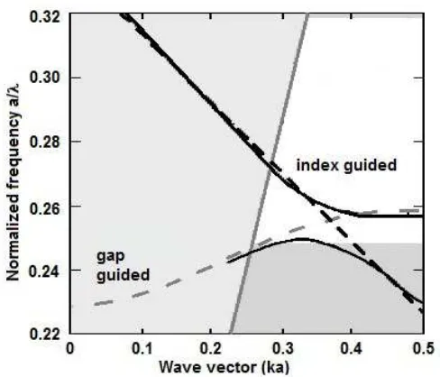
The fundamental W1 mode is a superposition of an index-guided (IG) and gap-guided mode (GG). The IG mode is confined by total internal reflection
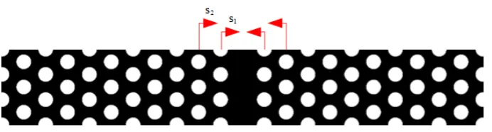
Figure 2.2: Schematic top view of a W1 photonic crystal waveguide. The shifts for dispersion engineering are marked with the red arrows s1 for the first row and s2 for the second row.
mirror, which reflects the electromagnetic wave back into the line defect. The interaction of these two modes forms the guided W1 mode [50]. At
the intersection point of the IG and GG modes the modes do not cross, but form an anti-crossing, which results in a mode gap in the photonic band gap. The position and shape of the anti-crossing can be changed by changing the
index or gap guided modes. This can be done by changing the hole radius or position of the holes adjacent to the line defect. Figure 2.3 shows the interplay between the index guided and gap guided modes that form the
W1 modes. One can see that the slope, and with it vg, decreases towards
the bandedge. But, despite the increasing ng, δλ is limited by the strong
dispersion and the bandgap. But, since it is desired to slow down light over
a wide bandwidth for nonlinear optics and signal processing, one has to take the relative bandwidth δω
Figure 2.3: Even W1 mode created by the interplay between the index guided and gap guided modes. After [50].
group-index bandwidth product
GIBP =ng
δω
ω , (11)
where the group index is defined as
ng =−
∂ω ∂k
−1
, (12)
where ω is the angular frequency and k is the wave vecotr. The GIBP can be used to compare different dispersion techniques. Several techniques have
a variation of the waveguide width, analogous of the dispersion engineering
in silicon nanowires [51]. For example, Petrov et.al. achieved an ng ≈50 by
reducing the waveguide width [52]. Notomi et.al. demonstrated experimen-tally large vg dispersion in reduced width waveguides [50]. This method has
proven to be successful in altering the dispersion properties of the waveg-uides, but at the same time, one is limited by the number of variables with which the dispersion can be controlled. Another alternative is the change
of the diameter of holes adjacent to the waveguide, which was demonstrated by Frandsen et.al. [53]. Changing the hole radius precisely is very difficult to achieve experimentally, however. Beggs et.al. have shown that a 2nm
radius change can result in a shift of 10nm in the bandedge [54]. Sufficient experimental control to achieve such precision is difficult to achieve repeat-edly. A change of the hole position longitudinally to the waveguide was used
by Hamachi et.al. [55]. An ng ≈ 50 was achieved over an experimentally
measured ∆λ ≈ 5nm, resulting in a GIBP ≈ 0.16. Li et.al. demonstrated dispersionless slow light by changing the position of the first two rows of
holes perpendicular to the waveguide [56]. Using this method a maximum GIBP ≈0.3 could be achieved, resulting in a higher∆λ at the same group-index. For example, for the same ng ≈ 50, ∆λ almost doubled to around
9nm.
applied to engineer dispersion in chalcogenide waveguides, because the high
group-index bandwidth products that were reported in silicon. The positive shift of the rows was defined to be towards the centre of the waveguide. The first row affects both the gap-guided and the index guided modes and the
second row only affects the index guided mode.
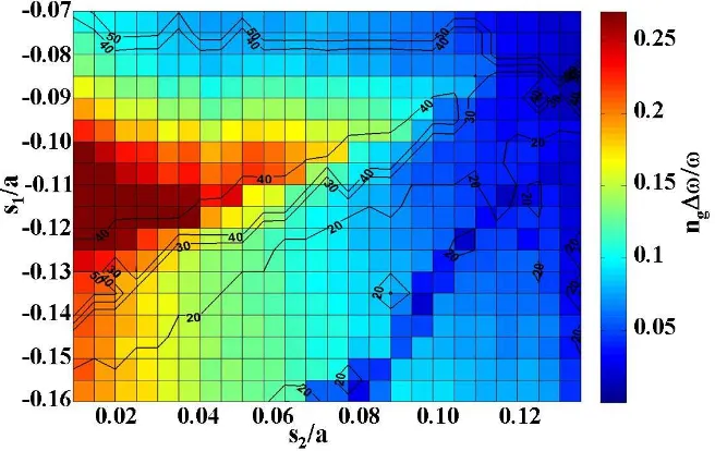
The band-diagrams were calculated using a 3D plane wave expansion
[image:46.595.117.445.416.623.2]method implemented in the ”MPB” software package [57]. The fundamental guided mode was used to calculate the group-index. The group-index was defined as being constant within a variation of ±10% The 2D color plot in
figure 2.4, shows the GIBPs for the examined parameter space for
[image:47.595.147.491.228.483.2]AMTIR-1, calculated with n = 2.6. The GIBP can be up to ≈ 0.26, whilst the ng cannot reach more than ng ≈ 40 (black countours). In AMTIR-1, an
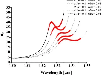
Figure 2.5: ng curves for the fundamental mode of five designs ranging from
ng ≈20 to ng ≈40. The red curves indicate the areas where ng is±10% of the mean ng.
ng ≈ 40 can be reached with ∆λ ≈ 10nm, leaving enough bandwidth for
signal processing operation. Figure 2.5 shows five ng curves versus λ. When
high ngs are reached, the ng curves are no longer flat, but show a peak,
where the dispersion changes from anomalous to normal. We also note that
the bandwidth for the four highest ng curves is almost constant to a change
2.1.3 Effects of slow light on the mode area and nonlinear
[image:48.595.183.376.195.374.2]re-sponse
Figure 2.6: Mode area calculations for differentvgs, taken from [58]
Figure 2.6 shows the intensity distribution of the electric field in W1 waveguides, taken from [58]. The field is less confined in the slow light regime than in the fast light regime. The effective mode areaAef f [m2]can
be calculated by using
Aef f =
1
a
R
V ol|E|2dV 2
R
V ol|E|4dV
. (13)
For example, the mode area in silicon photonic crystal changes from0.12µm2 to 0.5µm2 when the group-index is changed fromn
g = 4 tong = 30 [49]. In
2.1.4 Conclusions
The guiding mechanism in W1 photonic crystal waveguides allows us to mod-ify the dispersion properties of the waveguide. In this work, the first two rows
of holes adjacent to the waveguide are shifted to engineer slow light. Even though the refractive index difference in chalcogenide photonic crystals is considerably lower than in silicon, a GIBP ≈ 0.26 can be achieved. The maximum ng that can be achieved in the high GIBP regime is ≈40.
2.2
Photonic crystal fabrication
Several complicating issues occur during the fabrication of chalcogenide pho-tonic crystals:
a) They are more fragile than standard semiconductors, such as silicon or GaAs.
b) They react with basic chemicals, especially with solvents.
c) Their susceptibility to structural changes by incident light imposes fur-ther challenges in the fabrication process, such as photocrystallization
or refractive index changes.
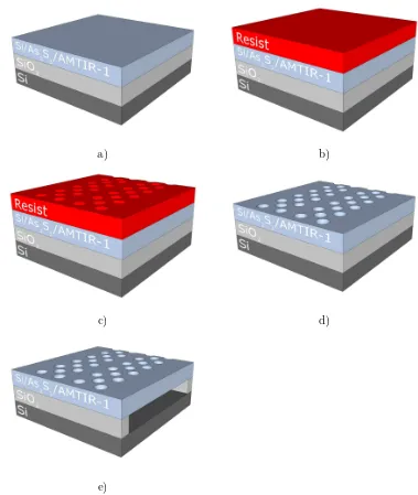
First, an overview of the fabrication process is provided, identifying the
prob-lems at each step. Next the solutions to the issues are presented and the differences with the standard silicon process are described. The process flow can be seen in figure 2.7.
2.2.1 Pre-processing
In the preprocessing, the sample is cleaved to a size of around 1×1cm2(see figure 2.7a)). The sample accumulates dust and other particles during this handling process which impede the fabrication process. Therefore the sample has to be cleaned thoroughly before further processing. This is done by
immersing the sample in a piranha solution (a 3:1 solution of sulfuric acid (H2SO4) and hydrogen peroxide (H2O2)) and successive cleaning steps in sonic bath agitated acetone (ACE) and then an isopropanol (IPA) bath. The
piranha solution oxidizes organic debris and the ACE and IPA baths remove inorganic residues with the help of sonic bath agitation. Tests that were performed using Ge33As12Se55 in the piranha solution turned out negatively
since the chalcogenide glass thin film was completely removed by the solution. Hence this solution cannot be used to clean chalcogenide glasses. To test the stability of the three chalcogenide glasses under investigation, As2S3 ,
a) b)
c) d)
[image:51.595.130.509.135.584.2]e)
microscope inspection. To test the stability of these glasses in the sonic
bath, the immersed samples were successively agitated. All samples exhibited severe damage after 10s sonic bathing at the lowest sonic bath power of 12W. Figure 2.8 shows a Ge11.5As24Se64.5 photonic crystal after a 10s sonic bath at 12W. Clearly areas of the photonic crystal are ripped away and also a micro-damage to the sidewalls can be seen in the inset of figure 2.8. This severe
Figure 2.8: Damage to Ge11.5As24Se64.5 photonic crystals due to sonic bath.
Areas are ripped away and the sidewalls are severely damaged.
damage ruled sonic bath agitation out for sample cleaning. A solution was found in the form of using a constant flow of nitrogen gas through the solvent
in which the sample is immersed. A single use HDPE pipe is placed over a conventional nitrogen gun to prevent cross-contamination. The nitrogen flow is adjusted manually. This way the solvent is stirred slowly and the bubbles
2.2.2 Chemical sensitivity
In addition to the piranha solution, IPA and ACE, further solvents are used during the fabrication steps. Xylene is used as developer of ZEON ZEP
520A electron beam resist, which is conventionally removed by either oxygen plasma etching or immersion in trichloroethylene and sonic bath agitation. MF-319 is used as developer for Shipley S1818 photo-resist. The sample was
exposed to these chemicals in order to assess the chemical durability of the chalcogenide glasses. The tests were performed in two time series. First, samples were exposed for 12 hours, and then examined using optical and
electron microscopy, and then for 24 hours with subsequent examination. Since the exposure times during the fabrication processes are much lower, these time series yield an upper limit for the expected damage. Xylene did
Process As2S3 AMTIR-1 Ge11.5As24Se64.5
Xylene Yes Yes Yes
Trichloroethylene (Tric) No No No Dimethylformamide (DMF) No Yes Yes
MF319 No No No
Sonic bath No No No
UV / O2-plasma No No No
HF gaseous gaseous gaseous
Table 2: Suitability of different chemicals and process for the chalcogenides As2S3 , AMTIR-1 and Ge11.5As24Se64.5. ”Yes” = Suitable for
chalco-genide processing, no damage observed. ”No” = Unsuitable for chalcogenide processing, damage was observed. The HF process is only possible in the gaseous phase.
hour immersion. This result enabled use of the high resolution electron-beam
resist ZEP-520A to define the photonic crystals.
Commonly, either oxygen plasma or a sonic bath in trichloroethylene is used to remove the electron beam resist after the plasma etching. In this
case, oxygen plasma was ruled out because of its reaction with chalcogenide glasses and the blue light emission during the etching which can cause light induced changed in the chalcogenide thin film. The three chalcogenide glasses
were immersed in trichloroethylene, where damage could be observed after 12 hours immersion and hence was ruled out for use as a solvent. The lack of available solvents for the resist removal was resolved by developing a new
removal method and introducing dimethylformamide as solvent. This organic solvent did not provoke any observable damage to the thin films after 24 hours of immersion and was rated as suitable for resist removal. As a last
solvent, MF-319 was tested. MF-319 is used as a developer for Shipley S1818 photo resist. Even after an immersion time of45s, severe damage to the thin film could be observed, as can be seen in figure 2.9. This ruled S1818 out
as masking material. The first method that was developed to remove the electron-beam resist involved heated Xylene. Since it is also used to develop ZEP, an artificial overdevelopment was created by immersing the photonic
crystal samples in138◦
Figure 2.9: Surface of AMTIR-1 after being exposed to MF319 for 45s. The dark spots and uneven surface suggest surface damage.
Dimethylformamide (DMF) was found to partially dissolve the electron-beam resist after immersing the sample in it for at least 6 hours. It reacts with As2S3, but the other chalcogenide glasses are stable for 48 hours. After
6 hours, the resist was removed using nitrogen bubbling. The resist does not dissolve in DMF, but it can be removed in a similar way to metal in a lift-off
process, it comes off in sheets. Unwanted redeposition has to be prevented by constant nitrogen flow when taking the sample out of the solution.
2.2.3 Light induced changes
During the processing, the samples are exposed to daylight as well as to other sources such as ultraviolet light in the plasma etching machines. This can
Figure 2.10: Surface of As2S3 after photocrystallization. The grainy
struc-ture is a sign of crystallized areas.
chalcogenide glasses, As2S3, AMTIR-1 and Ge11.5As24Se64.5 to UV light with an intensity of ≈390µW/cm2 for 120h. As
2S3 showed the most severe reac-tion with photocrystallizareac-tion. Both, AMTIR-1 and Ge11.5As24Se64.5 exhibit light refractive index changes. Figure 2.10 shows the surface of photocrystal-lized As2S3 . The grainboundaries are potential light scattering sources and
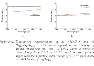
hence this material was ruled out for photonic crystal fabrication. AMTIR-1 and Ge11.5As24Se64.5 showed refractive index changes. Figure 2.11a) shows the ellipsometry measurements before and after the exposure for AMTIR-1
and b) for Ge11.5As24Se64.5 . The ∆n ≈ 0.0377 in AMTIR-1 is about 4-times higher than the∆n(≈9·10−3
a) b)
Figure 2.11: Ellipsometry measurements of a) AMTIR-1 and b)
Ge11.5As24Se64.5. After being exposed to an intensity of
around 390µW/cm for 120h, AMTIR-1 shows a refractive index change from 2.641 to 2.6787, which is about 4-times higher than the refractive index change of 9·10−3
from 2.606 to 2.615 for Ge11.5As24Se64.5 .
2.2.4 Electron-beam resists
Two electron beam resists were tested for electron-beam writing: ZEON
ZEP-520A and Polymethyl Methacrylate (PMMA), both positive resists. These resists are favourable for the creation of holes, since in positive resists the exposed areas are removed during the development. ZEP-520A has a higher
etching resistivity than PMMA and hence the layer thickness can be reduced to around 400nm in ZEP as compared to 600nm in PMMA. Important to this work is the fact that the melting temperature of ZEP is≈135◦
C, whilst
PMMA melts at ≈ 100◦
2.2.5 Electron-beam writing
The electron beam lithography was performed on a LEO 1530 SEM/ RAITH Elphy Plus hybrid system that can create beams up toE = 30keV, resulting in a wavelength of λe = hcE ≈ 41pm, which is far below the practical
reso-lution that can be achieved using electron-beam lithography. The practical resolution is set by two parameters, namely the resist’s resolution and the
proximity error.
2.2.6 Proximity Error Correction
In electron-beam lithography, the area that is exposed by the electron beam is bigger than the scanned area. The increase in exposed area is because the electrons scatter within the material. Two main scattering mechanisms
oc-cur in the resist and sample. First, forward scattering ococ-curs within the first
500nm to 1µm of penetration depth. This mechanism is mainly responsible for the resolution limitation of a given resist. The second mechanism,
back-ward scattering of electrons, occurs for electrons that have penetrated further into the material and hence have lost more energy. The typical scattering lengths of backward scattered electrons can be several micrometers. Figure
is caused by forward scattering. At the same time, a considerable fraction of
the electrons is scattered backwards. These electrons expose fractions of the resist adjacent to the scanned area. The dose of the backward scattered
elec-Figure 2.12: Monte Carlo simulations of the electron distribution during a) 10kV and b) 20kV electron beam lithography. The forward scat-tered electrons are causing most of the exposure at 20kV. Taken from [59].
trons is not high enough to clear the electron beam resist in this area, but it has to be considered when exposing complex structures. For example, during the definition of the holes for a photonic crystal, the exposure of a single hole
affects the required doses of the adjacent holes and vice versa. Figure 2.13 illustrates this process. The schematic shows three structures that are writ-ten into electron beam resist. The structure in the middle is subject to an
[image:59.595.153.475.221.409.2]Figure 2.13: Schematic of the cross-section of a sample during electron beam exposure. The black lines represent the backscattered electrons. The exposed structure in the middle is affected by the backscat-tered electrons of both adjacent structures.
lower than the doses of the outer two structures. In photonic crystals the dose of each hole has to be adjusted depending on the geometry and position
with respect to the remaining sample. Figure 2.14a) shows a photonic crystal design before and b) after proximity error correction. The bright red holes on the outside of the photonic crystal have a relative dose of around 2, whilst
the turquoise holes close to the access waveguide have a dose of around 1.5, which is a consequence of the proximity error. As expected, the inner holes are exposed by more backscattered electrons from the adjacent holes than
a) b)
Figure 2.14: Design of a photonic crystal waveguide at the input with parts of the input taper a) before and b) after the proximity error correction. The relative dose in a) is 1 and varies from 1.5 (turquoise) to 2 (bright red) in b).
exposure dose at a given point ri can be calculated to be:
D(ri) = m X
j=1
Z
A
Dj ·
1
π(1 +η) 1
α2e
r2ij
α2 + η
β2e
rij2 β2
!
, (14)
where A is the area of the section j with dose Dj [As/cm2] and α is the
forward scattering range [m], β is the backward scattering range [m] and η is the ratio of the integrated proximity effect of forward scattered electrons and backward scattered electrons. The two exponential terms give rise to the
exponential decay of the contributions of back- and forward scattering from sectionj.
con-tributions. This is used by the commercial NanoPECS package by RAITH
that was employed for proximity error correction. To determine the relevant parameters, the ”doughnut” technique, developed by Stevens et.al. [60], was adopted. The doughnut shape consists of a ring with inner radius R1 and
[image:62.595.81.476.246.458.2]a) b)
Figure 2.15: a) Schematic of the ”doughnut” that is used to determine the correction parameters. b) Matrix of the ”doughnut”-shapes to determine the proximity error correction parameters. The cir-cles represent the cleared doughnuts for As2S3 (blue), AMTIR-1
(black) and Ge11.5As24Se64.5 (green). The clearing dose is
de-fined as the dose, at which the inner circles is cleared after ex-posure and development.
outer radius R2 as can be seen in figure 2.15a). A matrix of doughnuts is created by varying the inner radiusR1along the x-axis and the exposure dose along the y-axis. The outer radius is kept constant and much larger than
dose at which the inner area opens up and the corresponding inner radius is
recorded and the relevant parameters are determined using
D=D0 ·(1 +η)·
e
R21
α2 +ηe
R21
β2
−1
(15)
as fitting formula, where R1 [m] is the inner radius. Figure 2.16 shows the resulting experimentally determined dose curves the fitted curves. Equation
Figure 2.16: Doses at which the inner circle clears with respect to the circle radius for As2S3 (blue), Ge33As12Se55 (black) and
Ge11.5As24Se64.5 (green). The solid lines are the fit-curves that
were used to determine the proximity error parameters.
14 is used to fit the experimental data, whereD0,η,α ,β are used as fitting parameters. The resulting scattering parameters can be seen in table ??.
Material η α β
As2S3 0.175 500·10−9 m 3800·10−9m
AMTIR-1 0.35 550·10−9
m 3700·10−9
m Ge11.5As24Se64.5 0.75 520·10−9m 3850·10−9m
Table 3: Fitting parameter for the proximity error correction of As2S3 and
Ge11.5As24Se64.5 .
2.2.7 Anisotropic etching of chalcogenide glass thin films
Two techniques were investigated for anisotropic etching of chalcogenide glass thin films:
a) Reactive Ion Etching (RIE).
b) Chemically Assisted Ion Beam Etching (CAIBE).
The etching mechanisms of these two techniques are inherently distinct. RIE uses a combined physical and chemical etch by reactive ion bombardment. The reaction chamber of an RIE consists of a vacuum vessel in which two
plate-electrodes are placed so that the sample can lie on one of them. A radio frequency signal between the two electrodes is used to drive a plasma of the reactants. As initial gases, most commonly SF6, CHF3or other flour
contain-ing gases are used. To activate them, they are ionized in the plasma. The bias voltage between the two plates is fixed by the plasma power and causes the radicals to move towards the electrodes, creating a directional etch. Figure
done by a directional argon ion beam. The argon ions do not react with the
sample, but sputter the material away. As a chemical component, chlorine gas is used. The gas is fed into the chamber and onto the heated sample. The heat aids the chemical etching process. Figure 2.17b) shows a sketch of
this etching machine.
a) b)
Figure 2.17: a) Sketch of the RIE chamber. The sample is placed on the yellow table, that is used as one of the RF electrodes to couple power into the plasma. The ring over the sample is both, the gas bleed and the other electrode. b) Sketch of the CAIBE etching chamber. The pink beam represents the Argon beam down on the sample through the ring that feeds the Cl2 in the chamber.
2.2.8 Reactive Ion Etching of chalcogenide glass photonic crystals
RIE is commonly used to etch silicon, based predominantly on the following reactions [61]:
SiO2+ 4F →SiF4+O2 (16)
Si+ 4F →SiF4 (17)
Si+O2 →SiO2. (18)
The addition of CHF3 can be used for sidewall passivation under the right circumstances. CHF3 can polimerize on the sidewalls and protect the
side-walls from being etched. This leads to the desired directional etching. Figure 2.18 shows an overview of the RIE etching machine including an image of the plasma. Starting from the standard silicon recipe to etch silicon
pho-tonic crystals, a parameter scan of the accessible etching parameters, time, power, gas flow, vacuum pressure and gas combinations was done on As2S3 and AMTIR-1.
Using the RIE for etching chalcogenides was problematic. The plasma emits violet and blue light, as can be seen in figure 2.18b). This can cause
a) b)
Figure 2.18: a) Overview of the Reactive Ion Etching machine. b) Plasma in the RIE chamber. The contrast within the chamber is enhanced to show the plasma.
Figure 2.19: Cross section of an AMTIR-1 photonic crystal etched with the best RIE recipe that could be achieved.
of the cross section of the best AMTIR-1 photonic crystal prepared in the RIE. The photonic crystal was etched using gasflows of10sccmH2,7sccmSF6 at a pressure of4.9·10−2
the etching.
2.2.9 Chemically Ion Beam Etching of chalcogenide glass photonic
[image:68.595.178.377.298.448.2]crystals
Figure 2.20 shows the CAIBE system that is used for the photonic crystal fabrication. A parameter scan was performed by changing the sample
tem-Figure 2.20: Chemically assisted ion beam etching machine. The big vessel is the reaction chamber, next to it the load lock system and the control electronics.
perature, the chlorine and argon flow, the ion beam current and voltage and etching time in order to determine the ideal etching conditions for all three chalcogenide glasses. Several critical parameters for etching chalcogenides
were identified:
a) The sample temperature: It is necessary to heat the sample up to
a certain temperature to aid the chemical etching process employing chlorine gas. Initially, the sample was heated toT = 125◦
a temperature of 135◦
C a reflow of the electron beam resist was
ob-served, which caused a pattern deformation that can be seen in figure 2.21. The SEM top view reveals that the resist melts and can reflow towards the middle of the sample. This causes a destructive hole size
change during the etching process. Additionally, a heat induced re-fractive index change during the etching time was suspected, which can not be prevented but was limited as far as possible. The problem
was solved by decreasing the temperature by 10◦
C and adjusting the physical etching parameters accordingly. Precise control of the heating procedure could not be achieved since the temperature was controlled
manually and, therefore, refractive index changes were suspected be-tween different etching runs.
Figure 2.21: SEM top view of an AMTIR-1 sample that was exposed to tem-peratures above 135◦
b) The ion beam source: The CAIBE is designed for deep etching of hard
materials such as GaAs. Therefore the ion beam source is designed for high beam currents at high voltages. Since chalcogenide glasses are a comparably softer material, the ion beam gun had to be driven
at considerably lower beam currents and voltages. The beam current drifted between IB = 6.5mA and IB = 8.5mA from etch to etch and
sometimes during an etch. The effect of the high beam current can be
seen in figure 2.22. The SEM micrograph reveals a filament formation at the sidewall of a Ge11.5As24Se64.5 photonic crystal sample etched with a beam current ofIB = 8.5mA. This increased sidewall roughness
destroyed the optical properties and hence the sample.
Figure 2.22: Fibre formation in a Ge11.5As24Se64.5 photonic crystal that was
Despite these problems, vertical sidewalls could be achieved for all three
chalcogenide materials under investigation. Table 4 lists the recipes for As2S3 , Ge33As12Se55and Ge11.5As24Se64.5photonic crystals. Figure 2.23 shows cross sections of the best results for a) As2S3 and b) Ge33As12Se55. The instability
Material Ar flow sccm Cl2 flow sccm t [s] IB [mA] T [◦C]
As2S3 10 3.25 2.5 6 125
Ge33As12Se55 5 1.9 9.5 7.5 115
Ge11.5As24Se64.5 5 1.9 5.5 7.5 115
Table 4: CAIBE etching recipes for As2S3 , Ge33As12Se55 and
Ge11.5As24Se64.5 .
of the ion gun and the temperature caused most of the fabricated samples to be unsuitable for further characterization. Overall, around 1 out of 30
samples were characterized successfully.
a) b)
Figure 2.23: a) As2S3 photonic crystal cross section. The sidewall angle is
less than 1◦
![Figure 1.3: Dispersion relation of a CROW with κ = −0.1, calculated usingeqn 4 and an electron micrograph of a coupled resonator opticalwaveguide (inset, from [17]).](https://thumb-us.123doks.com/thumbv2/123dok_us/8707245.382477/28.595.95.430.153.404/dispersion-relation-calculated-usingeqn-electron-micrograph-resonator-opticalwaveguide.webp)
![Figure 2.6: Mode area calculations for different vgs, taken from [58]](https://thumb-us.123doks.com/thumbv2/123dok_us/8707245.382477/48.595.183.376.195.374/figure-mode-area-calculations-dierent-vgs-taken.webp)