Abstract—This paper describes how the power efficiency of
fully integrated Dickson charge pumps in advanced smart power technologies can be improved considerably by implementing charge recycling techniques and the replacement of normal PN junction diodes by pulse-driven active diodes. These 2 methods are first analyzed and compared on a purely theoretical basis and are verified with experimental data afterwards. Measurements reveal that the combination of the 2 methods can boost the power efficiency by a factor of 2 compared to traditional Dickson charge pump designs.
Index Terms—Charge recycling, Dickson charge pump,
high-voltage generator, power efficiency optimization, smart power technology.
I. INTRODUCTION
Fully integrated charge pumps are used in a wide variety of applications, going from flash memories to dedicated display drivers. Some applications ask for specific features, such as high current drive capability or a very good output voltage stability, but for all of them a good overall power efficiency is of the utmost importance.
Achieving high power efficiency in fully integrated Dickson charge pumps is not straightforward due to the fact that integrated capacitors exhibit considerable parasitic capacitance to the substrate, resulting in a dramatic efficiency drop. In this paper charge recycling techniques are presented to substantially reduce this negative effect. Replacing the standard PN junction diodes by pulse-driven DMOS transistors acting as almost ideal active diodes is another method to enhance the power efficiency. In this paper, both methods are described theoretically and verified experimentally.
II. BASIC DICKSON CHARGE PUMP DESIGN
The basic configuration of a Dickson charge pump [1] is shown in Fig. 1. It consists of a large number of identical stages, each containing a diode and a capacitor, where the bottom plates of the capacitors in consecutive stages are driven by 2 complementary clock signals. Charge is transferred from one capacitor to the next at the rhythm of the clock, yielding an output voltage that can be much higher
Manuscript received July 5, 2010.
Jan Doutreloigne is with the Centre for Microsystems Technology (CMST), affiliated to the Interuniversity Microelectronics Centre (IMEC) and the University of Gent, Technologiepark 914A, 9052 Zwijnaarde, Belgium (phone: +32-(0)9-264-53-56; fax: +32-(0)9-264-53-74; e-mail: [email protected]).
than the input voltage. In a real application, a feedback control loop is added to the circuit in order to maintain the output voltage very stable and independent of system parameters or load characteristics. This can be achieved by continuously adjusting the clock frequency of the charge pump.
FIGURE 1.BASIC DICKSON CHARGE PUMP.
Writing down the charge balance in each capacitor under steady-state circumstances yields the following simple expression for the output voltage Vout as a function of the output current Iout, the number of stages n, the clock frequency f and the capacitor value C: ([2], [3], [4])
C
f
out
I
n
g
V
n
out
V
(
1
)
The quantity Vg is the voltage gain per stage under zero-load conditions and is given by:
T
V
cc
V
g
V
where Vcc represents the supply voltage of the charge pump and VT the forward voltage drop or threshold voltage of a diode.
We will now illustrate the design of such a charge pump for a specific situation. Let's assume that the charge pump must be capable of boosting a 3V supply voltage up to 60V output voltage under zero-load conditions. For a 0.5V diode threshold voltage, the previous equations indicate that 23 stages are needed to reach this goal. If we further assume that the application requires that the output voltage is still at least 50V at 50µA output current at a maximum clock frequency
Fully Integrated Dickson Charge Pumps with
Optimized Power Efficiency
of e.g. 10MHz, the same equations yield a minimum 12pF capacitor in each stage.
The question now is which type of integrated capacitor we best choose. In fact, each so-called smart power technology, which is actually a high-voltage extension to a standard CMOS core process, offers several types of integrated capacitors to the chip designers. The choice of 1 particular capacitor type does not only depend on the specific capacitance per unit silicon area and the maximum operating voltage, but also on the parasitic capacitance between the bottom plate of the capacitor and the substrate of the chip, as illustrated in Fig. 2:
FIGURE 2.PRESENCE OF PARASITIC CAPACITANCE.
The parasitic capacitance Cp does not contribute to the useful operation of the circuit, but it does affect the power consumption in a negative way. Indeed, the parasitic capacitance Cp is connected directly to the output of the clock buffers, and these buffers have to charge and discharge this parasitic capacitance constantly, resulting in additional power losses inside the transistors of the clock buffers, without having any useful impact on the circuit operation. Hence, the lower the value of this parasitic capacitance, the better the power efficiency will be.
In order to illustrate what types of capacitors are available in an advanced smart power technology, we’ll consider the specific example of the 100V 0.7µm I2T technology (Intelligent Interface Technology) of ON Semiconductor. Figs. 3 to 5 show a vertical cross section of 3 different kinds of integrated capacitors in this technology. Fig. 3 depicts a capacitor between a poly-silicon layer at the top and a highly doped N+ implantation at the bottom, with a very thin dielectric in between. Fig. 4 represents a capacitor structure between 2 poly-silicon layers, with a somewhat thicker dielectric. Finally, Fig. 5 shows a sandwich structure where the shorted poly-silicon and metal2 layers form 2 capacitors in parallel towards the metal1 layer. The dielectric in this structure is considerably thicker than in the 2 previous cases.
FIGURE 3.POLY-N+ CAPACITOR (PN CAPACITOR).
FIGURE 4.POLY1-POLY2 CAPACITOR (PP CAPACITOR).
FIGURE 5.METAL1-METAL2-POLY CAPACITOR (MM CAPACITOR).
Depending on the thickness of the dielectric, these capacitor types have different values of the specific capacitance per unit silicon area and maximum operating voltage, but also the parasitic capacitance towards the substrate behaves differently. These data are gathered in Table I. Apparently, the PN capacitor has the highest specific capacitance per unit silicon area because of the thinnest dielectric, but at the same time also the lowest maximum operating voltage. At the other extreme, the MM capacitor has the highest maximum operating voltage at the expense of the lowest specific capacitance per unit silicon area. The PP capacitor is settled somewhere in between. Regarding the parasitic capacitance towards the substrate, the PP capacitor is undoubtedly the best option, and the MM capacitor clearly the worst.
Capacitor type
Max. voltage
(V)
Specific capacitance
(fF/µm2)
Parasitic capacitance
(fF/µm2)
PN 12 0,75 0,27 (36%)
PP 30 0,345 0,079 (23%)
MM 100 0,091 0,057 (63%)
TABLE I.COMPARISON OF DIFFERENT CAPACITOR TYPES.
In the next 8 stages, where the operating voltage is within the range from 12V to 30V, the PP capacitor is selected. Finally, for the 11 last stages with operating voltages in excess of 30V, the MM capacitor is the only remaining option. The very bad corresponding parasitic capacitance towards the substrate is something we have to live with!
In order to assess the power efficiency of the charge pump, we first have to calculate the average current delivered by the supply voltage Vcc. This average supply current is given by the following expression:
cc
V
C
f
n
out
I
n
tot
in
I
(
1
)
,
The first term represents the average current the clock buffers have to supply to the bottom plates of the capacitors in each stage in order to compensate the charge loss caused by the output current drawn by the load. The second term represents the current delivered by the clock buffers to constantly charge the parasitic capacitance Cp in each stage. The parameter α is the ratio of the parasitic capacitance Cp to the nominal capacitor value C:
C
p
C
/
The power efficiency can then be calculated by evaluating the following equation:
tot
in
I
cc
V
out
I
out
V
,
If the number of charge pump stages n is large enough, meaning that n + 1 n, the expression for the power efficiency becomes:
out
I
cc
V
C
f
cc
V
C
f
out
I
cc
V
T
V
1
1
With an average α value of 0.444 (weighed average over the 23 stages with different capacitor types), a power efficiency of 17% is obtained at 50µA output current.
III. CHARGE RECYCLING
The reported 17% power efficiency is of course rather disappointing and is to a large extent due to the influence of the parasitic capacitance Cp. However, this effect can partly be eliminated by employing the dedicated charge recycling technique of Fig. 6:
FIGURE 6.CHARGE RECYCLING PRINCIPLE.
In this configuration, the normal clock buffers are replaced by 3-state buffer circuits. Before switching the clock buffers from one state to the next (from 0V to Vcc, or vice versa), their outputs are disabled (high-impedance output) during a very short time interval and the buffer outputs are short-circuited by means of an additional MOSFET. As a result, half of the charge that was stored on the parasitic capacitance Cp of a particular stage will be transferred to the parasitic capacitance of the next stage. Consequently, this parasitic capacitance of the next stage does not have to be charged anymore from 0V to Vcc when its clock buffer is again enabled, but only from Vcc/2 to Vcc. This technique yields a 50% reduction of the clock buffer power consumption that is related to the parasitic capacitance in each stage. This effect is clearly visible in the following expression of the average supply current where the factor ½ in the second term evidences this 50% power consumption reduction:
cc
V
C
f
n
out
I
n
tot
in
I
2
1
)
1
(
,
The very same factor ½ also appears in the expression of the power efficiency of course:
out
I
cc
V
C
f
cc
V
C
f
out
I
cc
V
T
V
2
1
1
1
output current becomes 28%, which is already substantially higher than the earlier 17% without charge recycling!
IV. PULSE-DRIVEN ACTIVE DIODES
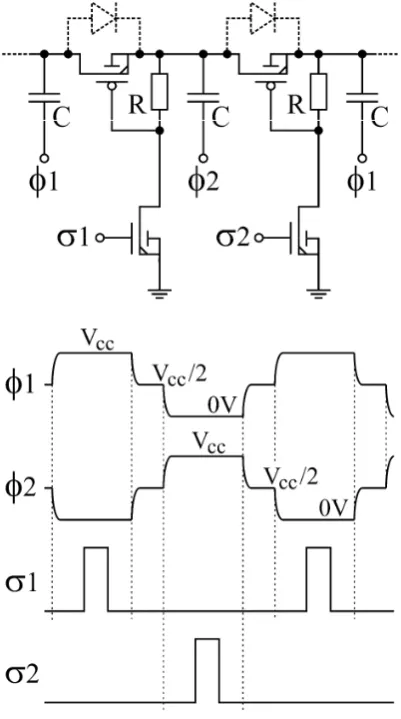
Looking at the presence of the diode threshold voltage VT in the numerator of the expression for the charge pump power efficiency, it is clear that the efficiency can be improved by lowering the VT value. A first possibility would be to replace the standard PN junction diodes by Schottky diodes that exhibit a much lower threshold voltage. Unfortunately, high-performance Schottky diodes are not readily available in most smart power technologies. An interesting alternative is to replace the diodes by properly driven transistors that provide a low-resistance path during the charge transfer between capacitors of consecutive stages. In the ideal situation, the charge transfer can be completed to its full extent during the conduction time of the transistor, meaning that the equivalent VT value in the power efficiency expression would simply be 0V, resulting in maximum power efficiency! An additional advantage is that the voltage gain per stage under zero-load conditions becomes Vcc instead of the earlier Vcc – VT, and consequently, fewer stages (and less silicon area) are needed to reach a predetermined output voltage. A possible practical implementation of this active diode approach is shown in Fig. 7:
FIGURE 7.PULSE-DRIVEN ACTIVE DIODES.
The main charge transfer transistors are actually P-type high-voltage DMOS devices, whose drain potential must be
able to go down to -2Vcc with respect to their source, and whose N-type bulk region must be able to float up to Vout with respect to the system ground. In the proposed configuration the built-in drain-bulk diodes of the P-type DMOS transistors are oriented in exactly the same way as the diodes in the original Dickson charge pump. The operation of the circuit is fairly straightforward. When the clock signal 1 goes high and 2 goes low, there will be some charge transfer from the 1-driven capacitor to the 2-driven capacitor through the built-in drain-bulk diode of the P-type DMOS transistor between them, but this charge transfer will not be complete due to the threshold voltage of the diode. But then the pulse 1 is applied to the gate of an auxiliary N-type DMOS device, being the driving transistor in a level-shifter circuit, producing a voltage drop of a few volts across resistor R, thereby activating the P-type DMOS transistor. Hence, the low-resistance channel of this device causes the charge transfer to continue until the top plates of the 2 capacitors reach exactly the same electric potential. This corresponds to the ideal situation of VT = 0V, meaning that the P-type DMOS transistors act like almost ideal active diodes. The effect of this technique is clearly illustrated in the simulation result of Fig. 8, where Vcap1 and Vcap2 are the electric potentials of the capacitor top plates in consecutive stages. The reduction of the 0.5V voltage drop (the VT of the built-in drain-bulk diode) to 0V when the P-type DMOS device is activated by the 1 pulse is very clear in this simulation. Also note the previously described charge recycling in the clock signals.
FIGURE 8.SIMULATION OF THE PULSE-DRIVEN ACTIVE DIODES.
[image:4.595.67.268.382.742.2] [image:4.595.324.533.409.728.2]not straightforward at all. Let’s have a look at the expression for the output voltage of the charge pump:
C
t
LS
I
n
n
C
f
out
I
n
cc
V
n
out
V
)
1
(
2
1
)
1
(
Apart from the fact that the voltage gain per stage under zero-load conditions is now Vcc instead of Vcc – VT , one can see that a third term has shown up in this expression. Each time a P-type DMOS transistor is activated, the level-shifter, consisting of the auxiliary N-type DMOS transistor and the resistor R, will draw a current ILS during a time interval Δt from the capacitor node. This amount of charge drawn from the stage capacitor will reduce the voltage gain of the stage. Moreover, a more detailed analysis shows that the clock buffer of a particular stage has to deliver not only the level-shifter charge ILS.Δt of that very same stage but also the level-shifter charge of all subsequent stages. This means that the voltage gain deteriorates from the output node of the charge pump towards the input node. This effect results in the n2
-dependence of the third term in the Vout expression. The same phenomenon is of course also present in the equation for the total average supply current:
t
LS
I
f
n
n
cc
V
C
f
n
out
I
n
tot
in
I
)
2
(
)
1
(
2
1
2
1
)
1
(
,
Also here a third term with a n2-dependence is visible. When calculating the power efficiency, one finds the following formula:
out
I
t
LS
I
f
n
out
I
cc
V
C
f
cc
V
C
t
LS
I
n
cc
V
C
f
out
I
2
1
2
1
1
2
1
1
The presence of the 2 n-dependent terms in this formula (with a minus sign in the numerator and with a plus sign in the denominator) proves that the level-shifter charge ILS.Δt can cause serious problems in very long charge pumps, and hence, the value of ILS.Δt should be kept small enough in order not to deteriorate the output voltage and power efficiency. Of course, the value of ILS.Δt cannot be chosen arbitrarily small: Δt should be long enough so that the charge transfer through the active diode can be completed within this time interval, and ILS should be large enough in order to produce a sufficient voltage drop across resistor R so that the active diode is effectively turned on. One could increase the value of R to allow smaller values of ILS, but this has a negative influence on the response time of the level-shifter, and the time interval Δt must then be increased accordingly. Replacing the resistor R by a non-linear active load relaxes
this issue to some extent, but current and speed can never be completely disconnected from each other. Anyway, it is clear from this analysis that the choice of the ILS.Δt product is a very critical trade-off between different requirements.
Whereas 23 stages were necessary to reach 60V under zero-load conditions with standard PN diodes, the increased voltage gain of the active diode approach requires only 19 stages to reach the same output voltage. With a level-shifter current ILS of 2µA and a time interval Δt of 10ns, the charge pump can deliver 50µA output current at 52V output voltage and 10MHz maximum clock frequency. The corresponding power efficiency is 34% when combining the pulse-driven active diode technique and the charge recycling technique. This is 6% higher than the charge recycling version with standard PN diodes.
V. THEORETICAL COMPARISON
Based on the formulas from the previous sections, Fig. 9 summarizes the theoretical Vout vs. Iout characteristics for the following parameters: Vcc = 3V, f = 10MHz, C = 12pF and average value of α = 0.444 for all charge pump versions; VT = 0.5V and n = 23 for the versions with standard PN diodes; n = 19, ILS = 2µA and Δt = 10ns for the versions with active diodes.
FIGURE 9.THEORETICAL COMPARISON OF THE VOUT VS.IOUT
CHARACTERISTICS.
All versions produce the required 60V output voltage under zero-load conditions, but the output voltage of the versions with active diodes is slightly less dependent on the output current because of the smaller number of stages.
FIGURE 10.THEORETICAL COMPARISON OF THE EFFICIENCY VS.IOUT
CHARACTERISTICS.
From Fig. 10, the importance of the proposed efficiency boosting techniques becomes very clear. Combining the charge recycling feature and the pulse-driven active diode technique almost doubles the power efficiency compared to the traditional Dickson charge pump configuration, and this over the whole useful output current range.
VI. EXPERIMENTAL DATA
[image:6.595.74.265.48.253.2]In order to verify the theoretical analysis, several charge pumps were designed and fabricated in the 100V 0.7µm I2T technology of ON Semiconductor. They all use 12pF capacitors (divided among the PN, PP and MM types as discussed before), and the versions with standard PN diodes employ 23 stages, while the active diode versions consist of 19 stages. During the experiments, the clock frequency is set to its maximum value of 10MHz, and the other system parameters are set to exactly the same values as for the theoretical comparison in the previous section: Vcc = 3V, ILS = 2µA and Δt = 10ns.
Fig. 11 depicts the measured Vout vs. Iout characteristics of the different charge pumps. A first observation is that the output voltage under zero-load conditions does not reach the targeted 60V as in the theoretical calculations of Fig. 9, but only slightly more than 50V. This discrepancy is due to the presence of additional parasitic capacitance in the charge pump stages that was not taken into account during the theoretical calculations. Indeed, there is also a parasitic capacitance between the top plates of the capacitors and the substrate, caused by the reverse-biased PN junctions between the N-type cathode regions of the PN diodes and the P-type substrate (or between the N-type bulk regions of the P-type active diodes and the P-type substrate). This voltage-dependent junction capacitance strongly affects the charge transfer between capacitors from consecutive stages, resulting in reduced voltage gain per stage. From Fig. 11 we also learn that above 60µA the output voltage has a steeper current-dependency than predicted by the formulas (note that the current scale goes up to 100µA in Fig. 11, while it goes up to 200µA in Fig. 9). This is probably caused by the fact that at
high current levels the residual voltage drop across the output transistors inside the clock buffers at the end of each half clock period cannot be neglected anymore, resulting in reduced effective switching amplitude of the clock signals. This produces of course less voltage gain per stage. Finally, from Fig. 11 it is also clear that the active diode approach has a better performance than the standard PN diode configuration, in accordance with the theoretical predictions.
FIGURE 11.EXPERIMENTAL COMPARISON OF THE VOUT VS.IOUT
CHARACTERISTICS.
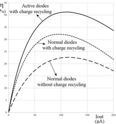
The most important experimental information is gathered in Fig. 12, showing the measured power efficiency as a function of the output current for the different charge pump versions. Comparing these experimental data to the theoretical results from Fig. 10, we learn that the maximum power efficiency is reached at an output current level of about 60µA instead of about 100µA according to the theoretical formulas, and above all, that the experimental peak power efficiency is roughly a factor 2 lower than the theoretically predicted value. There are basically 3 main reasons for this discrepancy between measurements and calculations:
[image:6.595.330.523.157.357.2] [image:6.595.329.522.554.761.2]CHARACTERISTICS.
Firstly, there is the previously mentioned effect of the additional parasitic capacitance between the top plates of the capacitors and the substrate, caused by the reverse-biased PN junctions between the N-type cathode regions of the PN diodes and the P-type substrate (or between the N-type bulk regions of the P-type active diodes and the P-type substrate). This does not only negatively influence the voltage gain per stage, but it also has a negative impact on power efficiency since the clock buffers have to supply extra current in order to continuously charge and discharge this parasitic capacitance. Secondly, as stated before, at high output current levels the effective switching amplitude of the clock signals at the output of the clock buffers is strongly reduced, resulting in much more power being dissipated inside the output transistors of the clock buffers than being transferred to the charge pump stages. Obviously, this has a negative impact on power efficiency.
Finally, there is also a lot of extra power dissipation inside the clock buffers due to the fact that the clock buffers on the real chip consist of several cascaded CMOS inverters with increasing transistor channel widths in order to ensure proper operation at high clock frequency. Of course, the parasitic gate-source and gate-drain capacitances of all transistors inside these clock buffers have to be charged and discharged at the rhythm of the high clock frequency, and this gives rise to considerable extra dynamic losses inside these circuits.
Although there is this quantitative discrepancy between experimental and theoretical data, the main qualitative conclusion from the theoretical predictions appears to remain valid after experimental verification: both the adoption of charge recycling techniques and the use of pulse-driven active diodes boost the power efficiency significantly. When combining both methods, the power efficiency is almost doubled compared to a traditional Dickson charge pump configuration!
Both power efficiency boosting techniques were successfully implemented in a bi-stable display driver for smart-card applications, using Dickson charge pumps for the high-voltage generation. The driver chip, shown in Fig. 13 and 36mm2 in size, was processed using the 100V 0.7µm I2T technology from ON Semiconductor.
FIGURE 13.DIE PHOTOGRAPH OF A PROTOTYPE DISPLAY DRIVER WITH
6 FULLY INTEGRATED DICKSON CHARGE PUMPS.
The display driver contains 2 programmable charge pumps capable of output voltages up to 55V at a 50µA load current, and 4 programmable charge pumps capable of output voltages up to 30V at a 50µA load current. These 6 programmable high-voltage generators are clearly identified in the die photograph of Fig. 13.
VII. CONCLUSION
Two methods for increasing the power efficiency of fully integrated Dickson charge pumps were presented and analyzed in this paper: the use of charge recycling techniques and the replacement of standard PN junction diodes by pulse-driven active diodes. Experimental data provide a qualitative confirmation of the theoretically predicted impact of both methods. Measurements reveal that the power efficiency is almost doubled compared to traditional Dickson charge pump configurations. The presented techniques have already been successfully implemented in a real bi-stable display driver.
REFERENCES
[1] J. F. Dickson, “On-chip high-voltage generation in MNOS integrated circuits using an improved voltage multiplier technique,” IEEE Journal
of Solid-State Circuits, Vol. 11, No. 3, 1976, pp. 374-378.
[2] G. Di Cataldo, and G. Palumbo, “Design of an n-th order Dickson voltage multiplier,” IEEE Transactions on Circuits and Systems-I:
Fundamental Theory and Applications, Vol. 43, No. 5, 1996, pp.
414-417.
[3] G. Palumbo, D. Pappalardo, and M. Giabotti, “Charge-pump circuits: power-consumption optimization,” IEEE Transactions on Circuits and
Systems I: Fundamental Theory and Applications, Vol. 49, No. 11,
2002, pp. 1535-1542.
[4] G. Palumbo, D. Pappalardo, and M. Giabotti, “Modeling and minimization of power consumption in charge pump circuits,” Proc. of the 2001 IEEE International Symposium on Circuits and Systems