For your convenience Apress has placed some of the front
matter material after the index. Please use the Bookmarks
Contents at a Glance
About the Author ����������������������������������������������������������������������������������������������������������������
xv
About the Technical Reviewer ������������������������������������������������������������������������������������������
xvii
Acknowledgments �������������������������������������������������������������������������������������������������������������
xix
Introduction �����������������������������������������������������������������������������������������������������������������������
xxi
Part 1: Hardware Foundation: Intel Xeon Phi Architecture
■
���������������������������
1
Chapter 1: Introduction to Xeon Phi Architecture
■
�������������������������������������������������������������
3
Chapter 2: Programming Xeon Phi
■
����������������������������������������������������������������������������������
15
Chapter 3: Xeon Phi Vector Architecture and Instruction Set
■
�����������������������������������������
31
Chapter 4: Xeon Phi Core Microarchitecture
■
�������������������������������������������������������������������
49
Chapter 5: Xeon Phi Cache and Memory Subsystem
■
������������������������������������������������������
�65
Chapter 6: Xeon Phi PCIe Bus Data Transfer and Power Management
■
����������������������������
81
Part 2: Software Foundation: Intel Xeon Phi System Software and Tools
■
���������
95
Chapter 7: Xeon Phi System Software
■
����������������������������������������������������������������������������
�97
Chapter 8: Xeon Phi Application Development Tools
■
�����������������������������������������������������
113
Part 3: Applications: Technical Computing Software Development
■
on Intel Xeon Phi ��������������������������������������������������������������������������������������
137
Chapter 9: Xeon Phi Application Design and Implementation Considerations
■
��������������
139
Chapter 10: Application Performance Tuning on Xeon Phi
■ Contents at a GlanCe
Chapter 11: Algorithm and Data Structures for Xeon Phi
■
����������������������������������������������
171
Chapter 12: Xeon Phi Application Development on Windows OS
■
����������������������������������
185
Appendix A: OpenCL on Xeon Phi
■
����������������������������������������������������������������������������������
195
Appendix B: Virtual Shared Memory Programming on Xeon Phi
■
�����������������������������������
199
Introduction
This book provides a comprehensive introduction to Intel Xeon Phi architecture and the tools necessary for software engineers and scientists to develop optimized code for systems using Intel Xeon Phi coprocessors. It presents the in-depth knowledge of the Xeon Phi coprocessor architecture that developers need to have to utilize the power of Xeon Phi. My book presupposes prior knowledge of modern cache-based processor architecture, but it begins with a review of the general architectural history, concepts, and nomenclature that I assume my readers bring.
Because this book is intended for practitioners rather than theoreticians, I have filled it with code examples chosen to illuminate features of Xeon Phi architecture in the light of code optimization. The book is divided into three parts corresponding to the areas engineers and scientists need to know to develop and optimize code on Xeon Phi for high-performance technical computing:
Part 1—“Hardware Foundation: Intel Xeon Phi Architecture”—sketches the salient features of modern cache-based architecture with reference to some of the history behind the development of Xeon Phi architecture that I was personally engaged in. It then walks the reader through the functional details of Xeon Phi architecture, using code samples to disclose the performance metrics and behavioral characteristics of the processor.
Part 2—“Software Foundation: Intel Xeon Phi System Software and Tools”—describes the system software and tools necessary to build and run applications on the Xeon Phi system. I drill into the details of the software layers involved in coordinating communication and computations between the host processor and a Xeon Phi coprocessor.
Part 3—“Applications: Technical Computing Software Development on Intel Xeon Phi”—discusses the characteristics of algorithms and data structures that are well tuned for the Xeon Phi coprocessor. I use C-like pseudo-algorithms to illustrate most instructively the various kinds of algorithms that are optimized for the Xeon Phi coprocessor. Although this final part of the book makes no pretensions to being comprehensive, it is rich with practical pointers for developing and optimizing your own code on the Xeon Phi coprocessor.
Part 1
Chapter 1
Introduction to Xeon Phi Architecture
Technical computing can be defined as the application of mathematical and computational principles to solve engineering and scientific problems. It has become an integral part of the research and development of new technologies in modern civilization. It is universally relied upon in all sectors of industry and all disciplines of academia for such disparate tasks as prototyping new products, forecasting weather, enhancing geosciences exploration, performing financial modeling, and simulating car crashes and the propagation of electromagnetic field from mobile phones.
Computer technology has made substantial progress over the past couple of decades by introducing superscalar processors with pipelined vector architecture. We have also seen the rise of parallel processing in the lowest
computational segment, such as handheld devices. Today one can buy as much computational power as earlier supercomputers for less than a thousand dollars.
Current computational power still is not enough, however, for the type of research needed to push the edge of understanding of the physical and analytical processes addressed by technical computing applications. Massively parallel processors such as the Intel Xeon Phi product family have been developed to increase the computational power to remove these research barriers. Careful design of algorithm and data structures is needed to exploit the Intel Many Integrated Core (MIC) architecture of coprocessors capable of providing teraflops (trillions of mathematical operations per second) of double-precision floating-point performance. This book provides an in-depth look at the Intel Xeon Phi coprocessor architecture and the corresponding parallel data structure and algorithms used in the various technical computing applications for which it is suitable. It also examines the source code-level optimizations that can be performed to exploit features of the processor.
Processor microarchitecture describes the arrangements and relationship between different components to perform the computation. With the advent of semiconductor technologies, hardware companies were able to put many processing cores on a die and interconnect them intelligently to allow massive computing power in the modern range of teraflops of double-precision arithmetic. This type of computing power was achieved first by the supercomputer Accelerated Strategic Computing Initiative (ASCI) Red in the not-so-distant past in 1996.
Chapter 1 ■ IntroduCtIon to Xeon phI arChIteCture
History of Intel Xeon Phi Development
Intel Xeon Phi started its gestation in 2004 when Intel processor architecture teams began looking for a solution to reduce the power consumption of the Intel Xeon family of processors developed around 2001. We ultimately determined in 2010 that the simple low-frequency Intel MIC architecture with appropriate software support would be able to produce better performance and watt efficiency. This solution required a new microarchitectural design. The question was: Could we use the x86 cores for it? The answer was yes, because the instruction set architecture (ISA) needed for x86 compatibility dictates a small percentage of power consumption, whereas the hardware implementation and circuit complexity drive most of the power dissipation in a general-purpose processor.
The architecture team experimented on a simulator with various architecture features—removing out-of-order execution, hardware multithreading, long vectors, and so forth—to develop a new architecture that could be applied to throughput-oriented workloads. A graphics workload fits throughput-oriented work nicely, as many threads can work in parallel to compute the final solution.
The design team focused on the in-order core, x86 ISA, a smaller pipeline, and wider single instruction multiple data (SIMD) and symmetric multithreading (SMT) units. So they started with Pentium 5 cores connected through a ring interface and added fixed-function units such as a texture sampler to help with graphics. The design goal was to create architecture with the proper balance between chip-level multiprocessing with thread and data-level parallelism. A simulator was used to anticipate various performance bottlenecks and tune the core and uncore designs (discussed in the next section).
In addition to understanding the use of such technology in graphics, Intel also recognized that scientific and engineering applications that are highly compute-intensive and thread- and process-scalable can benefit from manycore architecture. During this time period the high-performance computing (HPC) industry also started playing around with using graphics cards for general-purpose computation. It was obvious that there was promise to such technology.
Working with some folks at Intel Labs in 2009, I was able to demonstrate theoretically to our management and executive team that one could make some key computational kernels that would speed up quite a bit with such a low-frequency, highly-parallel architecture, such that overall application performance would improve even in a coprocessor model. This demonstration resulted in the funding of the project that led to Intel Xeon Phi development. The first work had started in 2005 on Larrabee 1 (Figure 1-1) as a graphics processor. The work proceeded in 2010 as a proof-of-concept prototype HPC coprocessor project code-named Knights Ferry. The visual computing product team within Intel started developing software for technical computing applications. Although the hardware did not change, their early drivers were based on graphics software needs and catered to graphics application programming interface (API) needs, which were mainly Windows-based at that point.
Core + Coherent Cache Core + Coherent Cache Core + Coherent Cache Core + Coherent Cache Core + Coherent Cache Core + Coherent Cache Core + Coherent Cache
Ring Bus Interconnects
Core + Coherent Cache F i x e d M e m o r y + I / O i / f F u n c t i o n s
Chapter 1 ■ IntroduCtIon to Xeon phI arChIteCture
The first thing the software architects recognized was that a lot of technical and scientific computing is done on the Linux platform. So the first step was to create software support for Linux. We also needed to develop a programming language that could leverage the existing skills of the software developers to create multithreaded applications using Message Passing Interface (MPI) and OpenMP with the C, C++, and Fortran languages. The Intel compiler team went to the drawing board to define language extensions that would allow users to write applications that could run on coprocessors and host at the same time, leveraging the compute power of both. Other Intel teams went back to the design board to make tools and libraries—such as cluster tools (MPI), Debugger, Amplifier XE, Math Kernel Library, and Numeric—to support the new coprocessor architecture.
As the hardware consisted of x86 cores, the device driver team ported a modular microkernel that was based on standard Linux kernel source. The goal of the first phase of development was to prove and hash out the usability of the tools and language extensions that Intel was making. The goal was to come out with a hardware and software solution that could fill the needs of technical computing applications. The hardware roadmap included a new hardware architecture code-named Knights Corner (KNC) which could provide 1 teraflop of double-precision performance with the reliability and power management features required by such computations. This hardware was later marketed as Intel
®
Xeon Phi™
—the subject of this book.Evolution from Von Neumann Architecture to Cache
Subsystem Architecture
There are various functional units in modern-day computer architecture that need to be carefully designed and developed to achieve target power and performance. The center of these functional units is a generic programmable processor that works in combination with other components such as memory, peripherals, and other coprocessors to perform its tasks. It is important to understand the basic computer architecture to get the grasp of Intel Xeon Phi architecture, since in essence the latter is a specialized architecture with many of the components used in designing a modern parallel computer.
Basic computer architecture is known as Von Neumann architecture. In this fundamental design, the processor is responsible for arithmetic and logic operations and gets its data and instructions from the memory (Figure 1-2). It fetches instructions from memory pointed to by an instruction pointer and executes the instruction. If the instruction needs data, it collects the data from the memory location pointed to by instruction and executes on them.
Interconnect
Processor Memory
Figure 1-2. Von Neumann architecture
Over the past few decades, computer architecture has evolved from this basic Von Neumann architecture to accommodate physical necessities such as the need for faster data access to implement cache subsystems. Depending on the computational tasks at hand, demands are increasingly made upon various other elements of computer architecture. This book’s focus is on Xeon Phi architecture in the context of scientific computing.
Chapter 1 ■ IntroduCtIon to Xeon phI arChIteCture
General computer architecture with a cache subsystem is designed to reduce the memory bandwidth/latency bottleneck encountered in the Von Neumann architecture. A cache memory is a high-speed memory with low latency and a high-bandwidth connection to the core to supply data to instructions executing in the core. A subset of data currently being worked on by a computer program is saved in the cache to speed up instruction execution based on generally observed temporal and spatial locality of data accessed by computer programs. The general architecture of such a computer (Figure 1-3) entails the addition of a cache to the processor core and its communication through a memory controller (MC) with the main memory. The MC on modern chips is often fabricated on a die to reduce the memory access latency.
Processor Cache MC Memory
Interconnect
Uncore Core
Figure 1-3. Computer architecture with cache memory. The memory controller is responsible for managing data movement to and from the processor
One common cache architecture design progression is to introduce and vary multiple levels of caches between the core and the main memory to reduce the access latency and interconnect bandwidth. Cache design continues to evolve in tandem with processor technology to mitigate memory bottlenecks. New memory technologies and semiconductor processes are allowing processor designers to play with various cache configurations as the architecture evolves.
The cache subsystem plays an extremely important role in application performance on a given computer architecture. In addition, the introduction of cache to speed-up applications causes a cache coherency problem in a manycore system. This problem results from the fact that the data updated in the cache may not reflect the data in the memory for the same variable. The coherency problem gets even more complex when the processor implements a multilevel cache.
There are various protocols designed to ensure that the data in the cache of each core of a multicore processor remain consistent when they are modified to maintain application correctness. One such protocol implemented in Intel Xeon Phi is described in Chapter 5.
During the development of the cache subsystem, the computer architecture remained inherently single-threaded from the hardware perspective, although clever time-sharing processes developed and supported in the computer operating systems gave the users the illusion of multiple processes being run by the computer simultaneously. I will explain in subsequent sections in this chapter how each of the components of the basic computer architecture shown in Figure 1-3—memory, interconnect, cache, and processor cores—has evolved in functionality to achieve the current version of Xeon Phi coprocessor architecture.
Improvements in the Core and Memory
To improve the single-threaded performance of programs, computer architects started looking at various mechanisms to reduce the amount of time it takes to execute each instruction, increase instruction throughput, and perform more work per instruction. These developments are described in this section.
Instruction-Level Parallelism
Chapter 1 ■ IntroduCtIon to Xeon phI arChIteCture
The instructions executed in a processor core go through several stages as they flow through logic circuits in sync with core clock pulses. At each clock pulse a part of the instruction is executed. It is possible, however, to stagger multiple instructions so that the various stages of multiple instructions can be executed in the same cycle. This is the principle behind pipelined executions.
All computer instructions based on Von Neumann architecture go through certain high-level basic stages. The first stage performs instruction fetches (IF), by which the next instruction to be executed by the core is accessed. The instructions usually reside in the instruction cache or are fetched from the main memory and cache hierarchy at this stage. Note that each stage will take a minimum of one cycle but may extend to further cycles if it gets blocked on some resource issue. For example, if the instructions to be executed are not in the cache, they have to be fetched from memory and, in the worst case, from a nonvolatile storage area such as a hard disk, solid state disk, or even flash memory.
Once the instructions have been fetched, they have to be decoded to understand how to execute the instructions. Now the instructions usually work on some sort of data, which might be in a processor register (the fastest memory nearest to the core), in a cache, or in a memory location. The semantics of the instructions are well defined by a set of rules and a behavioral model—namely, the instruction set architecture.1
A decoded instruction next moves to the execution (E) stage, where all necessary memory or cache access happens. The execution completes when all the necessary data are available. Otherwise, a pipeline stall might happen while waiting for data to come from the memory. Once the E stage completes, the data are written back (WB) to the memory/register or flags are updated to change the processor state.
Instruction Pipelining
The execution stage itself may take multiple cycles to accommodate the complexity of the semantics of that instruction. The fundamental pipelining described in the preceding section is shown in Figure 1-4. Note that this is a very simplified representation compared with the complex execution stages for the Xeon Phi processor that will be described in this book. Nonetheless, today’s complex execution stages recapitulate the high-level classical instruction stages shown in Figure 1-4.
IF ID EX M WB
Figure 1-4. Pipeline stages for an instruction execution. IF = instruction fetch; ID = instruction decode; EX = instruction execution; M = memory fetch; WB = write back, whereby the output of the instruction execution is written back to main memory
Figure 1-5 shows how the pipelining process helps the respective stages of two different instructions to overlap, thus providing instruction-level parallelism. In this figure, the first instruction (inst1), after being fetched from memory, enters the instruction-decodes stage. Since these stages are executed in different hardware components, the second instruction fetch can happen while the first instruction is in the decode stage. So in clock (clk) tick 2, the first instruction is decoded and the second instruction is fetched, thus overlapping the execution of two instructions.
1How ISAs affect the overall performance and productivity of software systems developed for particular lines of computer hardware
Chapter 1 ■ IntroduCtIon to Xeon phI arChIteCture
Processor engineers were, however, looking for more parallelism to satisfy the demand of computer users wanting to execute faster and more complex applications on these pieces of hardware. To further improve processor architecture, the architects designed the cores such that they could execute multiple instructions in parallel in the same cycle. In this case, some of the hardware functions were replicated so that, in addition to the pipelining shown in Figure 1-5, two independent instructions could be executed in two different pipelines. Thus they could both be in the execution stage at the same clock cycle. This architecture is known as superscalar architecture. One such architecture which was in wide use in early 1990s was Intel P5 architecture. The Intel Xeon Phi core is based on such architecture and contains two independent pipelines arbitrarily known as the U and V pipelines. Chapter 4 details how instructions are dispatched to these two pipelines, as well as some of the limitations of superscalar architecture.
Engineers kept increasing processor execution speed by increasing core clock frequencies. Increased clock rate required, however, that each of the stages described above be broken into several substages to be able to execute with each clock tick. Eventually the number of stages increased from the five basic stages shown in Figure 1-5 to over 30 stages to accommodate faster processor clock rate.2 This increase resulted in faster and faster processors that could execute a single thread of instructions at a speed that was improving with clock rate improvement in each subsequent processor generation. The Intel Pentium 4 processors could run at 3.7GHz at 90nm technology during the 2004 launch date.3 Given the technology limitations of that time, this was a great achievement.
But progress hit the “power wall”: the increased clock rate was resulting in too much wasted energy in the form of heat. So engineers went back to the design board. Intel Xeon Phi instructions go through fewer stages (5 stages for best case execution) than the Pentium 4 families of processors (20 stages for the best case).
Another way to improve instruction-level parallelism was through the introduction of out-of-order instruction processing. In general the processor executes the code in the order generated by the compiler based on the source code provided by the programmer. If the instructions are independent in the instruction stream that is fed to the processor, however, it is possible to execute the instructions out of order—that is, the instruction that comes later in the compiler-generated code may be executed earlier than the instruction before it in the same code stream.
In out-of-order instruction execution, the hardware can detect independent instructions and execute them in any order that speeds up the instruction execution. This meant that the order of the instructions given in the source code by the programmer was not maintained by the execution unit. This was all right from the program-correctness perspective, since the instructions were executed in parallel or even earlier than the following instruction in the program order, independently of each other. This feat was achieved by increasing resources in the various stages of the processor—primarily in the dispatch and execution units of the pipeline. The processor was able to execute them out of order and, in many cases, in speculative fashion. For example, if there were a branch in the code stream, the processor could go ahead and execute both sides of the branch even though one of the branches were later thrown out, as that branch did not meet the actual branch criterion when it reached that point. To maintain the consistency semantics of program execution, which requires that the processor state should be in the order that the programmer desired in the original code, the WB stage was nevertheless maintained in the program order.
IF ID
IF
EX
ID EX
M WB
M WB
1 2 3 4 5
inst1
inst2
clk
Figure 1-5. Instruction pipeline showing two instructions executing at the same clock cycle but at different stages
2Intel Pentium 4 Processors with Netburst Architecture (Codenamed Prescott) had a 31-stage pipeline
(http://people.apache.org/~xli/presentations/history_Intel_CPU.pdf).
3http://ark.intel.com/products/27492/Pentium-4-Processor-Extreme-Edition-supporting-HT-Technology-
Chapter 1 ■ IntroduCtIon to Xeon phI arChIteCture
Single Instruction Multiple Data
In order to increase parallelization within the hardware, the architects implemented a new hardware that allows you to work on multiple data items in parallel with a single instruction. Suppose, for example, that you have image-processing software in which you want to increase the brightness of every pixel by a certain amount. The computation involves working on consecutive bytes of data to be incremented by a certain value. Before the introduction of the single instruction multiple data (SIMD) feature, the hardware had to read one byte at a time and add the constant and write the data back. With the introduction of the SIMD unit, also commonly dubbed the vector unit, the hardware can now work on many bytes in the same cycle by one instruction.
As you will learn in Chapter 3, the vector unit in Intel Xeon Phi can work on 16 single-precision floating point values at the same time. This provided a big performance gain in applications that are data-parallel—meaning that the dataset being processed by the application has no dependencies among the data and can be processed at the same time.
Multithreading
As processor frequency was coming down to reduce the power dissipation resulting from high-speed switching, the engineers turned to hardware multithreading to increase parallelism. In this strategy, many processor resources are replicated in hardware, so that applications can indicate to the operating system that it can execute multiple instruction streams in parallel through high-level parallelism constructs such as OpenMP and Posix thread.
To the operating system, this looked like multiple processors working together to achieve the performance it wants. In the Intel Xeon Phi processor, there are four hardware threads sharing the same core as though there were four processors connected to a shared cache subsystem. Figure 1-6 shows the multithreading support in the core is displayed as logical processors, as they still share some resources among themselves.
LP0 LP1 LP2 LP3
Cache
Mutithreaded Processor
MC Interconnect Memory
Figure 1-6. Multithreaded processor cores with superscalar execution units. LP0–3 in the diagram indicate logical processors. MC indicates the memory controller controlling data flow to or from the logical processors
Multicore and Manycore Architecture
Chapter 1 ■ IntroduCtIon to Xeon phI arChIteCture
The evolution to manycore architecture allowed applications to improve performance without increasing the clock frequencies. But this advance shifted the burden of achieving application performance improvement from hardware engineers toward software engineers. Software engineers and computer scientists leveraged years of experience in developing parallel applications used in technical computing and HPC applications to start exploiting the manycore architecture. Although the parallel constructs to exploit such machines are still in their infancy, there are sufficient tools to start developing for these machines. Figure 1-7 shows the initial thinking on architectures in which more than one core is made part of a processor, such that the processor cores P0–Pn are connected to a common interconnect known as a bus through the cache subsystem (C) and share the bus bandwidth with each other.
P0 C
C P1
Pn C
MC
Interconnect Memory
Figure 1-7. Architecture evolving toward a manycore processor-based computer. C = cache; MC = memory controller; Px = processor cores
Interconnect and Cache Improvements
In using multiple cores to create a processor, it was soon discovered that single shared-interconnect architectures, such as the bus used in some early processor designs, were a bottleneck for extracting parallel application performance.
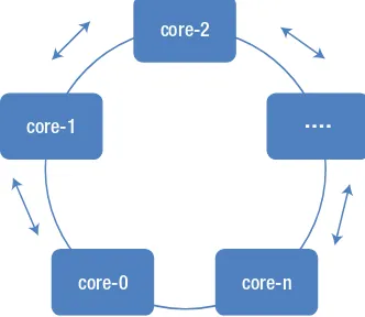
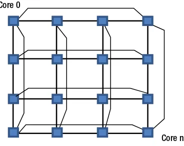
The interconnect topology selected for a manycore processor is determined by the latency, bandwidth, and cost of implementing such technology. The interconnect technology chosen for Intel Xeon Phi is a bidirectional ring topology. Here all the cores talk to one another through a bidirectional interconnect. The cores also access the data and code residing in the main memory through the interconnect ring connecting the cores to memory controller. Chapter 5 examines the interconnect technology implemented in Xeon Phi. As new designs come out, the interconnect technology will also evolve to provide a low-latency/high-bandwidth network.
Chapter 1 ■ IntroduCtIon to Xeon phI arChIteCture
System Interconnect
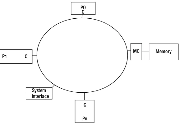
In addition to talking to memory through memory interconnects, coprocessors such as Intel Xeon Phi are also often placed on Peripheral Component Interconnect Express (PCIe) slots to work with the host processors, such as Intel Xeon processors. This is done by incorporating a system interface logic that can support a standard input/output (I/O) protocol such as PCIe to communicate with the host. In Figure 1-8, the system interface controller is shown as another box connected to the ring.
Figure 1-9 shows a system-level view of Xeon Phi coprocessor working with a host processor over a PCIe interface. Note that the data movement between the host memory and Xeon Phi memory can happen through direct memory access (DMA) without host processor intervention in certain cases, which will be covered in Chapter 6. It is possible to connect multiple Intel Xeon Phi cards to the host system to increase computational power.
P1 C
System interface
C
MC Memory
PO C
Pn
Figure 1-8. Manycore processor architecture with cores connected through a ring bus. P0–Pn = cores; C = cache; MC = memory controller
Intel Xeon
Processor Intel ProcessorXeon Phi PCI Express Gen2
Figure 1-9. System with the Intel Xeon Phi coprocessor
Chapter 1 ■ IntroduCtIon to Xeon phI arChIteCture
Intel Xeon Phi Coprocessor Chip Architecture
This section describes the various functional components of the Intel Xeon Phi coprocessor and explains why they are designed the way they are.
Figure 1-11 is a simple diagram of the logical layout of some of the critical chip components of the Intel Xeon Phi coprocessor architecture, which include the following:
• coprocessor cores: These are based on P54c (Intel Pentium from 1995) cores with major modifications including Intel 64 ISA, 4-way SMT, new vector instructions, and increased cache sizes.4
• VPU: The vector processing units are part of the core and capable of performing 512-bit vector operations on 16 single-precision or 8 double-precision floating-point arithmetic operations as well as integer operations.
• L2 Cache: The L2 cache and uncore interface.
• tag directories (TD): Components used to look up cache data distributed among the cores. • ring interconnect: The interconnect between the cores and the rest of the coprocessor’s
components—memory controllers, PCI interface chip, and so on.
• memory controller (MC): Interface between the ring and the graphics double data rate (GDDR) memory. • PCIe interface: To connect with PCIe bus.
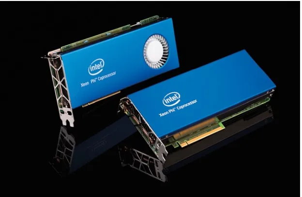
Figure 1-10. Intel Xeon Phi coprocessors in actively-cooled and passively-cooled versions. (Source: http://newsroom.intel.com/docs/DOC-3126#multimedia)
4Various other features in the coprocessor such as the debug features required to validate and debug the hardware will not be covered
Chapter 1 ■ IntroduCtIon to Xeon phI arChIteCture
Intel Xeon Phi consists of up to 61 Intel-architecture cores. For so many cores and functional units to access and communicate with each other, carefully designed interconnects are needed to hold the memory/data/control traffic between the cores and various parts of the chip. Figure 1-11 shows the logical layout of the Intel Xeon Phi coprocessor; the actual physical layout of the individual functional units may be vastly different from the depiction in the figure. For example, the eight memory controllers represented as “distributed 8x MC” in the figure are physically distributed on the ring for optimal memory access latency. The L2 caches are fully coherent with each other. Coherency is maintained by the globally owned and locally shared (GOALS) coherency protocols, described in Chapter 5. The functional units communicate with one another by on-die bidirectional interconnects.
For eight memory controllers with two GDDR5 channels running at 5.5 GT/s, one can compute the theoretical memory bandwidth as follows:
aggregate memory bandwidth = 8 memory controllers × 2 channels × 5.5 (GT/s) × 4 (bytes/transfer) = 352 GB/s
The system interface of the chip supports PCIe2 × 16 protocols with 256-byte packets.
The chip also provides reliability features useful in a technical computing environment. These include parity support in the L1 cache, error correction code (ECC) on L2 and memory transactions, cyclic redundancy code (CRC), and command-address parity on the memory I/O. Chapter 6 will provide further details on these.
Applicability of the Intel Xeon Phi Coprocessor
As seen in the preceding section, Xeon Phi is a manycore processor with up to 61 cores, with each core capable of performing 512-bit vector operations per cycle. The coprocessor card can also host up to 16GB of high-bandwidth memory. The card is, however, in a PCIe card form factor and must incur some overhead transferring data from the host processor or other nodes in a cluster. Another issue is that the cores of Xeon Phi run at about a third the speed of Intel Xeon processors, causing computations to be single-threaded. Hence the question customers often face: In which situations does it make sense to employ the Xeon Phi coprocessor-based model?
Chapter 1 ■ IntroduCtIon to Xeon phI arChIteCture
The card is not a replacement for the host processors. It has instead to be thought of a coprocessing element providing optimal power performance efficiency to the overall system. In order to achieve that power efficiency, the code must have certain characteristics that fit the hardware architecture, as follow:
The fragment of the code that is offloaded or running on the coprocessor must be highly •
parallel and must scale with the number of cores. In short, the code fragment must be able to make use of all the available cores without keeping them idle. As many of the serial functions of the computation should be performed on the host as possible.
The code must be efficiently vectorizable. It is not sufficient that the code simply be scalable •
to all the threads and cores in the Xeon Phi manycore coprocessor. The threads and cores must also be able to make use of the vector units efficiently. By efficient usage, I mean that the vector unit should not stall on the data, so that it can throughput at the rate Xeon Phi has been designed for.
The code should be able to hide the I/O communication latency with the host by overlapping •
the I/O with the computation whenever possible. This is necessary because the host will be responsible for most of the data input and output to the permanent data storage and for managing network traffic to other nodes in a cluster or grid.
These three power-efficiency optimization characteristics will be explored in detail in Chapter 9. In my opinion, Xeon Phi’s prime value is in providing the best power performance per node in a cluster. The chief benefit to be gained from adding Xeon Phi to your Xeon cluster of nodes is the increase in overall cluster performance resulting from improved performance per watt if you exploit Xeon Phi’s architecture and tools in accordance with the programming guidance presented in this book.
Intel Xeon Phi is an architecture designed to enable scientific and technical computing applications in areas as disparate as weather forecasting, medical sciences, energy exploration, manufacturing, financial services, and academic research. All of these technical computing domains rely on applications that are highly parallel. If such applications are deemed a proper fit for the Xeon Phi architecture and if they are programmed properly, Xeon Phi enables a much higher performance and power efficiency than is attainable by host nodes only.
Summary
This chapter reviewed the development of the Intel Xeon Phi coprocessor and examined the thinking behind the evolution of Von Neumann basic architecture into a complex manycore design embedded in the current Xeon Phi architecture. The motive force driving this evolution has been the quest for the ever higher levels of processor performance necessary for executing the computational tasks that today underlie scientific discoveries and new technical applications.
Chapter 2
Programming Xeon Phi
Viewing the Intel Xeon Phi as a black box, you can infer its architecture from its responses to the impulses you provide it: namely, the software instructions you execute on the coprocessor. The objective of this book is to introduce you to Intel Xeon Phi architecture in as much as it affects software performance through programming. I believe one of the best ways to understand and learn about a new architecture is to observe its behavior with respect to how it performs in relation to the requests made of it.
This chapter looks at the tools and development environment that are available to developers as they explore and develop software for this coprocessor. The knowledge in this chapter provides the foundation for writing code to evaluate various architectural features implemented on the coprocessor, which will be covered in Chapters 3 through 6.
Intel Xeon Phi Execution Models
Intel Xeon Phi cores are Pentium cores and work as coprocessors to the host processor. Pentium core adoption allowed developers to port many of the tools and much of the development environment from the Intel Xeon-based processor to the Xeon Phi coprocessor. In fact, the software designer opted for running a complete micro OS based on the Linux kernel rather than the driver-based model often used for PCIe-based attached cards, comparable to graphics cards on a system.
There are various execution models that can be used to design and execute an application on the Intel Xeon Phi coprocessor in association with the host processor. The programming models supported for the coprocessor vary between the Windows OS and Linux OS used on the host system. For example, the native programming model is only available on Linux but not on Windows. Intel Xeon Phi supports only Linux and Windows operating environments. The compiler syntax for running on the Windows environment is very close to that for the Linux environment. To simplify the presentation, I focus in this book on the Linux-based platform only.
The most common execution models can be broadly categorized as follows (Figure 2-1):
Chapter 2 ■ programming Xeon phi
Coprocessor native execution mode. An Intel Xeon Phi has a Linux micro OS running in it and can appear as another machine connected to the host, like another node in a cluster. This execution environment allows the users to view the coprocessor as another compute node. In order to run natively, an application has to be cross-compiled for the Xeon Phi operating environment. Intel Composer XE provides a simple switch to generate cross-compiled code.
Symmetric execution. In this mode the application processes run on both the host and the Intel Xeon Phi coprocessor. They usually communicate through some sort of message-passing interface such as Message Passing Interface (MPI). This execution environment treats the Xeon Phi card as another node in a cluster in a heterogeneous cluster environment.
Host Process Main()
HOST
PCI Express
Offload Compute Offload Compute
Offload Compute Model Intel Xeon Phi
Intel Xeon Phi
Intel Xoen Phi
Symmetric Compute Model
Native Compute Model
PCI Express P4
HOST
HOST Main()
F1() F2
P1 P2
P3 F1()
F2()
Figure 2-1. Intel Xeon Phi execution models. Here P indicates processes and F() indicates function calls in various execution modes. The arrows indicate the function invocation, message passing, and data communication directions between the processes and functions
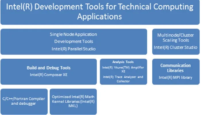
Development Tools for Intel Xeon Phi Architecture
Chapter 2 ■ programming Xeon phi
Intel Composer XE
Intel Composer XE is the key development tool and Software Development Kit (SDK) suite available for developing on Intel Xeon Phi. The suite includes C/C++ and Fortran compiler and related runtime libraries and tools such as OpenMP, threading building block, Cilk Plus, a debugging tool, and the math kernel library (MKL). Together they give you the necessary tools to build your application for Intel Xeon-compatible processors and Intel Xeon Phi coprocessors. You can also use the same compiler for cross-compilation to Intel Xeon Phi.
On the assumption that you have access to an Intel Xeon Phi–based development environment, I will walk you through how you can write a simple application to run on the various execution modes described above. Once you learn to do that, you can progress to Chapter 3 on Xeon Phi architecture to get a better understanding through experimentation.
The present chapter also covers the runtime environment and system-level details to give you a complete understanding of how the software architecture is created to work in conjunction with the host processor to complement its computations.
The C/C++/Fortran tools contained in the Intel Composer XE support various parallel programming models for Intel Xeon Phi, such as Intel Cilk Plus, Intel threading building blocks (TBB), OpenMP, and POSIX threads (pthread). The Composer XE also contains the Intel MKL, which contains common routines for technical and high-performance computing applications, including Basic Linear Algebra Subroutines (BLAS), Fast Fourier Transform (FFT), and standard interfaces for technical computing applications.
Getting the Tools
All of the toolsdescribed in this chapter for developing for Intel Xeon Phi are available from the Intel web site. If you do not have the tools, you can get an evaluation version of the tools from
Chapter 2 ■ programming Xeon phi
Using the Compilers
The C++/Fortran compilers included as part of the Intel Composer XE package generate both offload and cross-compiled code for Intel Xeon Phi. The compiler can be used in a command-line or Eclipse development environment. This book will follow the command-line options. If you are interested in the Eclipse development environment, refer to the user’s guide provided as part of the compiler documentation.
This book covers Xeon Phi-specific and -related features on 64-bit Redhat Linux 6.3 for the Intel Xeon processor. I will assume “bash” script command syntax in the examples. The compiler contains a lot of features that will not be covered in this book. The command prompt will be indicated by the ➤ symbol.
In order to invoke the compiler, you need to set some environment variables so the compiler is in the path and runtime libraries are available. To do this, you need to invoke a batch file called compilervars.sh included with the compiler. If you have installed this in the default path chosen by the compiler, the batch file to set the environment can be found at /opt/intel/composerxe/bin/compilervars.sh. To set the path invoke > source /opt/intel/ composerxe/bin/compilervars.sh intel64.
The compiler is invoked and linked with icc for building C source files and icpc for building and linking C++ source files. For Fortran sources, you need to use the ifort command for both compiler and link. Make sure you link with the appropriate command, as these commands link to the proper libraries to produce the executable.
Of course, you can use the make utility to build multiple objects. If you are porting an application built with GNU C Compiler (gcc) to Xeon Phi, you will need to change the build script to use the Intel compiler and to modify the command line switches appropriately. Because it is hard to remember all the switches, you can always invoke Intel compilers like icc with >icc -help to figure out the appropriate options for your compiler builds. In most cases, if not asked specifically for compiling only, an icc or icpc command will invoke both the compiler and the linker. In fact the commands icc, icpc, and ifort are driver programs that in turn parse the command-line arguments and processes in accordance with the compiler or the linker as necessary. The driver program processes the input file and calls the linker with the object files created, as well as the library files necessary to generate final executables or libraries. That is why it is important to use the proper compiler so that the appropriate libraries can be linked.
The Intel compiler uses file extensions to interpret the type of each input file. The file extension determines whether the file is passed to the compiler or linker. A file with .c, .cc, .CC, .cpp, or .cxx is recognized by the C/C++ compiler. A Fortran compiler recognizes .f90, .for, .f, .fpp .i90, and .ftn extensions. A Fortran compiler assumes that files with .f90 or .i90 extensions are free-form Fortran source files. The compiler assumes .f, .for, and .ftn as fixed-form Fortran files. Files with extensions .a, .so, .o, and .s are passed on to the linker. Table 2-1 describes the action by the compiler depending on the file extensions.
Table 2-1. File Extensions and Their Interpretation by the Intel Compiler
File extensions
Interpretation
Execution
.c C source file C/C++ compiler
.C, .CC, .cc, .cpp, .cxx C++ source file C++ compiler .f, .for, .ftn, .i, .fpp, .FPP, .F, .FOR, .FTN Fixed form Fortran Fortran compiler .f90, .i90, .F90 Free form Fortran Fortran compiler
.a, .so, .o Library, object files Linker
.s Assembly file assembler
The Intel compiler can be invoked as follows:
Chapter 2 ■ programming Xeon phi
where
<compiler name> is one of the compiler names such as icc, icpc, ifort;
[options] are options that are passed to the compiler and can control code generation, optimization, and output file names, type, and path.
If no [options] are specified, the compiler invokes some default options, such as –O2 for default optimization. If you want to modify the default option for compilation, you will need to modify the corresponding configuration file found in the installed <compiler install path>bin/intel64_mic or similar folders and named as icc.cfg, icpc.cfg, and so forth. Please refer to the compiler manual for details.
Compiler options play a significant role in tuning Intel MIC architecture, as you can control various aspects of code generation such as loop unrolling and prefetch generation.
You might find it useful to look at the assembly code generated by the compiler. You can use the –S option to generate the assembly file to see the assembly-coded output of the compiler.
Setting Up an Intel Xeon Phi System
I will assume you have access to a host with one or more Intel Xeon Phi cards installed in it and one of the supported Linux OSs on the host. (For Windows please refer to the corresponding user’s guide.) There are two high-level packages: the drivers (also known as the Manycore Platform Software Stack (MPSS) package) and the development tools and libraries packages (distributed as Intel Cluster Studio or a single-node version of Intel Composer XE) from which to build a system and in which you can develop applications for Intel Xeon Phi.
Install the MPSS Stack
Install the MPSS stack by the following steps:
1. Go to the Intel Developer Zone web page (http://software.intel.com/mic-developer), go to the tab Tools & Downloads, and select “Intel Many Integrated Core Architecture (Intel MIC Architecture) Platform Software Stack.” Download the appropriate version of the MPSS to match your host OS and also download the readme.txt from the same location.
2. You will need super-user privilege to install the MPSS stack.
3. Communication with the Linux micro OS running on the Intel Xeon Phi coprocessor is provided by a standard network interface. The interface uses a virtual network driver over the PCIe bus. The Intel Xeon Phi coprocessor’s Linux OS supports network access for all users using ssh keys. A valid ssh key is required for you to access the card. Most users will have it on their machine. If you have connected to the other machine from this host through ssh you most probably have it. If you do not have an ssh key, execute the following code to generate the ssh key:
user_prompt> ssh-keygen
user_prompt> sudo service mpss stop user_prompt> sudo micctrl --resetconfig user_prompt> sudo service mpss start
4. Make sure you have downloaded the correct version of the MPSS stack that matches your host operating system where you installed the Intel Xeon Phi card. If not, the MPSS source is provided to build for some of the supported Linux OS versions.
Chapter 2 ■ programming Xeon phi
6. Install the rpms in the untarred directory with an appropriate rpm install command. For example, on Red Hat Enterprise Linux you can use the following command on the command line as a root user:
command prompt> yum install --nopgpcheck --noplugins --disablerepo=* *.rpm
7. Reset the driver using:
command_prompt>micctrl -r
8. Update the system flash if necessary. To see whether you need to update, please run command_prompt>/opt/intel/mic/bin/micinfo, which will print out the Intel Xeon Phi–related information including the flash file.1
The flash files can be found in the folder /opt/intel/mic/flash and should match with those printed out as part of the micinfo. If the installed version is older than the one available with the new MPSS you are installing, update the flash with the micflash utility. Please refer to the readme.txt provided with the documentation to select the proper flash file. Once you have determined the proper flash file for the revision of the card on your system, use the following command to flash: command_prompt>/opt/intel/mic/bin/ micflash -Update /opt/intel/mic/flash/<your flash file name>
9. Once the flash is updated, reboot the machine for the new flash to take effect. The MPSS is installed as a Linux service and can be started or stopped by service mpss start|stop|restart commands.
10. Note that you need to have the proper driver configuration to get the card started. A mismatched card configuration from a previous install could prevent the card from booting. I would strongly suggest you read up on MPSS configuration and micctrl utility in the readme.txt if you encounter any issue starting the card.
Install the Development Tools
Install the Intel C/C++ compiler by obtaining the Intel Composer XE package or a superset of this package such as Intel Cluster Studio XE for Linux. Follow the instructions provided in the link in the “Install the MPSS Stack” section on how to get access to the tools and for step-by-step methods to install. Since these steps are the same as for installing the Intel tools on any Intel Xeon processor-based hosts, I am not going to cover them here.
Code Generation for Intel Xeon Phi Architecture
The traditional Intel compiler has been modified to support Intel Xeon Phi code generation. In order to do that, compiler engineers had to make changes at various levels.
The first step was adding new language features that allow you to describe the offload syntax for a code fragment that can be sent to the coprocessor. These language features are introduced by the new OpenMP 4.0 Technical Report as well as the Intel proprietary C/CFortran extensions.
1 The default MPSS install puts most of the Intel Xeon Phi–related drivers, flash, and utilities in the /opt/intel/mic and /usr/sbin
Chapter 2 ■ programming Xeon phi
Second, Intel needed some new compiler options to account for Intel MIC architecture-specific code generations and optimizations. These include providing new intrinsics corresponding to Intel Xeon Phi–specific ISA extensions, as discussed in Chapter 3. These intrinsics will help us explore various architectural features of the hardware. Finally, we need to provide support for the new environment variables and libraries to allow execution of the offload programs on the hardware.
There are two predominant programming models for Intel Xeon Phi. One is the native execution mode by which you cross-compile the code written for Intel Xeon processors and run the resulting executable on the Xeon Phi micro OS. The other is the heterogeneous or hybrid mode, by which you start the main code on the host and the code executes on the coprocessor or both the host and the coprocessor.
Native Execution Mode
Being chiefly concerned with architecture, this book mainly deals with the native execution mode, as this is the simplest way to run something on the Xeon Phi hardware. In native execution mode, you can run any C/C++/Fortran source that can be compiled for Intel Xeon or can be cross-compiled for Intel Xeon Phi architecture. The code is then transferred to the Xeon Phi coprocessor OS environment using familiar networking tools such as secure copy ( scp ) and executed in Xeon Phi’s native execution environment.
In this section I shall assume you already have access to a system with an Intel Xeon Phi coprocessor installed in it. I shall also assume you have downloaded the appropriate driver and Composer XE on your machine from the Intel registration center.
Hello World Example
Let’s try running a simple “Hello world” application on the Intel Xeon Phi processor in native mode. Say you have a simple code segment as follows in a source file test.c:
//Content of test.c #include <stdio.h> int main()
{
printf("Hello world from Intel Xeon Phi\n"); }
To build the code you need to compile and link these files with a -mmic switch as follows:
command_prompt>icc -mmic test.c -o test.out
This will create an output file test.out on the same folder as your source. Now copy the source file to the Intel Xeon Phi mic0 as follows:
command_prompt>scp test.out mic0:
This will copy the test.out file to your home directory on the coprocessor environment. At this phase you can log in to the coprocessor using the ssh command as follows:
Chapter 2 ■ programming Xeon phi
Figure 2-3. Executing a Hello world program inside Intel Xeon Phi micro OS command prompt. The printout is from the code running on a Xeon Phi coprocessor
The listing now shows the file test.out on the native coprocessor environment. If you run it on the card, it will printout:
command_prompt-mic0>./test.out
Hello world //printed from Intel Xeon Phi command_prompt-mic0>
I have also captured a screenshot of this execution, as shown in Figure 2-3.
Language Extensions to Support Offload Computation on
Intel Xeon Phi
Intel has extended the C/C++ and Fortran language to support programming the Intel Xeon Phi coprocessor. OpenMP 4.0 standard also includes extensions to target similar coprocessor computing models.
Heterogeneous Computing Model and Offload Pragmas
There are two supported ways to deal with nonshared memory between an Intel Xeon Phi coprocessor and the host processor. One is data marshaling, in which the compiler runtime generates and sends data buffers over to coprocessors by marshaling the parameters provided by the application. The second option is the virtual shared memory model, which depends on system-level runtime support to maintain data coherency between the host’s and coprocessor’s virtual shared memory address space. Because the first model is supported by OpenMP 4.0 specifications and is more prevalent than the second model, the first model will be the working model in all subsequent chapters.
The Intel compiler had proprietary language extensions that were implemented to support the nonshared programming model before the OpenMP 4.0 specifications were published.
In the nonshared virtual memory space programming model, the main program starts on the host and the data and computation can be sent to Intel Xeon Phi through offload pragmas when the data exchange between the host and the coprocessor are bitwise copyable. The bitwise copyable data structures include scalars, arrays, and structures without indirections. Since the coprocessor memory space is separate from the host memory space, the compiler runtime is in charge of copying data back and forth between the host and the coprocessor around the offload block indicated by the pragmas added to the source code.
Chapter 2 ■ programming Xeon phi
In order to provide seamless execution so the same code can run on the host processor with or without a coprocessor, the compiler runtime determines whether or not the coprocessor is present on the system. So if the coprocessor is not available or inactive during the offload call, the code fragment inside the offload code block may execute on the host as well.
Language Extensions and Execution Model
In order to understand the new language extensions for nonshared memory programming, we should understand the terminology introduced in OpenMP 4.0 specifications to describe the language support.2 The treatment of the terminology and directives in this section is not comprehensive but rather covers those parts of the specifications that are relevant to the Intel Xeon Phi offload programming model.
Terminology
device. A device may have one or more co-processors with their own memories or a host. A host device is the device executing the main thread. A target device executes the offloaded code segment.
offload. The process of sending a computation from host to target.
data environment. The variables associated with a given execution environment.
device data environment. A data environment associated with target data or a target construct. mapped variable. Either variable when a variable in a data environment is mapped to a variable in a device data environment. The original and corresponding variables may share storage.
mappable type. A valid data type for a mapped variable.
Offload Function and Data Declaration Directives
These directives are used to declare functions and variables so that these are available on the coprocessor.
declare target Directives
declare target directives declare data, functions, and subroutines that should be available in a target (coprocessor) execution environment. They allow the creation of versions of specified function or data that can be used inside a target region executing on the coprocessor.
Syntax
C/C++
#pragma omp declare target new-line declaration-definition-sequence
#pragma omp end declare target new-line
Chapter 2 ■ programming Xeon phi
Fortran
!$omp declare target (list) new-line
In C/C++/Fortran, variables and function declarations that appear between declare and end declare target or in the list argument are created in the device context and can be used or executed in the target region.
Restrictions
Threadprivate variables cannot be in a
• declare target directive.
Variables declared in a
• declare target directive must have a mappable type.
In C/C++ the variables declared in a
• declare target directive must be at file or
namespace scope.
Function Offload and Execution Constructs
In order to execute on a coprocessor, a target device must be available on the host system running the code. For the nonshared memory model, the host application executes the initial program, which spawns the master execution thread called the initial device thread. The OpenMP pragma target and pragma target data provide the capability to offload computations to a coprocessor(s).
Target Data Directive
This directive causes a new device data environment to be created and, encountering the task, executes the target data region.
Syntax
C/C++
#pragma omp target data [clause [[,] clause],...] new-line structured-block
Fortran
!$omp target [clause[[,] clause],...]
parallel-loop-construct | parallel-sections-construct !$omp end target
Where clauses are:
device(scalar-integer-expression) •
The integer expression must be a positive number to differentiate various coprocessors •
Chapter 2 ■ programming Xeon phi
map([map-type:]
• list)
These are data motion clauses that allow copying and mapping of variables or common •
block to or from the host scope to the target device scope. The map type:
• alloc indicates the data are allocated on the device and have an undefined initial value. • to declares that on entering the region, each new data in the list will be initialized to
original list item value.
• from declares that the data elements are “out” type and copied from the device data to host data on exit from the region.
• tofrom(Default) declares that data elements are in or out type and values are copied to and from the data elements in the device corresponding to data elements on the host.
If the list is an array element, it must be a contiguous region. •
if(scalar-expr) •
if the scalar-expression evaluates to false, the device is a host. •
Restrictions
At most one• device clause may appear on the directive. The device expression must evaluate to a positive integer value.
At most one
• if clause can appear on the directive.
Target Directive
This directive provides a superset of functionality and restriction of the target data directive, as discussed in the previous subsection.
A
• target region begins as a single thread of execution and executes sequentially, as if enclosed in an implicit task region, called the initial device task region.
When a
• target construct is encountered, the target region is executed by the implicit device task.
The task that encounters the
• target construct waits at the end of the construct until
execution of the region completes. If a coprocessor does not exist, is not supported by the implementation, or cannot execute the target construct, then the target region is executed by the host device.
The data environment is created at the time the construct is encountered, if needed. Whether •
a construct creates a data environment is defined in the description of the construct.
Syntax
C/C++
Chapter 2 ■ programming Xeon phi
Fortran
!$omp target [clause[[,] clause],...] structured-block
!$omp end target
where clauses are:
device(scalar-integer-expression) •
The integer expression must be a positive number to differentiate various coprocessors •
available on a host. If no device is specified, the default device is determined by the ICV named default-device-var (OMP_DEFAULT_DEVICE openmp environment variable). The default data environment is constructed from the enclosing device environment, the data environment of the enclosing task, and the data mapping clauses in the construct.
map([map-type:]
• list)
These are data motion clauses that allow copying and mapping of variables or common •
block to or from the host scope to the target device scope. The map type:
• alloc indicates the data are allocated on the device and have an undefined initial value. • to declares that on entering the region, each new data in the list will be initialized to
original list item value.
• from declares that the data elements is “out” type and copied from the device data to the host data on exit from the region.
• tofrom(Default) declares that data elements are in or out type and values are copied to and from the data elements in the device corresponding to data elements on the host.
If the list is an array element, it must be contiguous region. •
if(scalar-expr) •
if the scalar-expression evaluates to false, the device is a host. •
The target directive creates a device data environment and executes the code block on the target device. The target region binds to the enclosing structured block code region. It provides a superset of target data constructs and describes data as well as the code block to be executed on the target device. The master task waits for the coprocessor to complete the target region at the end of the constructs.
When an if clause is present and the logical expression inside the if clause evaluates to false, the target region is not executed by the device but executed on the host.
Restrictions
If a target, target update, or target data construct appears within a target region, then the •
behavior is undefined.
The result of an
• omp_set_default_device, omp_get_default_device, or omp_get_num_devices routine called within a target region is unspecified.
The effect of access to a
• threadprivate variable in a target region is unspecified.
A variable referenced in a
Chapter 2 ■ programming Xeon phi
A variable referenced in a target region but not declared in the target construct must appear in •
a declare target directive.
• C/C++ specific: A throw executed inside a target region must cause execution to resume within the same target region, and the same thread that threw the exception must catch it.
The syntax for expressing data transfers between host and coprocessors is expressed by target data and update constructs, as discussed in the next section.
Target Update Directive
Target update directive synchronizes the list items in the device data environment consistent with their corresponding original list items according to the map clause.
Syntax
C/C++
#pragma omp target update motion-clause[clause[[,] clause],...] new-line
Fortran
!$omp target update motion-clause [clause[[,] clause],...]
Where motion-clause is one of the following:
to(list) from(list)
Each list item in the to or from clause corresponds to a device item and a host list item. The from clause corresponds to out data from the device to the host and the to clause corresponds to in data from the host to the device.
Clauses are:
device(scalar-integer-expression) •
The integer expression must be a positive number to differentiate the various •
coprocessors available on a host. If no device is specified, the default device is determined by an ICV named default-device-var.
if(scalar-expr): If the scalar expression evaluates to false, the
• update clause is ignored.
Runtime Library Routines
The OpenMP 4.0 specifications also provide routines to set and get runtime environment settings (referred to as ICVs in the OpenMP specs) and to query the number of available coprocessors using the following APIs: