A Novel Hardware Efficient Reconfigurable
32-Bit Arithmetic Unit for Binary, BCD
and Floating Point Operands
MOHIT TYAGI
Electronics and Communication Department
Priyadarshini College of Computer Sciences, Greater Noida, India-201308
APURVA VASHIST
Computer science Department
Priyadarshini College of Computer Sciences, Greater Noida, India-201308
KAVITA KHARE
Electronics Department
Maulana Azad National Institute of Technology (MANIT)-Bhopal, India-462051
Abstract— This paper provides the details for novel adder/subtractor arithmetic unit that combines Binary, Binary Code Decimal (BCD) and single precision Binary floating point operations in a single structure. The unit is able to perform effective addition-subtraction operations on unsigned, sign-magnitude, and various complement representations. The design is runtime reconfigurable or can be implemented in ASIC as a runtime configurable unit and maximum utilization of hardware resource are the feature of the architecture. All the subunits have been designed to work with least delay. The modified unit and base unit were synthesized for 4vfx60ff672-12 Xilinx Virtex 4 FPGA for comparison. The proposed design has 8.9ns delay and achieve throughput of 112.3 MOPS using only 2% of the available hardware resources of the targeted FPGA. Under the assumption that significant part of the hardware in the proposed structure is shared by the different operation reconfigurable platforms with partial reconfiguration become an interesting target.
1. Introduction
Various application e.g. internet, industrial control etc require precise arithmetic for different data representation formats. Such application cannot tolerate errors of conversion between binary and decimal formats. If a binary approximation is used instead of an exact decimal fraction, result can be incorrect even if subsequent arithmetic is correct. When performing decimal operation on traditional binary based hardware, Excessive delays are introduced. Therefore, decimal arithmetic is necessary in many financial and commercial applications that process decimal values and perform decimal rounding.
Binary Floating point (FP) addition/Subtraction is the most frequent FP operation and accounts for almost half the scientific operation and thus fundamental component of math coprocessor, DSP processors, embedded arithmetic processors, and data processing units and applications, such as numerical analysis, scientific computing, and simulations. It is a costly operation in terms of hardware and timing as it needs different types of building blocks with variable latency.
But to facilitate binary, BCD and floating point applications on the same hardware a reconfigurable approach needs to be adopted. This chapter deals with the design of a single architecture that can perform arithmetic operations of three notations: binary, BCD, and single precision floating point addition/subtraction. It also supports both signed and unsigned operations for binary and BCD representation.
This single architecture is similar to presented in [10] that are capable of performing various related operations by sharing the same hardware.
2. Background for BCD arithmetic
8421 BCD is a way to express each of the decimal digits with binary code. There are only first ten 4-bit binary code groups (00002 to 10012) are used to express each decimal digit from 0 to 9. The designation 8421 BCD
code indicates binary weights of the four bit (23, 22, 21, 20). The remaining 4-bit binary code groups (10102 to
11112) for decimal digit from 10 to 15 are left unused when decimal computing is considered. Assuming two
decimal numbers are added using a 4-bit binary adder. The following steps are performing for BCD addition: 1. Add two 4-bit BCD numbers (equivalent to decimal digit) using binary addition.
2. If 4-bit sum is equal to or less then 9, the sum is valid BCD number and no correction is needed. 3. If the 4-bit sum is greater than or if a carry is generated from the sum is invalid BCD number. Then, the
digit 6 (01102) should be added to the sum to correct the invalid BCD representation.
In case of decimal subtraction, additional processing needed for 10’s complement of the subtrahend. As the BCD code do not include a code for decimal digit 10 and for this reason a nine’s complement representation is used and generate carry from the sum is again added to the sum.
2.1 Related work for binary/BCD
In this section, an overview is given for five binary and decimal adder / subtractor that have already been designed. Some of the initial contribution were designed by Schmooklar et al.[1] and Adiletta et al. [2]. Later, combined of Binary and BCD adders were designed by Levine et al.[3] and Anderson[4], while first BCD sign-magnitude adder/subtractor was designed by Grupe [5]. An area efficient sign-sign-magnitude adder was later developed by Hwang [6] as shown in fig.1. Area occupied by this design was least amongst all the previous designs.
Figure 1. Hwang’s proposal [6]
Flora [7] followed the principle of carry select adders and came up with a design which concurrently process two results, one assuming the presence of an input carry and the other assuming in its absence. Fischer et al. [8] (Fig. 2) later came up with a compact design that employed only one adder but the latency was a problem as it had to use an additional correction block.
During the last decade various BCD adder/subtractordesigns have been developed for the IBM S/390, G4, G5, G6 and eServer Z900 microprocessorsbased on the design presented by Haller et al. [9].
Thisarchitecture is shown in Fig. 3 operated in a single cycle, though requiring correction corrections in some cases. In the case of subtraction there is a need for the computation of the complement after the subtraction to obtain correct difference, hence increasing the latency. Recently, Haller et al.optimized the carry chain in the same architecture whichslightly reduced the delay but with an increased area of theunit.
Figure 3. Haller’s proposal (Z900)
The design of the Universal Adder (Fig. 4) proposed by D.R.Humberto et al. [10] uses effective addition/subtraction operations on unsigned/sign-magnitude, and various complement representations. This design overcomes the limitations of previously reported approaches that produce some of the results in complement representation when operating on sign-magnitude numbers. This design proposed that the major disadvantage of the previous designs i.e. having the subtrahend the smaller number in magnitude, was eliminated by their approach, but this design has highlatency.
Figure 4. Humberto’s Proposal [10]
Figure 5. Sreehari’s Proposal [11]
The pre-computation block consists of logic to compute propagate and generate signals for both BCD and Binary addition/subtraction.This employs a new method of subtraction unlike theexisting designs which mostly use 10’s complements, toobtain a much lower latency.
2.2 Related work for Single precision floating point
A number of attempts at constructing floating-point arithmetic in FPGAs have been done and presented in the academia. However, many of the proposals are a bit old and few targets modern FPGAs such as the Virtex-4. High-performance floating-point arithmetic on FPGAs is discussed in [13]. Although the paper has some interesting figures about the area against pipeline depth tradeoff, their design seems to be a bit to general to utilize the full potential of the FPGAs.
To be fully IEEE 754 compliant, the floating-point unit needs to support denormalised numbers, be it either with exceptions, letting a processor deal with these uncommon numbers, or having direct support for denormalised numbers in hardware. For a good discussion on different strategies to handle denormalised numbers, see [14]. Although it is a good general discussion, the chapter does not cover any FPGA-specific details.
A pipelined floating point adder based on IEEE 754 format is developed and the design is compared with that of an unpipelined floating point adder also complaint with IEEE 754 format and a rigorous analysis is done for speed, area, and power considerations [15]. The functional partitioning of the adder into four distinct stages operates simultaneously for different serial input data stream. It not only increases the speed but also is energy efficient. All these improvements are at the cost of slight increase in the chip area. Although this design perform only additions, in this chapter we used as a base.
Figure 4.1: Algorithm of Pipelined Adder/Subtracter [37]
3. Reduced Delay Universal Adder
The main objective of our design was to reduced delay of binary and BCD adder/subtrator operations using parallelizing and pipelining scheme. To achieve this we used the Humberto [10] design as a base. We kept its functionality as it is, with minimizing its delay. For unsigned and sign-magnitude addition/subtraction or effective addition/subtraction, we also use s/370 sign-magnitude adder [12] as a base.
Let us assume N1 and N2 being two n-bit sign-magnitude numbers, such that N1 = [N1n−1 N1n−2...N10] and N2 =
[N2n−1N2n−2...N20], with N1n−1 and N2n−1 used as sign bits of binary or BCD representations. The two modified
sign bits are computed as follows:
N1S = N1n−1 · Sign (1.1)
N2S = N2n−1 · Sign (1.2)
Where input Sign = 0 signal, in the case of unsigned and complement representations. Otherwise signed representation will be performed.
Consider the operation SUM= N1 Add N2, with input signal Add indicates desirable addition/subtraction and SUM being the result of the operation. The addition/subtraction operation of two unsigned-magnitude numbers decided by Add input signal (Add=0 for addition & Add=1 for subtraction), while for signed-magnitude numbers addition/subtraction operation performed by the sign bits and Add input signal. Conclusion is that the addition/subtraction of two unsigned/signed- magnitude numbers can be performed with the determination of effective operation.
Assuming the operation involves true value of the signed numbers. The effective operation can be computed by the following Boolean expression:
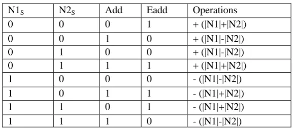
Eadd = (N1S⨁ N2S ⨁ Add) (1.3)
Table 1. Effective operations
The computation of the magnitude of the SUM can be achieved by the following. Assume that the effective addition/subtraction operation is performed on the absolute values of N1 and N2, denoted by |N1| and |N2| respectively, and assume that the operation produces no overflow.
Assume that the operation is binary effective addition. Then the following equation establishes binary effective addition:
SUM= |N1|+|N2|+ Co (1.4)
Where, Co is used to find whether |N1| is greater than |N2| or less than/equals to |N2|. Co should be equals to zero for effective addition. Boolean expression for Co can be defined as following:
Co= G0n-1 [|N1|, |N2|]
=Gn-1| (Pn-1.Gn-2)|...| (Pn-1.Pn-2…Pn-i.Gi)|…..
| (Pn-1.Pn-2……P1.G0) (1.5)
Where Gi = N1i.N2i and Pi=N1i|N2i are generate and propagate signals respectively.
Assume that the operation is binary effective subtraction and all possibilities can be defined as following: Case 1: If |N1|>|N2| then SUM will be positive and the following equation establishes binary effective subtraction:
SUM= |N1|+|N2|+ Co (1.6)
Where Co =1 because |N1|>|N2| and performs 2’s complement subtraction.
Case 2: if |N1|<|N2| then SUM will be negative and the following equations establish binary effective subtraction:
SUM= |N1|+|N2|+ Co (1.7)
Where Co=0 because |N1|<|N2| and SUM itself in one’s complement representation to represent negative SUM. Case 3: if |N1|=|N2| then sum will be zero and the following equations establish binary effective subtraction: SUM= |N1|+|N2|+ Co (1.8)
Where Co=0 because |N1|=|N2|.
In order to generate a correct sign-magnitude result, an additional correction step ⨁SC is used. The final magnitude result becomes:
|SUM|= ∑ ⨁SC (1.9) The SC is computed as follows:
SC= Co.Eadd (1.10)
N1S N2S Add Eadd Operations
0 0 0 1 + (|N1|+|N2|)
0 0 1 0 + (|N1|-|N2|)
0 1 0 0 + (|N1|-|N2|)
0 1 1 1 + (|N1|+|N2|)
1 0 0 0 - (|N1|-|N2|)
1 0 1 1 - (|N1|+|N2|)
1 1 0 1 - (|N1|+|N2|)
Finally, the sign bit of the result is updated as shown equation 1.11 [12]. SUMn-1= [N1n-1⨁(Co.Eadd)].(SUM≡0))] (1.11)
With SUM≡ 0 represents SUM equal to zero.
3.1 Decimal arithmetic addition
In this section we describe in more details of additional additions to the original binary adder needed for decimal addition/subtraction operations.
Assume that the operation is decimal effective addition. Then the following equation establishes decimal effective addition:
SUM= |N1|+|N2|+01102 + 0 (if DC=1) (1.12)
SUM= |N1|+|N2| + 0 + 0 (if DC=0) (1.13)
Assume that the operation is decimal effective subtraction and all possibilities can be defined as following: Case 1: If |N1|>|N2| then SUM will be positive and the following equation establishes decimal effective subtraction:
SUM= |N1|+|N2*|+ 01102+1 (if DC=1) (1.14)
SUM= |N1|+|N2*| + 0 + 0 (if DC=0) (1.15) Where ‘*’ indicates nine’s complement of the operand.
Case 2: if |N1|<|N2| then SUM may be negative and the following equations establish decimal effective subtraction:
SUM= |N1|+|N2*|+ 11002 + 0 (if DC=1) (1.16)
SUM= |N1|+|N2*|+01102 + 0 (if DC=0) (1.17)
Case 3: if |N1|=|N2| then sum and DC signal will be zero and the following equations establish decimal effective subtraction:
SUM= |N1|+|N2*|+01102 + 0 (1.18)
The digital carry logic (DC) [13] signal for decimal operations are obtained as follows: DC=A|B.Cin (1.19)
Where
A=G3|P3.P2|P3.P1|G2.P1 B=P3|G3|P2.G1
The final digital carry logic can be determined by the Boolean equation (1.20) which is a modified version of equation (1.19).
DC=A|B.Cin (1.20) Where
A=G3|P3.P2|P3.P1|G2.P1|P3.G0|G2.G0 B=P3|G3|P2.G1
one’s complement then “DigitWise-6” (DW) hardwired logic, as used in many previous designs [9]. The DW value ND = N2−610 is obtained with the following equations that modify each bit of the BCD nibble as follows:
ND[3] = N2[3] · N2[2]|N2[3] · N2[1]|N2[3] · N2[2] · N2[1] ND[2] = N2[2] ⨁ N2[1]
ND[1] = N2[1] ND[0] = N2[0]
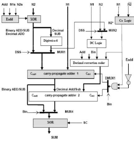
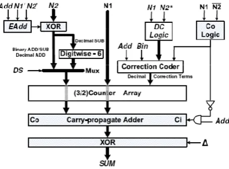
Please note that when a binary operation is performed Bin = 1 the decimal correction term is not needed and left inactive, otherwise decimal operations are performed. The reduced delay binary and BCD adder is set up with the aforementioned logic, two carry-propagate-adder, some multiplexers and de-multiplexers, and a set of XOR gates. The final organization is depicted in Figure 6. Note that the input N2* for computing the digit carry logic is equal to nine’s complement when processing decimal subtraction. When processing decimal addition N2* is equal to N2 otherwise left inactive. The multiplexer signal control for decimal subtraction or any addition (DSS) is computed by:
DSS = Eadd · Bin (1.21) The final complement operation is controlled by equation (1.10): SC= (Co · Eadd)
Figure 6.Architecture for reduced delay universal adder
The whole architecture of the reduced delay universal adder sub- divided into six subunits. Sixth subunit is Carry in circuitry for both carry-propagate-adder including Co logic works parallel to the rest design. The first subunit of our proposal includes Eadd logic, XOR and Digitwise-6 logic while second subunit includes DC logic and decimal correction coder. Third and fourth subunits are carry-propagate-adder 1 and carry-propagate-adder 2 respectively. The SUM correction SC logic divides as a fifth subunit.
Assume binary operation is performed. In order to perform binary arithmetic, only first, third, and fifth subunits works together in pipelined manner while sixth subunit works parallel to the rest units. Digitwise-6 logic, second and fourth subunits are left unused. And in order to perform decimal operation, first five subunit works together in pipelined manner while sixth subunit in parallel. Second subunit follows first subunit and fourth subunit follows third subunit.
subtrahend and output SUM and the carry in logic circuitry including Co logic) are reused in both binary and BCD operation modes.
4. Proposed algorithm for floating point arithmetic
Verilog HDL can be used to represent several different abstraction levels. The level chosen to represent the 32-bit floating-point adder includes a mixture of register-level and gate-level logic block.
Figure 4.3: Proposed algorithm for pipelined floating point adder
The following section describes how the proposed 32-bit floating-point adder uses the different types of processes (Figure 4.3) to build the pipelined adder architecture.
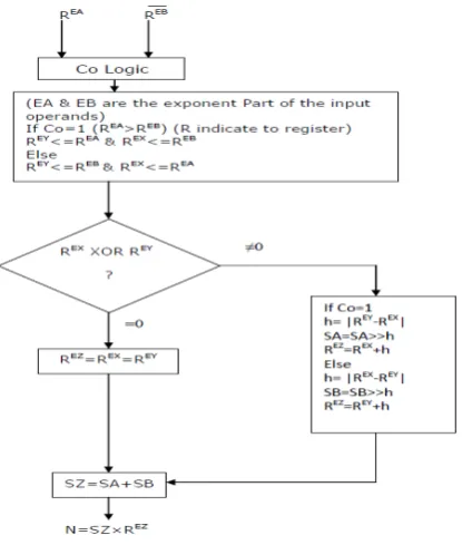
4.1 Stage 0: Comparator Stage Determining which of the two operands has the greater magnitude alleviates complex conditionals in later stages of the adder. The initial stage in the adder uses Co logic with one 8-bit XOR array instead of conventional comparator logic to place the larger of the two operands as operand A. The Boolean expression for Co logic as given below: Co is used to find whether |N1| is greater than |N2| or less than/equals to |N2|. Co should be equals to zero for effective addition. Boolean expression for Co can be defined as following:
Co= G0n-1 [|N1|, |N2|] = Gn-1| (Pn-1.Gn-2)|...| (Pn-1.Pn-2…Pn-i.Gi)|…. | (Pn-1.Pn-2……P1.G0) (3.5) Where Gi = N1i.N2i and Pi=N1i|N2i are generate and propagate signals respectively
The combinational Verilog HDL process compares the exponents to make an initial determination. If the exponents are equal, the logic then compares the mantissa values. Sign bits do not affect the comparison. The registered process handles insertion of the implied leading-one for each new mantissa value. The leading-one insertion operation always takes place regardless of the operand values. Stage 2 performs zero value exception handling.
4.2 Stage 1: Denormalization Shift Calculation Stage In order to add two floating-point values in scientific notation, the two values must have the same exponent in both sign and magnitude. The adder must perform this operation by shifting one of the operands and making adjustments to the operand exponent value. Stage 1 of the pipeline takes the difference of the two operand exponents to determine how many shifts are needed on operand B. By shifting to the right, the operand stands to lose only lower significant bits.
results occurring due to the inserted leading-one of Stage 0: Should the operands not produce a potential zero result, the rest of Stage 2 performs the shifting operation on operand B using a barrel shifter. The adder examines the shift value obtained by taking the difference of the exponents in Stage 1. Upon leaving the stage, the adder only needs to keep a single exponent and sign bit along with the two mantissas.
4.4 Stage 3: Mantissa Addition/Subtraction Stage Stage 3 of the adder pipeline performs the addition/subtraction of the two mantissa integer values. The sign bit indicates whether addition or subtraction takes place and if the carry-in bit to the adder/subtractor should be a 0 or 1, respectively. Performing subtraction requires a 2’s-complement addition and adding in a 1 for the carry-in bit. In order to reduce extra cycle to add carry out bit in 2’s complement addition to perform subtraction, the output of Co logic used as carry-in bit for carry-propagate adder. Note that since operand A is greater than operand B, a borrow bit cannot happen, and thus, the carry-out bit of the result is cleared.
4.5 Stage 4: Addition Carry-Out Exception Handling Stage The resulting mantissa value must always go through the leading-one detection (LOD) logic regardless of the carry-out bit. If the pipeline stage determines a subtraction took place or if an addition took place with no carry-out, no changes to the mantissa have to be done. But if an addition took place with a carry-out, an immediate adjustment to the exponent must be done prior to the LOD stage since the bit does not take part in the 23-bit mantissa result vector. To do so, the stage must shift the result vector to the right by one to accommodate the carry-out bit as the new leading-one. The LOD logic will then find the leading-one in bit location 23.
4.6 Stage 5: Leading-One Detection Stage The leading-one detection logic has been broken up into two distinct phases. The first, in Stage 5, determines which of the six nibbles of the mantissa value contains the leading-one. The Verilog HDL builds a 6-bit word using gate-level constructs that describe which nibble the leading-one resides in, if one exists. No more than four levels of logic are used to build such a word. In addition, no gates require more than four inputs to simplify CLB usage in the FPGA.
4.7 Stage 6: Normalization Shift Calculation Stage Stage 6 works with Stage 5 to produce the number of shifts required to normalize the resulting mantissa value after the addition/subtraction takes place. The stage constructs the 5-bit shift value using the data word from Stage 5 that determines which of the six nibbles in the resulting mantissa the LOD resides in as well as the four bits within that particular nibble. The data word can be used to determine what the upper three bits of the shift value are to be while the lower two bits are determined by the bit values in the nibble containing the leading one. The shift value along with the resulting mantissa, the exponent, and sign are passed onto the next and final stage in the pipeline.
4.8 Stage 7: Normalization Shift and Assembly Stage The final stage of the pipeline assembles the 32-bit floating-point result. The previous stage passes in the sign, exponent, and denormalised mantissa result from the Stage 3 addition/subtraction. In addition, Stage 6 passes in a shift value to normalize the mantissa such that the leading-one in the mantissa resides in the most significant bit location. The stage also uses the shift value to adjust the exponent to the number of shifts required. The last stage uses another barrel shifter to perform the shift operation on the mantissa.
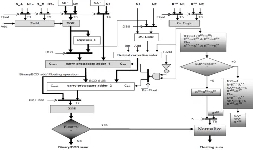
5. Hardware Efficient Reconfigurable 32-Bit Arithmetic Unit for Binary, BCD and Floating Point Operands The main goal of this chapter was to create an adder capable of carrying out binary, decimal and single precision floating point operations using effective addition/subtraction scheme. To achieve this we used both, arithmetic unit for reduced delay universal adder and arithmetic unit for 32-bit floating point adder as base. We combined the functionality of both arithmetic units to perform binary, decimal and floating point addition/subtraction operations on a single unit by combining the hardware of both arithmetic units as described in chapter-3 and chapter-4. The proposed adder depicted in Figure 5.1, Consider the operation SUM= N1 Add N2, with input signal Add indicates desirable addition/subtraction and SUM being the result of the operation. The addition/subtraction operation of two unsigned-magnitude numbers decided by Add input signal (Add=0 for addition & Add=1 for subtraction), while for signed-magnitude numbers addition/subtraction operation performed by the sign bits and Add input signal. Conclusion is that the addition/subtraction of two unsigned/signed- magnitude numbers can be performed with the determination of effective operation.
Assuming the operation involves true value of the signed numbers. The effective operation can be computed by the following Boolean expression:
Eadd indicates the effective operation in expression (5.1). If Eadd is equal to one, effective addition will be performed, and if Eadd is equal to zero, effective subtraction will be performed. The effective operations are described in Table 3.1.
Fig 5.1: Proposed Hardware Efficient Reconfigurable 32-Bit Arithmetic Unit
5.1 Single precision Floating point operations
In order to perform floating point operation, two input control signal Float and Bin are used to control and distinguish binary or BCD or floating point operation. The table 5.1 shows the control and operation.
Table 5.1: list of operations performed by input control signals
Float Bin Operation Performed
0 0 No operation
0 1 Binary floating point operations
1 0 Decimal operations
1 1 Binary operations
As shown in table if Float=0 and Bin=1 then binary floating point operation performed. Eadd logic, XOR (for input operand first complement), carry in circuitry including Co logic and all two colored blocks as shown in figure 5.1 are activated. The data flow from MUX units to logic blocks defined below:
T5=REA; T6=REB.
For carry in for carry-propagate-adder 1 and 2 controlled by a DEMUX and logic Bin.Float used as selected input for DEMUX. Another DEMUX used as a decision making logic and check whether control input Float is zero or not, if zero, floating point sum send to the normalize stage. Other XOR logic is used to complement the negative sum and its input T7 is the output of MUX which is controlled by logic Bin.Float. Other logic blocks are described in reduced delay universal adder.
5.2 Binary and BCD operations
In order to perform binary or BCD operation, input control signal Float kept at logic 1. Float=1 cause binary/BCD operation otherwise floating point operation is performed.
Therefore, for control signal Float=1, combined architecture works like reduced delay universal adder as already described.
When our proposed design mapped on partially reconfigurable hardware platform, the single colored dark modules (shown in figure 5.1: the Carry-propagate-adder 1, the Eadd logic, the two XOR logic blocks for one’s complement of input subtrahend and output SUM and the carry in logic circuitry including Co logic) are reused in both binary and BCD operation modes. The Eadd logic, both XOR logics, Carry in circuitry including Co logic and carry-propagate- adder 1 are reused in both binary/BCD and floating point operation modes.
6. Experimental results analysis and comparisons
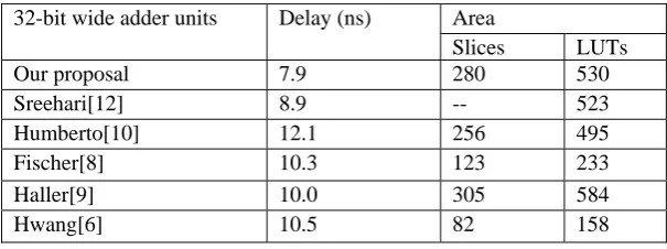
The proposed reduced delay adder was implemented using Verilog HDL, synthesized, functionally tested, and evaluated using the ISE 9.2i Xilinx design tools targeting 4vfx60ff672-12 VIRTEX 4 FPGA device. Furthermore, the designs proposed by Fischer [29], Hwang [27], Haller [19], Humberto[30] and sreehari[31] were also implemented and synthesized using same methodology. Table 6.1, summarizes the latency and hardware utilization result for all of the considered designs.
Table 6.1: Adder Comparison in terms of Area & Delay
In terms of latency the Sreehari proposal is best so far. Compared to it, our proposal is 11% faster with using almost equal hardware resources (LUTs) and in terms of area Hwang’s proposal is best design so far, but has the deficiency to produce correct result in cases when N1< N2 for BCD subtraction operations as described by humberto[10] . Also it uses only a single adder in its design.
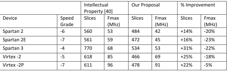
ISE simulator, simulation software was used to simulate allthe modules in a hierarchy design process. After the design was tested for functional correctness, the design was synthesized using Xilinx ISE 9.2i [41] synthesis tool provided by Xilinx which synthesize HDL for different Xilinx FPGAs intellectual property, proposed design was synthesized for all the devices the intellectual property is available for. Table 6.2 shows a comprehensive comparison between our results and theXilinx intellectual property.The Verilog HDL code was optimized for FPGA synthesis at modular level to insure best results both in-terms of area and latency. Pipelining exploits the unused flip-flops present in the slices of the recent FPGA architectures and thus have verysmall effect in area. The main improvement is achieved byplacing the pipeline stages at the proper places. Adder was synthesized separately for all the devices and the delay and area varied significantly was synthesized separately for all the devices andthe delay and area varied significantly explaining the variableclock speeds in different devices. In terms of area proposed design getting farbetter results than Xilinx Intellectual Property.
32-bit wide adder units Delay (ns) Area
Slices LUTs
Our proposal 7.9 280 530
Sreehari[12] 8.9 -- 523
Humberto[10] 12.1 256 495
Fischer[8] 10.3 123 233
Haller[9] 10.0 305 584
Table 6.2: Comparison of Xilinx Intellectual Property to the proposed design
The proposed Hardware Efficient Reconfigurable 32-Bit Arithmetic Unit for Binary, BCD and Floating Point Operands was implemented using Verilog HDL, synthesized, functionally tested, and evaluated using the ISE 9.2i Xilinx design tools targeting 4vfx60ff672-12 VIRTEX 4 FPGA device. Summarize in table 6.3.
Table 6.3: Hardware Efficient Reconfigurable 32-Bit Arithmetic Unit for Binary, BCD and Floating Point Operands logic unit design:
Hardware Resource Utilization Summary ⎯ targeting on 4VFX60FF672-12 device
SI. No. Device Parameter Number Usage Utilization %
1 Number of slices 653 2%
2 Number of slices Flip-Flop 319 0%
3 Number of 4-input LUTs 1224 2%
4 Number of IOs 231 -
5 Number of bounded IOBs 231 65%
6 Area Constraint Ratio 5 -
Table 6.3: Timing Summary ⎯ targeting on 4VFX60FF672-12 device
SI. No. Device Parameter Number Usage Utilization %
1 Number of slices 653 2%
2 Number of slices Flip-Flop 319 0%
3 Number of 4-input LUTs 1224 2%
4 Number of IOs 231 -
5 Number of bounded IOBs 231 65%
6 Area Constraint Ratio 5 -
The synthesis reports for the arithmetic unit for reduced delay universal adder as well as arithmetic unit for 32-bit floating-point adder on Virtex 4 family, 4VFX60 device, FF672 package with speed grade of -12 are shown in following manner :
Table 6.4, 6.5 and 6.6 are given here to show the resource utilization, Timing summery and comparison to the previous design respectively for the arithmetic unit for reduced delay universal adder.
Table 6.7 and 6.8 are given here to show the resource utilization & Timing summery respectively for the arithmetic unit for proposed floating point adder. Whereas Table 6.9 and 6.10 are given here to show the resource utilization and Timing summary respectively for Hardware Efficient Reconfigurable 32-Bit Arithmetic Unit for Binary, BCD and Floating Point Operands logic unit design.
Intellectual Property [40]
Our Proposal % Improvement
Device Speed Grade
Slices Fmax (Mhz)
Slices Fmax (MHz)
Table 6.4: Arithmetic Unit for Reduced Delay Universal Adder: Hardware Resource Utilization Summary ⎯ targeting on 4VFX60FF672-12 device
SI. No. Device Parameter Number Usage Utilization %
1 Number of slices 288 1%
2 Number of slices Flip-Flop 281 0%
3 Number of 4-input LUTs 530 1%
4 Number of IOs 131 --
5 Number of bounded IOBs 132 37%
6 Area Constraint Ratio 5 --
Table 6.5: Arithmetic Unit for Reduced Delay Universal Adder: Timing Summary ⎯ targeting on 4VFX60FF672-12 device
SI. No. Timing Parameter Proposed Adder Unit
1 Minimum Period 6.190 ns
2 Maximum Frequency 144.727 MHz
3 Minimum Input Arrival Time before Clock 7.981 ns 4 Maximum Output Required Time after Clock 3.793 ns
5 Gate Delay (Logic) 2.388 ns
6 Net Delay (Route) 5.593 ns
Table 6.6: Arithmetic Unit for Reduced Delay Universal Adder Comparison in terms of Area & Delay
“-“not specified by author
Table 6.7: Arithmetic Unit for 32-Bit Floating-Point Adder Logic Unit Design: Hardware Resource Utilization Summary – targeting on 4VFX60FF672-12 device
SI. No. Device Parameter Number Usage Utilization %
1 Number of slices 493 1%
2 Number of slices Flip-Flop 124 0%
3 Number of 4-input LUTs 925 1%
4 Number of IOs 100 --
5 Number of bounded IOBs 100 28%
6 Area Constraint Ratio 5 --
32-bit wide adder units Delay (ns) Area
Slices LUTs
Our proposal 7.9 288 530
Sreehari[12] 8.9 -- 523
Humberto[10] 12.1 256 495
Fischer[8] 10.3 123 233
Haller[9] 10.0 305 584
Table 6.8: Arithmetic Unit for 32-Bit Floating-Point Adder Logic Unit Design: Timing Summary –targeting on 4VFX60FF672-12 device
SI. No. Timing Parameter Proposed Adder Unit
1 Minimum Period 8.470ns
2 Maximum Frequency 118.064 MHz
3 Minimum Input Arrival Time before Clock 8.787 ns 4 Maximum Output Required Time after Clock 7.877 ns
5 Gate Delay (Logic) 2.593 ns
6 Net Delay (Route) 5.877 ns
Table 6.9: Hardware Efficient Reconfigurable 32-Bit Arithmetic Unit for Binary, BCD and Floating Point Operands Logic Unit Design. Hardware Resource Utilization Summary & comparisons – targeting on 4VFX60FF672-12 device
SI. No. Device Parameter Number Usage Utilization % Total Hardware resources used by
both design
% of sharing hardware resources
1 Number of slices 653 2% 781 16.4%
2 Number of slices Flip-Flop
319 0% 405 21.2%
3 Number of 4-input LUTs
1224 2% 1455 15.9%
4 Number of IOs 231 -- -- --
5 Number of
bounded IOBs
231 65% -- --
6 Area Constraint Ratio
5 -- 5 --
Table 6.10: Hardware Efficient Reconfigurable 32-Bit Arithmetic Unit for Binary, BCD and Floating Point Operands Logic Unit Design
Timing Summary – targeting on 4VFX60FF672-12 device
SI. No. Timing Parameter Proposed Adder Unit
1 Minimum Period 8.919ns
2 Maximum Frequency 112.120 MHz
3 Minimum Input Arrival Time before Clock 9.004 ns
4 Maximum Output Required Time after Clock 3.806 ns
5 Gate Delay (Logic) 3.175 ns
6 Net Delay (Route) 5.744 ns
7. Conclusion
sharing provided on Xilinx Virtex 4 FPGA chip. Place and Route static timing report suggests that maximum operating frequency for the Arithmetic unit for reduced delay universal adder is around 144 MHz and for the 32-bit floating point adder is around 118 MHz. However, Hardware Efficient Reconfigurable 32-Bit Arithmetic Unit for Binary, BCD and Floating Point Operands Logic Unit Design, it is around 112MHz. The operating speed of combined unit for binary, BCD and binary floating point adder is slower due to complexity increases of the design. The proposed combined arithmetic architecture has 8.9ns delay, 20% hardware resources are shared by both units together and achieve throughput of 112.3 MOPS using only 2% of the available hardware resources of the targeted FPGA.
References
[1] M.S.Schmookler and A. Weinderger. “Decimal Adder for Directly Implementing BCD Addition Utilizing Logic Circuitry”,
InternationalBusiness Machines Corporation,US patent 3629565, pages 1 – 19, Dec 1971.
[2] M. J. Adiletta and V. C. Lamere. “BCD Adder Circuit”. DigitalEquipment Corporation, US patent 4805131, pages 1 – 18, Jul 1989. [3] S. R. Levine, S. Singh, and A. Weinberger. Integrated Binary-BCD Look-Ahead Adder. International Business Machines
Corporation, US patent 4118786, pages 1–13, Oct 1978.
[4] J. L. Anderson. Binary or BCD Adder with Precorrected Result. Motorola, Inc., US patent 4172288, pages 1–8, Oct 1979. [5] U. Grupe.“Decimal Adder“, Vereinigte Flugtechnische Werke-Fokker gmbH, US patent 3935438, pages 1 – 11, Jan 1976.
[6] S. Hwang. “High-Speed Binary and Decimal Arithmetic Logic Unit”, American Telephone and Telegraph Company, AT&T Bell
Laboratories,US patent 4866656, pages 1-11, Sep 1989.
[7] Flora, Laurence P., “Fast BCD/Binary Adder”, US Patent 5007010.
[8] H. Fischer andW. Rohsaint. “Circuit Arrangement for Adding or Subtracting Operands Coded in BCD-Code or Binary-Code”,
SiemensAktiengesellschaft, US patent 5146423, pages 1 – 9, Sep 1992.
[9] W. Haller, W. H. Li, M. R. Kelly, and H. Wetter. “Highly Parallel Structure for Fast Cycle Binary and Decimal Adder Unit”.
InternationalBusiness Machines Corporation, US patent 2006/0031289, pages 1 – 8, Feb 2006.
[10] D.R.Humberto Calderón, G. N. Gaydadjiev, S. Vassiliadis, “Reconfigurable Universal Adder”, Proceedings of the IEEE International Conference on Application-Specific Systems, Architectures, and Processors (ASAP 07), pages 186-191, July 2007.
[11] Sreehari Veeramachaneni, M, Kirthi Krishna; V, Prateek G, S. Subroto, S, Bharat, M.B.Srinivas, “A Novel Carry-Look Ahead Approach to a Unified BCD and Binary Adder/Subtractor”, 21st International Conference on VLSI Design 2008, pages 547-552, Jan 2008.
[12] S. Vassiliadis, D. Lemon, and M. Putrino. s/370 Sign-Magnitude Floating-Point Adder. IEEE Journal of Solid-State Circuits, pages 1062 – 1070, Aug 1989.
[13] Govindu G., Zhuo L, Choi S., Prasanna V.: ‘Analysis of high performance floating-point arithmetic on FPGAS’. Proc. 18th Int. Symp. Parallel and Distributed Processing, 2004, pp. 149.
[14] Catanzaro B., Nelson B.: ‘Higher radix floating-point representations for FPGA-based arithmetic’. Proc. 13th Annual IEEE Symp.
Field-programmable Custom Computing Machines (FCCM’05), Washington, DC, USA, 2005, IEEE Computer Society, pp. 161– 170.
[15] Kavita Khare, R.P. singh and Nilay khare,”comparison of pipelined IEEE-754 standard floating point adder with unpipelined adder”.
![Figure 2. Fischer’s Proposal [8]](https://thumb-us.123doks.com/thumbv2/123dok_us/9653427.1493147/2.595.193.406.376.521/figure-fischer-s-proposal.webp)
![Figure 5. Sreehari’s Proposal [11]](https://thumb-us.123doks.com/thumbv2/123dok_us/9653427.1493147/4.595.235.453.94.244/figure-sreehari-s-proposal.webp)
![Figure 4.1: Algorithm of Pipelined Adder/Subtracter [37]](https://thumb-us.123doks.com/thumbv2/123dok_us/9653427.1493147/5.595.195.398.73.281/figure-algorithm-pipelined-adder-subtracter.webp)