University of Pennsylvania
ScholarlyCommons
Publicly Accessible Penn Dissertations
1-1-2014
Flexible Electronics Based on Solution Processable
Organic Semiconductors and Colloidal
Semiconductor Nanocrystals
Yuming Lai
University of Pennsylvania, [email protected]
Follow this and additional works at:
http://repository.upenn.edu/edissertations
Part of the
Electrical and Electronics Commons
,
Mechanics of Materials Commons
, and the
Nanoscience and Nanotechnology Commons
This paper is posted at ScholarlyCommons.http://repository.upenn.edu/edissertations/1337 For more information, please [email protected].
Recommended Citation
Lai, Yuming, "Flexible Electronics Based on Solution Processable Organic Semiconductors and Colloidal Semiconductor Nanocrystals" (2014).Publicly Accessible Penn Dissertations. 1337.
Flexible Electronics Based on Solution Processable Organic
Semiconductors and Colloidal Semiconductor Nanocrystals
Abstract
Solution-processable semiconductors hold great potential for the large-area, low-cost fabrication of flexible
electronics. Recent advances in flexible electronics have introduced new functional devices such as
light-weight displays and conformal sensors. However, key challenges remain to develop flexible devices from
emerging materials that use simple fabrication processes and have high-performance.
In this thesis, we first use a solution-processable organic semiconductor to build field-effect transistors on
large-area plastic with mobility of 0.1 cm^2/Vs. Combined with passive components, we are able to build
voltage amplifiers to capture few mV amplitude bio-signals. This work provides a proof of concept on applying
solution processable materials in flexible circuits.
In the second part of the thesis, we introduce colloidal CdSe nanocrystals (NCs) as solution-processable
"inks" of semiconductor thin film devices. By strongly coupling and doping the CdSe NC thin films, we
demonstrate high-performance, flexible nanocrystal field-effect transistors (NC-FETs) with mobility greater
than 20 cm^2/Vs under 2V supply. Using these NC-FETs as building blocks, we demonstrate the first flexible
nanocrystal integrated circuits (NCICs) with switching speed of 600 µsec. To design reliable integrated
circuits with low-noise, we characterize the flicker noise amplitude and origin. We find the figure of merit for
noise, the Hooge parameter, to be 3 x 10^-2 for CdSe NC-FETs, comparable to other emerging solution
processable organic semiconductors and promising for low-noise circuit applications.As most of NCs are
reactive and their devices tend to degrade in air, we develop processes that allow manipulation of the NCs in
ambient atmosphere without compromising device performance. These processes open up opportunities for
NC-based devices to be fabricated over large area using photolithography. By scaling the devices and reducing
device parasitics, we are able to fabricate hundreds of NC-FETs on wafer-scale substrates and integrate them
as circuits. We demonstrate voltage amplifiers with bandwidths of a few kHz and ring-oscillators with a stage
delay of 3 µsec. We also show functional NCICs NOR and NAND logic. This thesis demonstrates the use of
colloidal NCs to realize flexible, large-area circuits and the feasibility of more advanced analog and digital
NCICs built on flexible substrates for various applications.
Degree Type
Dissertation
Degree Name
Doctor of Philosophy (PhD)
Graduate Group
Electrical & Systems Engineering
First Advisor
Cherie R. Kagan
Keywords
Colloidal nanocrystals, Flexible electronics, Integrated circuits, Low frequency noise, Organic semiconductor,
Solution processable
Subject Categories
Electrical and Electronics | Mechanics of Materials | Nanoscience and Nanotechnology
FLEXIBLE ELECTRONICS BASED ON SOLUTION PROCESSABLE ORGANIC
SEMICONDUCTORS AND COLLOIDAL SEMICONDUCTOR NANOCRYSTALS
Yuming Lai
A DISSERTATION
in
Electrical and Systems Engineering
Presented to the Faculties of the University of Pennsylvania
in
Partial Fulfillment of the Requirements for the
Degree of Doctor of Philosophy
2014
Supervisor of Dissertation
________________________
Cherie R. Kagan
Stephen J. Angello Professor, Electrical and Systems Engineering
Graduate Group Chairperson
________________________
Saswati Sarkar
Professor, Electrical and Systems Engineering
Dissertation Committee
Jan Van der Spiegel, Professor, Electrical and Systems Engineering
Christopher B. Murray, Richard Perry University Professor, Chemistry
FLEXIBLE ELECTRONICS BASED ON SOLUTION PROCESSABLE ORGANIC
SEMICONDUCTORS AND COLLOIDAL SEMICONDUCTOR NANOCRYSTALS
COPYRIGHT
2014
Yuming Lai
This work is licensed under the Creative Commons Attribution- NonCommercial-ShareAlike 3.0 License
To view a copy of this license, visit
iv
ACKNOWLEDGMENT
First and foremost, I would like to thank Prof. Cherie Kagan for her guidance and financial
support in these years. I am deeply appreciated you give me countless advises through my study,
and always being very patient to teach and answer me, even for very fundamental questions.
Your broad knowledge in science and passionate attitude in research is always the model I am
pursing for.
I am very thankful my committee members and their input to my thesis and research.
Prof. Chris Murray provides guidance and invaluable knowledge in chemistry to my experiment.
Prof. Jan Van der Spiegel enthusiastically educates me on circuit theory and design, and help me
troubleshoot when they are not working as expected. I still remember a few late nights I work with
Prof. Jonathan Viventi, and see my designed circuits applied to animals as neural sensors. Those
experiments inspire me to think my research outside the box, and eventually turn into subjects in
my thesis.
I also want to thank my colleagues in Kagan group and Murray group. I enjoy working
with all of you, and thank you for your assist during these years. As both groups are growing so
big, please forgive me if I do not call out your name here. I would like to thank Dr. Sangam
Saudari. You are definitely my graduate mentor, and I am always grateful to do research and
learn from you in my first two years. I also thank my important collaborators, Dr. David Kim and
Benjamin Diroll. I am glad that we all have very similar working style that pushes out some
successful results. My circuit measurement won't be smooth without help from Shang Wei, Brian
Helfer, Scott Stinner and Hank Bink. I also want to thank Wenxiang Chen to work with me on
taking care our lab important tools. I am deeply appreciated E.D. Goodwin and Eric Wong for
those funny jokes and chats.
Besides colleagues in research group, I want to thank my friends, Albert Chen,
Chin-Chen Kuo and Chi-Mon Chin-Chen. As PhD students having kids, we can always share and complain
v
I am fortunate to have opportunities to use Quattrone Nanofabrication Facility, where they
provide various modern equipment important to my experiment. I want to say special thanks to
Kyle Keenan for his huge help on assisting me maintain our lab key equipments.
Last but not the least, I greatly thank my parents and my brother for their love and strong
support. Although we are always thousands miles apart for many years, you still send me your
warm encouragement whenever I need. I also want to thank my wife, Avon. I am so lucky to have
you, and I will never forget these busy years when we start our family with two lovely kids.
vi
ABSTRACT
FLEXIBLE ELECTRONICS BASED ON SOLUTION PROCESSABLE ORGANIC
SEMICONDUCTORS AND COLLOIDAL SEMICONDUCTOR NANOCRYSTALS
Yuming Lai
Cherie Kagan
Solution-processable semiconductors hold great potential for the large-area, low-cost
fabrication of flexible electronics. Recent advances in flexible electronics have introduced new
functional devices such as light-weight displays and conformal sensors. However, key challenges
remain to develop flexible devices from emerging materials that use simple fabrication processes
and have high-performance.
In this thesis, we first use a solution-processable organic semiconductor to build
field-effect transistors on large-area plastic with mobility of 0.1 cm2
/Vs. Combined with passive
components, we are able to build voltage amplifiers to capture few mV amplitude bio-signals. This
work provides a proof of concept on applying solution processable materials in flexible circuits.
In the second part of the thesis, we introduce colloidal CdSe nanocrystals (NCs) as
solution-processable "inks" of semiconductor thin film devices. By strongly coupling and doping
the CdSe NC thin films, we demonstrate high-performance, flexible nanocrystal field-effect
transistors (NC-FETs) with mobility greater than 20 cm2
/Vs under 2V supply. Using these
NC-FETs as building blocks, we demonstrate the first flexible nanocrystal integrated circuits (NCICs)
with switching speed of 600 µsec. To design reliable integrated circuits with low-noise, we
characterize the flicker noise amplitude and origin. We find the figure of merit for noise, the
Hooge parameter, to be 3 x 10⁻²
for CdSe NC-FETs, comparable to other emerging solution
vii
As most of NCs are reactive and their devices tend to degrade in air, we develop
processes that allow manipulation of the NCs in ambient atmosphere without compromising
device performance. These processes open up opportunities for NC-based devices to be
fabricated over large area using photolithography. By scaling the devices and reducing device
parasitics, we are able to fabricate hundreds of NC-FETs on wafer-scale substrates and integrate
them as circuits. We demonstrate voltage amplifiers with bandwidths of a few kHz and
ring-oscillators with a stage delay of 3 µsec. We also show functional NCICs NOR and NAND logic.
This thesis demonstrates the use of colloidal NCs to realize flexible, large-area circuits and the
feasibility of more advanced analog and digital NCICs built on flexible substrates for various
viii
TABLE OF CONTENTS
ACKNOWLEDGMENT ... iv
ABSTRACT ... vi
LIST OF TABLES ... xi
LIST OF ILLUSTRATIONS ... xii
CHAPTER 1 Introduction ... 1
1-1: Colloidal Semiconductor Nanocrystals ... 1
1-2: Outline of Thesis ... 2
1-3: References: ... 3
CHAPTER 2 Flexible Organic Electronics for Use in Neural Sensing ... 6
2-1: Bio-signal sensors ... 6
2-2: Flexible Pentacene Thin Film Transistors and Printed Circuit Board Design ... 8
2-3: Organic Electronics for Sensors with Amplification ... 10
2-4: Discussion and Conclusions ... 11
2-5: References ... 14
CHAPTER 3 High-Performance Nanocrystal Transistors and Integrated
Circuits on Flexible Plastic ... 16
3-1: Flexible and Low-Voltage Nanocrystal Field-Effect Transistor ... 16
3-2: Nanocrystal Integrated Inverters ... 19
3-3: Nanocrystal Integrated Voltage Amplifiers ... 21
3-4: Nanocrystal Integrated Ring Oscillators ... 22
3-5: Discussion ... 24
3-6: Conclusion ... 24
ix
3-8: Supplementary Information ... 27
3-9: References ... 37
CHAPTER 4 Low Frequency Noise in Nanocrystal Field-Effect Transistors ... 40
4-1: Models for flicker noise ... 40
4-2: Flicker Noise Relationship to Device Geometry ... 42
4-3: Device Hysteresis and Bias-Stress Effects ... 46
4-4: Flicker Noise in Nanocrystal Field-Effect Transistors ... 48
4-5: Nanocrystal Charge Transport and Flicker Noise Mechanism ... 50
4-6: Conclusion ... 53
4-7: Methods ... 53
4-8: Supplementary Information ... 55
4-9: References ... 62
CHAPTER 5 Recoverable Nanocrystal Field-Effect Transistors for Fabrication
and Operation in Air ... 66
5-1: Recovery of Degraded Nanocrystal Field-Effect Transistors ... 66
5-2: Air-Stable High Performance Devices on Wafer Scale Substrates ... 70
5-3: Conclusions ... 73
5-4: Methods ... 73
5-5: References ... 74
CHAPTER 6 Direct Photolithographic Patterning of Device Electrodes on
Colloidal Nanocrystals Thin Films to Build Wafer-Scale, Integrated Circuits .. 75
6-1: VIA Process and Transistors Characteristics ... 76
6-2: Inverters Characteristics and Analysis ... 80
6-3: NOR logic ... 83
6-4: NAND logic ... 83
x
6-6: Conclusion ... 86
6-7: Methods ... 86
6-8: Reference ... 87
CHAPTER 7 Future Direction ... 91
7-1: Photolithographic Patterning of Nanocrystal Thin Films to Build Integrated Circuitry on Flexible Plastic ... 91
7-2: Mechanical Stability of Flexible Nanocrystal Field-Effect Transistors ... 101
7-3: References ... 105
xi
LIST OF TABLES
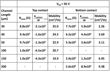
Table 4-1. Device resistances extracted using the transmission line method and carrier mobilities for TC and BC devices. All data shown is at VGS = 50 V. Note: Only saturation regime mobilities
are presented in this table, as mobility for NC-FETs is weakly dependent on VDS. 30
... 44
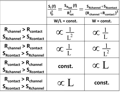
Table 4-2. Length dependent normalized drain current spectral density relationship for W/L= constant and W= constant. ... 45
xii
LIST OF ILLUSTRATIONS
Figure 2-1. (A) Schematic of the organic thin film transistor, a photographic example of which is seen in (B). (C) and (D) are the representative ID-VDS and ID-VGS properties of the devices,
respectively. The channel width is 1500 µm and length is 100 µm. These properties were measured in an inert nitrogen environment. ... 8
Figure 2-2. The dual PCB board design. The large board contains all elements of the circuit excluding the transistor: the amplifying resistor, low-pass power supply filters, output buffer and high-pass filter, and input/output components. The ribbon cable attaches the transistor to the rest of the circuit. The enlarged image on the left clearly shows the copper fingers used to make pressure contact with the organic TFT underneath. ... 9
Figure 2-3. Results from common source amplifier using pentacene TFT showing the (A) representative output versus input and (B) bode plot. Both results shown were taken from the same 100 µm channel length device. ... 11
Figure 2-4. Organic electronic sensor for recording neural signal. (Blue) Pre-recorded human EEG signal, and (Red) measured output from organic electronic sensor. The output signal was inverted for clear comparison. ... 12
Figure 3-1. Flexible CdSe nanocrystal field-effect transistors (NC-FETs). (A) Schematic and (B) photograph of a flexible CdSe NC-FET atop a Kapton® substrate. (C) Output ID – VDS and (D)
transfer ID – VG characteristics of a flexible, CdSe NC-FET. ... 18
Figure 3-2. Flexible nanocrystal integrated circuit (NCIC) inverter constructed from nanocrystal field-effect transistors (NC-FETs). (A) Photograph and (B) circuit schematic of saturated-load inverters. (1) Load NC-FET and (2) Driver NC-FET. (C) Graphical analysis of constituent driver (black) and load (red) NC-FET output characteristics, sweeping in forward and reverse, comprising the NCIC inverter, and (D) the corresponding voltage transfer characteristics (black, left axis) and gain characteristics (blue, right axis) of the NCIC inverter sweeping forward and reverse at a supply voltage of 2 V (VDD). ... 20
Figure 3-3. Flexible nanocrystal integrated circuit (NCIC) amplifier and Bode plot. (A) Output waveform (blue, right axis) of NCIC voltage amplifier in response to a 50 Hz, 100 mV sinusoidal input on a 0.6V DC bias (black, left axis). (B) Frequency response of a voltage amplifier (black circles). A linear fit (red solid line) shows a 4.59 dB voltage gain at low frequency which is used to find the 3 dB bandwidth (blue dashed line). ... 22
Figure 3-4. Flexible nanocrystal integrated circuit (NCIC) ring oscillator constructed from NCIC inverters. (A) Photograph, (B) circuit schematic and (C) output characteristics of a five-stage NCIC ring oscillator with a sixth stage buffer operating at a supply voltage of 2 V (VDD) with a
frequency of 165 Hz. ... 23
Figure 3-S1. Gate leakage current of 30 nm Al2O3 atomic layer deposited dielectric. The
xiii
Figure 3-S2. Back-gate/bottom-contact CdSe nanocrystal field-effect transistors (NC-FETs). (A) Schematic and (B) output (ID-VDS) and (C) transfer (ID-VG) curves...27
Figure 3-S3. Graphical and Noise Analysis of CdSe nanocrystal integrated circuit (NCIC) inverter. (A) Graphical analysis, only shown to magnifying low ID to 20 µA. (B) the constructed
points (red) versus measured (black) voltage transfer characteristic (VTC) for a CdSe NCIC inverter on a plastic substrate. (C) The original VTC (black solid line) overlaid with its mirror image (red solid line). VIN= VOUT(blue dashed line). The inscribed gray squares define the noise
margin high and noise margin low to be 0.1 V. Inverter Operation: The fabricated inverter is based on a saturated-load design [Figure 3-2 (A, B)], where one n-type field-effect transistor (FET) acts as an active load and the other n-type FET as a driver. The load FET has its source connected to the inverter’s output (VOUT) and its drain and gate are both connected to the
inverter’s supply voltage (VDD). The load FET always operates in saturation because the gate
and drain-source voltages are identical ensuring that −< for a positive
threshold voltage. The driver FET has its gate connected to the inverter’s input (VIN), its drain
connected to the inverter’s output (VOUT) and its source connected to ground (VSS). During device
operation when the inverter input is “low” (VIN = 0), the driver FET is in the off-state and exhibits
very large resistance. The supply voltage will be divided dropping across the more resistive driver FET than load FET, causing the output voltage to exhibit a “high” voltage that is about the difference between the supply voltage and the load’s threshold voltage () =− . When the input of the inverter is “high” =, the driver FET will be in the on-state and
exhibit very low resistance. The divided voltage will now be predominantly across the load, causing the output node to exhibit a “low” voltage that is close to ground. Inverter Voltage Transfer Characteristics: Graphical analysis of the load and driver FET intercept points are used to construct the inverters’ VTCs.30
The low hysteresis in the NCIC VTCs provides adequate noise margin at both logic high and low regions. Noise margin is evaluated by taking the original VTC overlaid with its’ mirror image (VIN = VOUT as mirror plane). The largest inscribed square area
defines the inverter’s noise margin.41 The noise margin ensures the inverter functions correctly in
complex integrated circuits, providing logic switching (eg. in the 1st
inverter stage, 0.4 V input will output at 1.3 V, and this 1.3 V is the input for the 2nd
stage inverter and output at 0.4 V.) ... 29
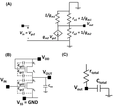
Figure 3-S4. CdSe Nanocrystal Integrated Circuit (NCIC) Amplifier Equivalent Circuit Modeling. (A) Small-signal equivalent-circuit model of a common-source amplifier with a saturated-load design. (B) Schematic of parasitic and interconnect capacitances. (C) The simplified model from Supplementary Figure 3-S4 (A) and Figure 3-S4 (B)...30
Figure 3-S5. Propagation delay definitions in the inverter’s output waveform. ... 31
Figure 3-S6. CdSe Nanocrystal Integrated Circuit (NCIC) Ring Oscillator Equivalent Circuit Modeling. An example of parasitic capacitance for a 3-stage ring oscillator with an additional inverter serving as a buffer. Note that the Miller effect is applied to Cgd2. ... 31
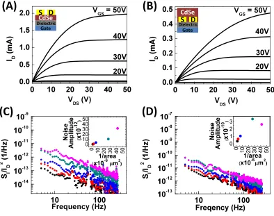
Figure 4-1. Device output characteristics (ID-VDS) for (A) top-contact and (B) bottom-contact
CdSe NC-FETs. Normalized drain current spectral density (SI/ID
2) vs frequency for (C) top-contact
xiv
Figure 4-2. Normalized drain current spectral density (SI/ID 2
) as a function of channel length varying from 30 µm to 200 µm, collected at a fixed frequency of 10 Hz, VDS = 50 V and VGS = 50
V. (A) Representative channel length dependence of SI/ID
2 for top-contact (red) and
bottom-contact (green) devices with a constant W/L of 15. (B) Channel length dependence of SI/ID 2
for top-contact devices with constant W/L (blue) and fixed channel width of 1800 µm (cyan). Note: The device channel length of 90 µm and channel width of 1800 µm is common, representing the constant W/L ratio of 20 and the constant channel width of 1800 µm. Slopes of m = -1 and m = -2 lines are shown for reference. ... 46
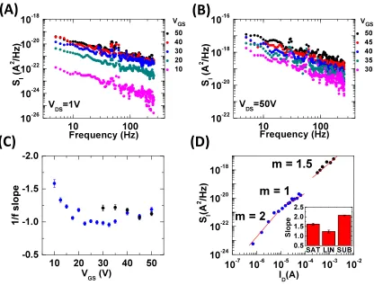
Figure 4-3. Spectral current density (SI) of Al2O3-encapsulated, top-contact devices as a function
of frequency measured at (A) VDS = 1 V and (B) VDS = 50 V under various VGS. (C) 1/f slope fit
from SI vs frequency as a function of VGS at VDS = 1 V (blue) and VDS = 50 V (black). (D) SI vs ID
at a frequency of 10 Hz for devices biased in saturation at VDS = 50 V (black) and linear and
subthreshold regimes at VDS = 1 V (blue). Slopes (m) of 1, 1.5 and 2 are drawn for reference.
Inset: Statistics from 4 devices of the slope of SI vs ID, measured in the saturation, linear and
subthreshold regimes respectively. ... 48
Figure 4-4. Mobility and Hooge parameter (αH) as a function of VGS when VDS = 50 V for (A)
unencapsulated, top-contact and (B) Al2O3-encapsulated, top-contact devices. Insets in (A) and
(B) are NC-FET schematics. (C) Schematic of the carrier concentration in the NC-FET channel, and (D) the density of states for NC thin films and the energy of the Fermi level in the linear (red), saturation (green), and subthreshold (orange) regimes. E0 denotes the mobility edge. Note, in the
saturation region pinch off within ∆L of the drain electrode causes the Fermi energy to move further away from the band edge. The density of tail states (blue dashed) is reduced after Al2O3
encapsulation (blue solid). ... 51
Figure 4-S1. (A) Representative transfer characteristics (ID-VGS) for top-contact (red) and
bottom-contact (black) devices, with L = 50 µm and measured at VDS = 50 V. The contact (Rcontact) and
channel (Rchannel) resistances are extracted from the total resistance (Rtotal) as a function of
channel length using the transmission line method for (B) top-contact and (C) bottom-contact devices respectively, collected at VGS = 30 V (black), VGS = 40 V (red), and VGS = 50 V (blue). (D)
A representative SI/ID 2
vs frequency of a top-contact, L = 40 µm device measured in the saturation and linear regimes, showing that noise is weakly dependent on VDS. ... 57
Figure 4-S2. Statistics of the length dependence of SI/ID 2
for different scaling of the device geometry. ... 58
Figure 4-S3. Time dependence of the normalized drain-source current (ID) measured under a
voltage stress of (A) VDS = 50 V and (B) VDS = 1 V for an unencapsulated, top-contact device
(dashed lines) and an Al2O3-encapsulated, top-contact device (solid lines), where VGS = 50 V
(black), VGS = 40 V (red), VGS = 30 V (blue) and VGS = 20 V (green). ... 59
Figure 4-S4. Device transfer characteristics ID-VGS for (A) an unencapsulated, top-contact and
(B) an Al2O3-encapsulated, top-contact device at VDS = 50 V and VDS = 1 V (inset), where ID-VGS
before (black) and after (red) noise collection are presented. The average stress current during noise collection is shown as blue stars at each applied bias and is the average of the current collected in Fig. 4-S3 from 10 sec to the end of applied bias at 70 sec. Note: the calculated interface trap density from the subthreshold swing is 9.67 x 10¹²
cm-2
for (A) and 9.14 x 10¹²
cm-2
xv
Figure 4-S5. Traces of ID as a function of time under voltage stress (black) and fits to a stretched
exponential function (red) for (A) an unencapsulated, top-contact and (B) an Al2O3-encapsulated,
top-contact device under VDS = 1 V, VGS = 50 V and for (C) an unencapsulated, top-contact
device and (D) an Al2O3-encapsulated, top-contact device under VDS = 50 V, VGS = 50 V. Insets in
(A-D) show fitting parameters (τ and β) as a function of VGS. ... 60
Figure 4-S6. (A) Representative SI/ID 2
vs (VGS-VT) characteristics at a frequency of 10 Hz for an
Al2O3-encapsulated device operated in the linear regime (VDS = 1 V). The slope fit for frequencies
between 5 to 10 Hz in a step of 1 Hz is -0.9 ± 0.15. Slopes of -1 and -2 are drawn for reference. (B) Representative SI vs (VGS-VT) at a frequency of 10 Hz for an Al2O3-encapsulated device
operated in the saturation regime (VDS = 50 V). The slope fit for frequencies between 5 to 10 Hz
in a step of 1 Hz is 3.1 ± 0.27. Slopes of 2 and 3 are drawn for reference. (C) Comparison of the SI/ID
2
and SI dependence on (VGS -VT) for the Hooge (∆µ) and McWhorter (∆N) models for devices
operated in linear and saturation modes... 61
Figure 4-S7. Mobility and Hooge parameter (αH) as a function of VGS when VDS = 1 V for (A)
unencapsulated, top-contact and (B) Al2O3-encapsulated, top-contact devices. ... 62
Figure 5-1. CdSe NC-FET on-current (VG=50 V) in the linear regime (VDS=5 V) monitoring (A)
cyclic degradation as a function of air exposure time and recovery upon re-annealing at 200 o
C for 5 min, (B) degradation in air versus in pure oxygen environments (open bar : initial, filled bar : exposure), and (C) the evolution in as-prepared FETs (black) upon successive cycles of air exposure for 30 min (red) and recovery by annealing at 200 o
C for 5 min (blue). (D) Statistics in on-current recovery after 5 min of annealing at different temperatures. Note: Since all devices recover at an annealing temperature of 200 o
C, the scale is narrowed. (E) NC-FET degradation, characterized by the decrease in drain current IDS (after exposure) to IDSO (initial), upon immersion
in acetone, chloroform, isopropanol, methanol and water for 10 min at room temperature. Samples were dried using a nitrogen stream before electrical measurement. (Top) On-current recovery upon re-annealing at 200 o
C for 5 min after solvent immersion. ... 67
Figure 5-2. ID-VG characteristics of CdSe NC-FETs before and after repeated cycling through 13
times of air exposure and annealing. ... 69
Figure 5-3. (A) A photograph of an array of 144 transistors fabricated by photolithographically patterning source and drain electrodes on [inset] a uniformly spin-cast CdSe NC thin film across a 4 inch Al2O3(20 nm)/SiO2(250 nm)/highly-doped Si wafer. (b) Output and (c) transfer
characteristics (VDS=5 V) of NC-FETs (channel length L=30 µm, width W=450 µm). [inset (b)]
Schematic of the device structure. (d) Electron mobility of integrated CdSe NC devices over the large-area 4 inch substrate. (e) NC-FET electron mobility (black) and threshold voltage (blue) as a function of time stored and operated in air. ... 71
Figure 5-4. (A) A photograph of an array of photolithographically patterned NC-FETs on a 4 inch square Kapton® substrate. (b) Output and (c) transfer characteristics (VDS =0.1 and 2 V) of
NC-FETs (channel length L=30 µm, width W=450 µm). [inset] Schematic of the NC-FET structure. .. 72
Figure 6-1. (A) Photograph of wafer-scale CdSe NCICs, where the smallest channel length is 5 µm. (B) Schematic of (top) single transistor and (bottom) transistor with VIA connection to form enhancement-load inverters. (C) Device output characteristics (ID-VDS) and (D) transfer
characteristics (ID-VGS) in the saturation regime (VDS = 3 V). Channel width over channel length is
xvi
Figure 6-2. (A) The unit capacitance and dielectric constant (epsilon) of ALD grown Al2O3 as a
function of frequency. The average epsilon measured from 8 test capacitors is 7.3 ± 0.48 (at 2 kHz). (B) Device transfer characteristics operated in the linear regime (VDS = 0.1 V). Channel
width over length is (600 µm/40 µm). (C) Transmission line method used to characterize device contact resistance for devices with channel lengths ranging from 5 µm to 40 µm, under (Black) VGS = 1.5V, (Red) VGS = 2.0V and (Blue) VGS = 2.5V. (D) A summary of extracted contact and
channel resistance from the transmission line method. ... 78
Figure 6-3. Nanocrystal integrated inverter and electrical characteristics. (A) Photograph of an enhancement-load inverter, where (W/L)Load to (W/L)Driver ratio is (10/100), and the channel
lengths are constant at 10 µm. (B) Inverter voltage transfer characteristics at (black) VDD = 5 V,
(red) 4 V, (blue) 3 V and (olive) 2 V and its associated (C) voltage gain, (D) noise margin and (E) drain current. Voltage amplifier output characteristics for input at (F) 10 Hz and (G) 5 kHz, where (red) output waveform is in response to (black) input signal. (H) Bode plot of voltage amplifier, where blue dashed lines refer to low frequency voltage gain and 3 dB gain at higher frequency. ...79
Figure 6-4. (A) Top and perspective view of VIA test structures, where the red layer is the gate electrode, yellow is the VIA, and blue is the source/drain electrodes. The square VIAs have sizes of 200, 100, 50 and 25 µm. (B) I-V characteristics across 16 VIA holes, described as yellow arrows in (A). ... 81
Figure 6-5. Nanocrystal integrated NOR and NAND logics. Photograph of (A) NOR and (D) NAND, where the load FET has a fixed (W/L) ratio of 10 and the driver FETs have a fixed (W/L) ratio of 100. Channel length is constant at 10 µm for load and driver FETs. Circuit symbol and truth table for (B) NOR and (E) NAND logic gates. Voltage transfer characteristics for (C) NOR and (F) NAND logics, where black and blue scans refer to different input configurations, shown as black and blue arrows in (B),(E) truth tables. ... 82
Figure 6-6. Nanocrystal integrated 5-stage ring oscillators. (A) Photograph and circuit schematic. (B) Output waveform of a 5-stage ring oscillator at VDD = 5 V. (C) Stage delay statistics as a
function of VDD. (D) Summary of the ring oscillator stage delay using active channels from the
following classes of solution processable.materials:(green) organic semiconductor, (blue) carbon nanotube networks, (red) metal-oxides, and (black) for colloidal nanocrystal semiconductors (demonstrated in this thesis). Solid circles represent reports of devices fabricated on rigid substrates, and empty circles for devices on flexible plastics. The black empty diamond is the 1st NCIC ring oscillator fabricated on flexible substrate, reported in Chapter 3. ... 85
Figure 7-1. (A) Photograph of a large-area, photolithographically-patterned, CdSe nanocrystal thin film. (B) Optical micrograph of a patterned nanocrystal thin film array, where the gap and pitch are both 25 µm. ... 92
Figure 7-2. (A) Photograph of 10 x 10 cm square flexible nanocrystal integrated circuit, where CdSe nanocrystals are patterned. (B) Schematic of devices with and without patterned nanocrystals. (C) Optical micrograph of devices with patterned nanocrystals as the active channel (top), and an array of the patterned nanocrystal thin film (bottom). (D) At constant VDS = 5 V,
device drain current (ID, black, left y-axis) and gate current (IG, blue,right y-axis) for non-patterned
(empty circle) and patterned (solid) nanocrystal thin-film devices. Device channel width over length ratio is 1000 µm / 10 µm. (E) ALD grown Al2O3 gate leakage current as a function of
xvii
Figure 7-3. Schematic of a nanocrystal thin-film transistor (A) without and (C) with ALD Al2O3
encapsulation. Transfer characteristics (ID-VGS, black, left axis) and its square root (blue, right
y-axis) in the saturation regime (VDS = 5 V) for devices (B) without and (D) with 50 nm ALD Al2O3
encapsulation. (E) Output characteristics (ID-VDS) and (F) statistics on carrier mobility (µ),
threshold voltage (VT), subthreshold swing (S) and dielectric-semiconductor interface trap density
(NT) for encapsulated devices. Note: Device channel width over length ratio is 1000 µm / 10 µm in
(B,D,E). Saturation regime characteristics are measured at VDS = 5 V, and linear regime
characteristics are measured at VDS = 0.1 V. ... 94
Figure 7-4. (A) Transmission line method for devices with constant channel width to length ratio of 15, and channel length ranging from 5 µm to 40 µm. (B) Extracted device channel resistance (RCH) and metal-to-semiconductor contact resistance (RCONTACT) as a function of gate voltages. 95
Figure 7-5. Enhancement-load inverter. Voltage transfer characteristics for device (A) without and (C) with encapsulation. Noise margin for devices (B) without and (D) with encapsulation. The channel width (W) to length (L) ratio is 10 for the load, and 100 for driver. Load and driver transistors have constant channel length of 10 µm. ... 96
Figure 7-6. (A) Photograph of enhancement-load inverter. (B) Load (red) and driver (black) output characteristics. (C) Inverter voltage transfer characteristics, (D) voltage gain, (E) noise margin, and (F) drain current for (black) VDD = 5 V, (red) 4 V, (blue) 3 V and (olive) 2 V. Voltage
amplifier characteristics for an input at (G) 10 Hz and (H) 16 kHz, where (red) the output waveform is measured in response to (black) a sinusoidal, 200 mV peak-to-peak input signal. (I) Bode plot for the voltage amplifier, where blue dashed lines refer to low frequency voltage gain and 3 dB gain at higher frequency. The measured 3dB bandwidth is ~ 16 kHz. ... 100
Figure 7-7. Inverter dynamic response at VDD = 5 V. Input (black) and output (red) waveform for
(A) 100 Hz 5 V peak to peak input, and (B) 10 kHz 5 V peak to peak input. ... 100
Figure 7-8. (A) Photograph of NOR logic. (B) Voltage transfer characteristics for different input sweep configurations, where black refers to the input sweep between [0,0] and [1,1], and blue refers to the input sweep between [0,0] and [0,1]. Inset: NOR truth table. (C) Output characteristics. ... 100
Figure 7-9. Schematic for a beam under bending.3
... 101
Figure 7-10. Photograph of (A) tension and (B) compression measurement setup. ... 102
Figure 7-11. (A) Top: Schematic of device under tension and compression tests. Bottom: Device mobility (black) and threshold voltage (VT, blue) relationship to strain in the saturation (VDS = 2 V)
and linear (VDS = 0.1 V) regimes. (B) Photograph of device wrapped around a radius of ~ 1.0 mm
to emulate extreme bending, equal to -2.5% strain. (C) Device transfer characteristics (ID-VG) in
saturation (VDS = 2 V) and linear (VDS = 0.1 V) regime under flat (black), -2.5 % strain (blue) and
returned to flat after bending (red). ... 103
Figure 7-12. Device output characteristics (ID-VDS) when sample is (A) flat, (B) under -2.5 %
strain, and (C) returned to flat. Gate leakage current (IG-VDS) when sample is (D) flat, (E) under
xviii
Figure 7-13. Change in oxide capacitance versus strain, normalized to the original flat oxide capacitance. ... 105
1
CHAPTER 1 Introduction
1-1: Colloidal Semiconductor Nanocrystals
Colloidal semiconductor nanocrystals (NCs) are prized for their size- and shape-tunable
electronic properties.1–4
Wet-chemical methods have enabled the preparation of highly uniform,
monodisperse, crystalline NCs for a wide variety of chemical compositions by commonly
employing long-chain, organic ligands to control NC synthesis and to stabilize NC dispersions.5
These NC solutions capped with long ligands can be easily processed by a variety of
solution-based material deposition methods (spincasting, dipcoating, inkjet printing, dropcasting,
spraycoating) to form uniform thin-films.6–11
While high quality NC synthesis and dispersibility
relies on long ligands, these ligands are insulating and prevent strong coupling and charge
transport between NCs once assembled in the solid state. Until recently, this has posed a
significant challenge to using these colloidal inks as technologically viable electronic materials for
devices12
and integrated circuitry.13
Advances in ligand chemistry have shown that the original,
long ligands used in synthesis can be replaced by shorter inorganic ligands14–17
either in solution,
and still maintain solution-dispersibility and thin-film processability, or in thin-film solids. These
novel ligands preserve the discrete, size-dependent features of quantum confinement and
enhance electronic coupling between the NCs in thin-films. Our group, along with the Talapin
group, have shown that dispersions of NCs exchanged with compact ligands can be spincast to
form dense, crack-free, thin-films that demonstrate excellent performance in single field-effect
transistors (FETs), with high electron mobilities exceeding 15 cm2
V-1
s-1
.16,18–20
The
solution-processability and high-performance of NC-FETs make colloidal NC semiconductors extremely
attractive as colloidal inks for low-cost, large-scale coating and printing of thin-film electronics.
While there has been significant progress in developing single high mobility NC-FETs that further
operate with low-hysteresis18,20
at low-voltage,21
these high-performance NC-FETs have not been
2
single separate FETs connected externally to form an inverter.21,22
In order to realize nanocrystal
integrated circuits (NCICs) for large-area, thin-film electronics, it is necessary to go beyond
discrete FET fabrication, to integrate multiple FETs into circuits and to evaluate device operation,
such as the switching speed and signal amplification of the NC-FET. This requires that NC
thin-films be processed and deposited over a large area to form uniform devices that operate in
concert as circuits.
1-2: Outline of Thesis
The goal of this thesis is to use solution processable materials in flexible electronics and
demonstrate high density, large-area, low-voltage integrated circuits on flexible plastic. In
Chapter 2, we first use solution processable precursor to pentacene the organic semiconductors
to fabricate large-area, flexible FETs with hole mobility of 0.1 cm2
/Vs. We integrate them with
passive resistors on printed circuit board to realize voltage amplifiers. We demonstrate these
amplifiers is able to capture mV bio-signals. In Chapter 3, we use colloidal CdSe NCs as active
materials. The original long insulating organic ligands is replaced with compact thiocyanate to
greatly enhance coupling between NCs. The non-corrosive thiocyanate allows fabrication
compatible to flexible plastics. These NC thin films is then doped by thermal diffusion of indium
metals introduced at device electrodes. With strong coupling and doping of NCs, we construct
high-performance NC-FETs with electron mobility greater than 20 cm2
/Vs. Using NC-FETs as
building blocks, we fabricate nanocrystal integrated circuits (NCICs) including voltage amplifier,
inverters and ring oscillators. The highest switching speed is 600 µs with supply voltage of 2V. In
Chapter 4, in order to evaluate the noise level for designing reliable circuits with low noise, we
investigate the low-frequency noises in CdSe NC-FETs. We characterize the noise level and
origin. By engineering device geometries and passivating NC surface traps, we find flicker noise
in NC-FETs relates to charge transport through NC electronic structures. We report a figure of
merit for noise, Hooge parameter in CdSe NC-FETs to be 3 x 10⁻²
, comparable to other solution
3
most of NCs are reactive and their electronic properties degrade in exposure to air or chemical
solvents, NC fabrication are generally limited to inert atmosphere. In Chapter 5, we introduce NCs
recovery mechanism where their electronic properties can be repaired, through indium metals to
passivate trap states formed during exposure to air and chemicals. The recovery effects allow NC
to be processed with various techniques in ambient environment, such as large-area
photolithographic patterning or device encapsulation by atomic layer deposition. The
encapsulated NC-FETs show stable operation in air for more than 2 months. In Chapter 6, we
use photolithography to scale high performance NC-FETs to fabricate hundreds of devices, and
integrate them as circuits on four inch Si wafer. The reduced parasitic capacitance pushes the
switching speed to 3 µs. In Chapter 7, we take advantage of wet etcher to selectively remove
CdSe NC thin films to form defined active channels. We successfully translate this to flexible
plastic and demonstrate large-area, flexible NCICs with patterned active layers.
1-3: References:
(1) Bawendi, M. G.; Steigerwald, M. L.; Brus, L. E. The Quantum Mechanics of Larger Semiconductor Clusters (“Quantum Dots”). Annu. Rev. Phys. Chem. 1990, 41, 477–496.
(2) Alivisatos, A. P. Semiconductor Clusters, Nanocrystals, and Quantum Dots. Science (80-. ). 1996, 271, 933–937.
(3) Murray, C. B.; Kagan, C. R.; Bawendi, M. G. Synthesis and Characterization of Monodisperse Nanocrystals and Close-Packed Nanocrystal Assemblies. Annu. Rev. Mater. Sci. 2000, 30, 545–610.
(4) Efros, A. L.; Rosen, M. The Electronic Structure of Semiconductor Nanocrystals. Annu. Rev. Mater. Sci. 2000, 30, 475–521.
(5) Murray, C. B.; Norris, D. J.; Bawendi, M. G. Synthesis and Characterization of Nearly Monodisperse CdE (E= S, Se, Te) Semiconductor Nanocrystallites. J. Am. Chem. Soc.
1993, 115, 8706–8715.
(6) Mitzi, D. B.; Kosbar, L. L.; Murray, C. E.; Copel, M.; Afzali, A. High-Mobility Ultrathin Semiconducting Films Prepared by Spin Coating. Nature 2004, 428, 299–303.
4
(8) Wood, V.; Panzer, M. J.; Chen, J.; Bradley, M. S.; Halpert, J. E.; Bawendi, M. G.; Bulović,
V. Inkjet-Printed Quantum Dot-Polymer Composites for Full-Color AC-Driven Displays. Adv. Mater. 2009, 21, 2151–2155.
(9) Talapin, D. V; Murray, C. B. PbSe Nanocrystal Solids for N- and P-Channel Thin Film Field-Effect Transistors. Science (80-. ). 2005, 310, 86–89.
(10) Soreni-Harari, M.; Mocatta, D.; Zimin, M.; Gannot, Y.; Banin, U.; Tessler, N. Interface Modifications of InAs Quantum-Dots Solids and Their Effects on FET Performance. Adv. Funct. Mater. 2010, 20, 1005–1010.
(11) Kovalenko, M. V; Spokoyny, B.; Lee, J.-S.; Scheele, M.; Weber, A.; Perera, S.; Landry, D.; Talapin, D. V. Semiconductor Nanocrystals Functionalized with Antimony Telluride Zintl Ions for Nanostructured Thermoelectrics. J. Am. Chem. Soc. 2010, 132, 6686–6695.
(12) Talapin, D. V; Lee, J.-S.; Kovalenko, M. V; Shevchenko, E. V. Prospects of Colloidal Nanocrystals for Electronic and Optoelectronic Applications. Chem. Rev. 2010, 110, 389– 458.
(13) Yun, J.; Cho, K.; Kim, S. Flexible Logic Circuits Composed of Chalcogenide-Nanocrystal-Based Thin Film Transistors. Nanotechnology 2010, 21, 235204.
(14) Kovalenko, M. V; Scheele, M.; Talapin, D. V. Colloidal Nanocrystals with Molecular Metal Chalcogenide Surface Ligands. Science 2009, 324, 1417–1420.
(15) Nag, A.; Kovalenko, M. V; Lee, J.-S.; Liu, W.; Spokoyny, B.; Talapin, D. V. Metal-Free Inorganic Ligands for Colloidal Nanocrystals: S(2-), HS(-), Se(2-), HSe(-), Te(2-), HTe(-), TeS(3)(2-), OH(-), and NH(2)(-) as Surface Ligands. J. Am. Chem. Soc. 2011, 133, 10612–10620.
(16) Fafarman, A. T.; Koh, W.; Diroll, B. T.; Kim, D. K.; Ko, D.-K.; Oh, S. J.; Ye, X.; Doan-Nguyen, V.; Crump, M. R.; Reifsnyder, D. C.; et al. Thiocyanate Capped Nanocrystal Colloids: A Vibrational Reporter of Surface Chemistry and a Solution-Based Route to Enhanced Coupling in Nanocrystal Solids. J. Am. Chem. Soc. 2011, 133, 15753–15761.
(17) Rosen, E. L.; Buonsanti, R.; Llordes, A.; Sawvel, A. M.; Milliron, D. J.; Helms, B. a. Exceptionally Mild Reactive Stripping of Native Ligands from Nanocrystal Surfaces by Using Meerwein’s Salt. Angew. Chem. Int. Ed. 2012, 51, 684–689.
(18) Lee, J.-S.; Kovalenko, M. V; Huang, J.; Chung, D. S.; Talapin, D. V. Band-like Transport, High Electron Mobility and High Photoconductivity in All-Inorganic Nanocrystal Arrays. Nat. Nanotechnol. 2011, 6, 348–352.
(19) Chung, D. S.; Lee, J.-S.; Huang, J.; Nag, A.; Ithurria, S.; Talapin, D. V. Low Voltage, Hysteresis Free, and High Mobility Transistors from All-Inorganic Colloidal Nanocrystals. Nano Lett. 2012, 12, 1813–1820.
5
(21) Chung, D. S.; Lee, J.-S.; Huang, J.; Nag, A.; Ithurria, S.; Talapin, D. V. Low Voltage, Hysteresis Free, and High Mobility Transistors from All-Inorganic Colloidal Nanocrystals. Nano Lett. 2012, 12, 1813–1820.
Much of this chapter appears in print: © 2011 IEEE. Reprinted, with permission, from Bink, H.*; Lai, Y.*; Saudari, S.R.; Helfer, B.; Viventi, J.; Van der Spiegel, J.; Litt, B.; Kagan, C., "Flexible organic electronics for use in neural sensing," Engineering in Medicine and Biology
Society,EMBC, 2011 Annual International Conference of the IEEE pp.5400,5403, Aug. 30 2011-Sept. 3 2011
* Both authors contributed equally
6
CHAPTER 2 Flexible Organic Electronics for Use in Neural Sensing
2-1: Bio-signal sensors
Electrocorticography (ECoG), the process of recording brain activity through electrodes
placed directly on the cortical surface, is a common technique in the assessment and treatment of
neurological disorders, such as epilepsy. ECoG offers a higher spatial and temporal resolution
interface with the brain than extracranial electroencephalography (EEG), since the electrodes are
smaller and located at a much closer distance to the brain. Penetrating microelectrodes, such as
the Utah array,1
can measure neural activity at a higher spatial resolution, including from single
neurons, but are constrained to interface with small regions of the cortex. Further, the long-term
feasibility of this interface is often limited to only 6-12 months,2
either due tissue damage caused
by the inability of the rigid penetrating electrodes to flex and move as the brain swells and
contracts3
or by damage caused from hemorrhage and inflammation from the initial insertion4
.
ECoG does not appear to suffer from this stability issue and has demonstrated consistent signal
quality over extended periods of time with minimized irritation and injury to brain tissue.5,6
Further, ECoG and higher resolution micro-ECoG (µECoG) recordings from flexible
arrays of non-penetrating electrodes may offer comparable information content to the neural
signals recorded from penetrating electrodes in some applications, such as BMI,7–9
decoding
motor control signals10
and decoding spoken words.11
High resolution neural interface is also
important to understanding pathologic brain signals.12
In addition to high spatial resolution,
developing electrode arrays with a high degree of conformality is also important. Highly flexible
7
surface of the brain, resulting in higher signal to noise ratios in recordings and more electrodes in
contact with the brain.13 Current clinical ECoG arrays use metal electrodes that typically have a
diameter of 3 mm on a grid with 1cm center-to-center spacing.14
Because of these dimensions,
the arrays spatially undersample the electrical signals of the brain. µECoG electrode arrays have
been developed that utilize flexible silicon electronics to create a conformal, dense (800 µm
spacing) electrode array capable of covering large areas (14.4 mm x 12.8 mm) of the brain.15
These devices offer recordings with high spatial and temporal resolution and utilize on-chip
multiplexing to reduce the number of wires coming off the grid. Constructing these silicon devices
can be a difficult and expensive process. Alternatively, organic electronics may be able to be
fabricated at lower cost than flexible silicon electronics on the same type of plastic substrates.
Organic materials are considered a promising candidate for flexible electronics due to the
low temperatures required for fabrication. Through intensive research in the past decades,
organic materials have been shown to exhibit carrier mobility comparable to or higher than
amorphous silicon used in modern active-matrix liquid-crystal displays.16 In addition, synthetic
chemistry is able to tailor organic materials in a way that cannot be done with inorganics. The
increased functionality of organic transistors can enable a broad array of biological signal
monitoring applications. Pentacene, among the highest performance organic thin film
semiconductor materials available, is insoluble in most organic solvents. A soluble pentacene
precursor, developed by A. Afzali et al.,17
can be dissolved in a chlorinated solvent, such as
chloroform, and subsequently thermally converted into pentacene. This production technique
opens the door to large area fabrication of organic transistor circuits at low cost.
In this chapter, we demonstrate solution processable organic thin film transistors that can
be integrated directly into neural electrode arrays. We developed photolithographic methods to
fabricate flexible organic thin film transistors. Combining these devices with custom circuits, we
demonstrate common source and common drain amplifier topologies with performance sufficient
8
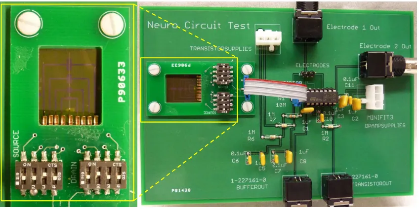
2-2: Flexible Pentacene Thin Film Transistors and Printed Circuit Board Design
Figure 2-1. (A) Schematic of the organic thin film transistor, a photographic example of which is seen in (B). (C) and (D) are the representative ID-VDS and ID-VGS properties of the devices,
respectively. The channel width is 1500 µm and length is 100 µm. These properties were measured in an inert nitrogen environment.
Pentacene thin film transistors (TFTs) were fabricated in bottom-gate, bottom-contact
configuration on a Kapton® substrate.18,19
A schematic of the device is illustrated in Figure 2-1(A).
Gold gate and source/drain contacts were patterned by photolithography with a thickness of 20
nm. A 500 nm parylene-C dielectric layer was deposited through physical vapor deposition. The
pentacene precursor was applied by spin-coating and then thermally converted to pentacene to
form the bottom-gate, bottom-contact configuration TFT. Figure 2-1(B) shows photograph of
-50 -40 -30 -20 -10
0
10
10
-1010
-910
-810
-710
-610
-5 VDS = - 50VV
GS(V)
I
D(
A
)
0 -10 -20 -30 -40 -50
0 -2 -4 -6 -8 -10 -12
- 20V - 30V
V
GS = - 50V
- 40V
I
D(
µ
A
)
V
DS(V)
(A)
(C)
(D)
pentacene
Kapton
®source
drain
gate
parylene
9
Figure 2-2. The dual PCB board design. The large board contains all elements of the circuit excluding the transistor: the amplifying resistor, low-pass power supply filters, output buffer and high-pass filter, and input/output components. The ribbon cable attaches the transistor to the rest of the circuit. The enlarged image on the left clearly shows the copper fingers used to make pressure contact with the organic TFT underneath.
the device electrodes before spin-coating the organic semiconductor. Representative device
characteristics measured under inert nitrogen environment are shown in Figure 2-1 (C) and
Figure 2-1 (D). Hole accumulation can be seen in the ID-VDS curve, characterized by linearity at
low absolute drain-source biases and saturation at large negative biases. The saturation mobility
is 0.123 ± 0.038 cm2
/(Vs), extracted from more than 50 transistors fabricated on different
samples. The on/off current ratio is about 105, as shown in ID-VGS curve [Figure 2-1 (D)]. The
pentacene TFTs were tested in both common source and common drain amplifier configurations.
A circuit consisting of all elements of the amplifying configurations except the transistor was
created using a custom printed circuit board (PCB), which is shown in Figure 2-2.
In order to make the electrical connection between the pentacene TFTs on a flexible
substrate and the PCB, the buried bottom gate had to be revealed. This was done by removing
10
selectively etched with oxygen plasma, while keeping the active area protected. An additional
small PCB with switches and finger-shaped beryllium copper contacts on the underside was
designed to make mechanical contact with the flexible substrate of the transistor array. By
clamping the small PCB onto the larger PCB with the flexible transistor array in between, the
beryllium copper fingers are able to make solid mechanical contact with the electrodes of the
transistor array, forming the electrical connection to the PCB. The pressure contact PCB is
highlighted in yellow and enlarged in Figure 2-2. A short ribbon cable was used to connect the
gate, source and drain of the organic transistor to their respective locations on the main PCB. The
circuit on the main PCB was designed to be used for either common source or common drain
amplifying circuits. Since the source and drain of the organic transistors are interchangeable,
switching between the two configurations was possible by changing power supply polarity. A
10MΩ resistor was connected to the drain or source of the organic transistor depending on the
desired circuit topology. This large resistance was used in order to yield higher gain. Power was
supplied the organic transistor amplifier through 0.14 Hz low-pass filters in order to reduce noise
coming from voltage supply electronics. The amplifier output was directly connected to a
unity-gain buffer in order to reduce loading by subsequent measurement equipment.
2-3: Organic Electronics for Sensors with Amplification
The common source amplifier configuration was tested with multiple pentacene TFTs on
the dual PCB setup. The source/drain transistor power supplies were kept at a difference of 50 V.
The maximum gain was 5.0 dB for the highest performance device, while the average gain was
2.3 dB. Figure 2-3 (A) shows a characteristic input/output voltage response for the best transistor
with a 100 µm channel. The source supply was +28 V and the drain supply was -22 V. The input
was a 1 Vpp 10 Hz sine wave. The output is inverted due to the common source topology. The
frequency response for the same organic transistor amplifier in the common source configuration
11
Figure 2-3. Results from common source amplifier using pentacene TFT showing the (A) representative output versus input and (B) bode plot. Both results shown were taken from the same 100 µm channel length device.
the transistor used. The square wave response rise and fall time of the amplifier was found to be
0.5 ms each.
The common drain topology was tested by reversing the polarity of the TFT power
supplies, effectively exchanging the source and drain. The maximum output of the device with a 1
Vpp input was 0.65 Vpp, or an attenuation of 3.7 dB. A frequency sweep revealed a 3dB
bandwidth of 2.8 kHz, much higher than the common source circuit, as expected.
To test the applicability of using organic electronic in sensing neural signal, a
pre-recorded human EEG data was sent as input with appropriate DC bias for amplification. In Figure
2-4, the output from organic sensor (red) is able to record most of input features from human
EEG data (blue), promising organic electronics for neural sensing.
2-4: Discussion and Conclusions
In addition to the gain of the common source amplifier using pentacene TFTs (between
2.3 dB and 5 dB), the preliminary bench test on recording human EEG suggest organic electronic
10
110
210
3-1
0
1
2
3
4
5
G
a
in
(
d
B
)
Frequency (Hz)
0
200
400
-1.0
-0.5
0.0
0.5
1.0
1.5
Am
p
li
tu
d
e
(
V
)
Time (ms)
Input Output
12
Figure 2-4. Organic electronic sensor for recording neural signal. (Blue) Pre-recorded human EEG signal, and (Red) measured output from organic electronic sensor. The output signal was inverted for clear comparison.
sensor is able to record neural signal in few mV amplitude. Current ECoG arrays use either
passive electrodes or common drain amplifiers with unity gain. Integrating any level of gain
directly at the electrode should improve the overall system performance. The attenuation seen in
the organic transistor in common drain configuration, 3.7 dB, would decrease the overall system
performance, but would still be acceptable for many neural signal acquisition tasks. The tradeoff
for increased gain is decreased bandwidth: ~800 Hz for the common source configuration versus
~2.8 kHz for the common drain configuration. Given that the majority of clinically relevant, cortical
surface brain activity occurs below 500 Hz,20
a bandwidth of 800 Hz would be sufficient for most
applications. However, developing multiplexed electrode arrays may be difficult, given the low
frequency response of the transistors.
One of the challenges faced while testing the amplifiers was the performance reduction of
the pentacene TFTs in ambient atmosphere. Devices were initially characterized directly after
fabrication, while still immersed in a pure nitrogen environment. The devices were subsequently
13
continuously decreased as a result of exposure to moisture and oxygen. Several different
encapsulating materials were applied to the TFTs in preliminary attempts to prevent this
degradation. None of the materials so far investigated effectively protected the devices from
reduction in their performance while exposed to air. There are several items remaining to be
addressed before organic transistors can be used to develop large arrays of multiplexed
electrodes. First, the noise performance of the organic transistor amplifiers will be evaluated to
insure sufficient signal to noise levels in the final system, while measuring neural signals of 1 mV
amplitude or less. Initial noise measurements appear promising. Second, the ability to pattern
hundreds of organic transistors on a single flexible substrate will need to be developed.
Prototypes of such devices have been fabricated, utilizing etching and deposition processes to
create vertical integration access (VIA) holes to connect individual transistors using multiple metal
layers. Finally, a new encapsulation system will need to be developed to fully protect the
transistors from exposure to air and biological fluids. New fabrication procedures and
encapsulation materials are being evaluated for their long term reliability.
The devices described in this chapter have been shown to work as amplifiers with
adequate gain and bandwidth required for clinical and research neural sensor applications. While
additional advancements are necessary, the potential advantages of organic µECoG electrode
14
2-5: References
(1) Campbell, P. K.; Jones, K. E.; Huber, R. J.; Horch, K. W.; Normann, R. a. A Silicon-Based, Three-Dimensional Neural Interface: Manufacturing Processes for an Intracortical Electrode Array. IEEE Trans. Biomed. Eng. 1991, 38, 758–768.
(2) Ryu, S. I.; Shenoy, K. V. Human Cortical Prostheses: Lost in Translation? Neurosurg. Focus 2009, 27, E5.
(3) Griffith, R. W.; Humphrey, D. R. Long-Term Gliosis around Chronically Implanted Platinum Electrodes in the Rhesus Macaque Motor Cortex. Neurosci. Lett. 2006, 406, 81–86.
(4) Polikov, V. S.; Tresco, P. A.; Reichert, W. M. Response of Brain Tissue to Chronically Implanted Neural Electrodes. J. Neurosci. Methods 2005, 148, 1–18.
(5) Chao, Z. C.; Nagasaka, Y.; Fujii, N. Long-Term Asynchronous Decoding of Arm Motion Using Electrocorticographic Signals in Monkeys. Front. Neuroeng. 2010, 3, 3.
(6) Yeager, J. D.; Phillips, D. J.; Rector, D. M.; Bahr, D. F. Characterization of Flexible ECoG Electrode Arrays for Chronic Recording in Awake Rats. J. Neurosci. Methods 2008, 173, 279–285.
(7) Leuthardt, E. C.; Gaona, C.; Sharma, M.; Szrama, N.; Roland, J.; Freudenberg, Z.; Solis, J.; Breshears, J.; Schalk, G. Using the Electrocorticographic Speech Network to Control a Brain–computer Interface in Humans. J. Neural Eng. 2011, 8, 036004.
(8) Brunner, P.; Ritaccio, A. L.; Emrich, J. F.; Bischof, H.; Schalk, G. Rapid Communication with a “P300” Matrix Speller Using Electrocorticographic Signals (ECoG). Front. Neurosci.
2011, 5, 5.
(9) Ball, T.; Nawrot, W.; Pistohl, T.; Aertsen, A.; Schulze-Bonhage, A.; Mehring, C. Towards an Implantable Brain-Machine Interface Based on Epicortical Field Potentials; Biomed. Tech. (Berlin), 2004; pp. 756–759.
(10) Kellis, S. S.; House, P. a; Thomson, K. E.; Brown, R.; Greger, B. Human Neocortical Electrical Activity Recorded on Nonpenetrating Microwire Arrays: Applicability for Neuroprostheses. Neurosurg. Focus 2009, 27, E9.
(11) Kellis, S.; Miller, K.; Thomson, K.; Brown, R.; House, P.; Greger, B. Decoding Spoken Words Using Local Field Potentials Recorded from the Cortical Surface. J. Neural Eng.
2010, 7, 056007.
(12) Stead, M.; Bower, M.; Brinkmann, B. H.; Lee, K.; Marsh, W. R.; Meyer, F. B.; Litt, B.; Van Gompel, J.; Worrell, G. a. Microseizures and the Spatiotemporal Scales of Human Partial Epilepsy. Brain 2010, 133, 2789–2797.
15
(14) Epilepsy & Neurosurgery Product Guide; Ad-Tech Medical Instrument Corporation, 2008; p. 32.
(15) Viventi, J.; Kim, D.-H.; Moss, J. D.; Kim, Y.-S.; Blanco, J. a; Annetta, N.; Hicks, A.; Xiao, J.; Huang, Y.; Callans, D. J.; et al. A Conformal, Bio-Interfaced Class of Silicon Electronics for Mapping Cardiac Electrophysiology. Sci. Transl. Med. 2010, 2, 24ra22.
(16) Klauk, H.; Halik, M.; Zschieschang, U.; Schmid, G.; Radlik, W.; Weber, W. High-Mobility Polymer Gate Dielectric Pentacene Thin Film Transistors. J. Appl. Phys. 2002, 92, 5259.
(17) Afzali, A.; Dimitrakopoulos, C. D.; Breen, T. L. High-Performance, Solution-Processed Organic Thin Film Transistors from a Novel Pentacene Precursor. J. Am. Chem. Soc.
2002, 124, 8812–8813.
(18) Saudari, S. R.; Lin, Y. J.; Lai, Y.; Kagan, C. R. Device Confi Gurations for Ambipolar Transport in Flexible , Pentacene Transistors. Adv. Mater. 2010, 22, 5063–5068.
(19) Saudari, S. R.; Frail, P. R.; Kagan, C. R. Ambipolar Transport in Solution-Deposited Pentacene Transistors Enhanced by Molecular Engineering of Device Contacts. Appl. Phys. Lett. 2009, 95, 023301.
Much of this chapter appears in print: Adapted with permission from D.K. Kim*, Y. Lai*, B.T. Diroll, C.B. Murray, C.R. Kagan, Nature Communications, 3 ,1216, 1-6 (2012) Copyright © 2012, Rights managed by Nature Publishing Group doi: 10.1038/ncomms2218
* Both authors contributed equally
16
CHAPTER 3 High-Performance Nanocrystal Transistors and Integrated
Circuits on Flexible Plastic
In this chapter, we report the first NCIC inverters, amplifiers, and ring oscillators
fabricated from high mobility CdSe FETs. We previously introduced high mobility CdSe
NC-FETs that operated at high voltages on rigid substrates, achieved through both strong coupling,
by introducing the compact ligand ammonium thiocyanate, and through doping, by thermal
diffusion of indium at mild temperatures.1
Thiocyanate is an environmentally benign and
non-corrosive ligand, allowing solution-deposition of NC devices on a variety of substrates, including
flexible plastic substrates, which we have previously demonstrated.2
This greatly expands the
applicability of these materials compared to other recently developed novel ligands. For example,
while excellent mobilities have been observed with molecular metal chalcogenide complexes,3,4
these NCs are dissolved in hydrazine, an extremely caustic solvent that is not compatible with
flexible plastics. In addition, since a wide range of flexible electronic applications are typically
powered by small thin-film batteries or radio frequency fields,5,6
it is necessary to show the
scalability of these colloidal inks to minimize energy consumption. We recently demonstrated
low-voltage operation of flexible colloidal nanowire FETs using thin Al2O3 as our robust, high
capacitance and low leakage gate dielectric material compatible with plastics.7
Here, we
demonstrate high-performance NC-FETs that operate at low-voltages on flexible plastics and
serve as the building blocks of complex integrated circuits, demonstrating this class of materials
as a viable flexible, electronic technology.
3-1: Flexible and Low-Voltage Nanocrystal Field-Effect Transistor
To fabricate flexible devices, we used either a 25 or 50 µm thick polyimide substrate and
covered the substrate with 30 nm of atomic layer deposited (ALD) Al2O3 at 250 o