Study of Effective Dielectric Permittivity and Capacitance
for Finite Dielectric Thickness Coplanar Waveguide
1
Shanu Sharma,
2Alok Kumar Rastogi
1,2Dept. of Physics & Electronics, Institute for Excellence in Higher Education, Bhopal, MP, India
Abstract
At higher frequencies microwave and millimeter wave transmission lines play an important role .Among all transmission lines CPW is rapidly becoming salient substitute due to its uniplanar geometry. In this paper simulation and Analysis (quasi static analysis using conformal mapping) of FCPW (Finite dielectric thickness Coplanar Waveguide) on Alumina and Roggers substrate with varying height of substrate are analyzed. The effect of Capacitance and effective permittivity on aspect ratio is also analyzed. Simulations are carried out on SONNET software; it is based upon Method of Moments principle and gives excellent simulations which are consistent with actual fabrications. This paper will help to optimize the design and fabrication of the FCPW for various dedicated applications.
Keywords
Coplanar Waveguide, Transmission Line, Quasi Static Analysis, Conformal Mapping, SONNET.
I. Introduction
In amplified use of hybrid, monolithic microwave and millimeter
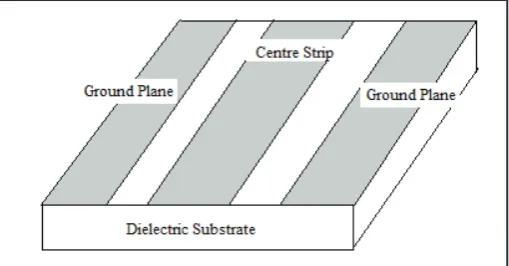
wave circuits the choice of transmission line is coplanar waveguide (CPW). It is the most striking alternative to conventional used microstrip line and stripline due to its uniplanar geometry. It consist of a centre strip with two ground planes located in the same plane [1-2] i.e., on the same surface of dielectric slab as shown in Figure.1. The ground plane being on the same surface lends itself to easy mounting of circuit elements and active devices; Drilling of holes or slots through the substrate is not needed [3-6]. CPW structures are commonly used in high-speed circuits and interconnect. It offers several advantages over microstrip which are summarized in Table 1. The use of CPW in the design of circuit components and transmission lines is not yet widespread. One reason for this is due to the lack of analytical data pertaining to the characteristics of CPW [7-8].
The electromagnetic wave carried by a coplanar waveguide exists to a certain extent in the dielectric substrate, and partly in the
air above it, electric and magnetic field distribution is shown in fig. 2.
Fig. 1: Conventional Coplanar Waveguide Structure
Fig. 2: Electric and Magnetic Field Distribution in CPW
Table 1: Comparison Between Microstrip line and CPW Properties Microstrip CPW
Dispersion High Low
Losses Low High
Coupling High Low
Design flexibility Low High
Circuit size Large Small
Via holes Yes No
In general, the dielectric constant of the substrate will be different than that of the air, so that the wave is travelling in an inhomogeneous medium [9-12]. As a consequence CPW will not support an exact TEM mode; at non-zero frequencies. At low frequencies, both loss and dispersion are limited and this mode is frequently called “quasi-TEM” mode because its propagation characteristics are similar to the TEM mode [13,18].
II. Materials and Methods
A. Alumina Substrate
Alumina is the ceramic form of sapphire. It has balanced properties of insulation, thermal conductivity and breaking strength. It is usually available in white color having dielectric constant varying
from 9.5 to 10 with loss tangent tanδ = 0.0002. Its unique property is surface roughness and excellent adhesion with a thin film and thick film metallization due to fine particles. Various advantages
of Alumina are: Physical and chemical properties are stable even at very high temperatures, High Mechanical strength, Good in insulation properties, Less porous with good smoothness. Gold metallization is frequently used with alumina. Usually a very thin adhesion layer is used between alumina and gold.
B. Roggers Substrate
This is Temperature Stable Microwave Laminates which are available in a wide range of dielectric constants. TMM (Thermoset Microwave Materials) are ceramic, hydrocarbon, polymer composites designed for high plated-thru-hole transmission line applications. The electrical and mechanical properties of TMM
laminates unite many of the benefits of both ceramic as well as
the specialized production techniques [15]. We have used TMM6 with dielectric constant equal to 6.0 ±0.080.
III. Quasi Static Analysis
A CPW can be quasi-statically analyzed by the use of conformal mapping. The closed form design equation obtained by conformal mapping method which is simplest and most often used method
consists of complete elliptic integral which are difficult to calculate
[1-2]. Thus approximate formulas are proposed for the calculation of elliptical integral by conformal mapping. For analysis of CPW
with finite dielectric substrate we have to assume capacitance
due to lower half plane is sum of free space and dielectric layer capacitance with permittivity ( ). Conformal Transformation is used to transform CPW into parallel plate structure [7-8]. The capacitance due to upper half plane is given by:
The transformation is:
and
Therefore Capacitance is given by:
Where k1, k2 are elliptical integrals The total capacitance is given by
We can also obtain by following equation:
Where filling factor ‘q’ is given by:
IV. Structure and Design
For practical applications it is impossible to take dielectric
substrate and ground planes to be infinite so CPW with finite dielectric substrate and finite width ground planes are required
for many practical applications [14]. The CPW analyzed in this
paper is Finite substrate thickness CPW as shown in fig. 3. In this
structure centre strip conductor with two ground planes on either side mounted on dielectric substrate with height of dielectric layer
taken as ‘h’ [1] [16].
Fig. 3: CPW with Finite Dielectric Substrate
In this study Height of substrate and gap between ground plane and centre strip is varied which is listed in Table 2 & 3 for Alumina and Roggers Substrate respectively. The effects of height of substrate and gap between strip and ground plane have also been analyzed.
Table 2: Dimensions of CPW with Alumina as Dielectric Substrate
S.
No. Height of Substrate(h) in mm Gap(g) in mm Width(w) in mm
1. h=0.4 0.15 0.28
0.3 1.02
2. h=0.28 0.15 0.32
0.3 1.47
3. h=0.19 0.150.3 0.422.2
Table 3: Dimensions of CPW with Roggers TMM1 as Dielectric Substrate
S. No. Height of Substrate(h) in
mm Gap(g) in mm Width(w) in mm
1. h=0.381 0.150.30 0.762.99
2. h=0.508 0.150.30 0.672.4
3. h=0762 0.15 0.62
0.30 1.84
V. Result and Discussion
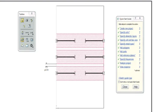
Fig. 4 (a) & (b) shows 2D & 3D model for FCPW respectively obtained through SONNET software simulation [17]. Simulation
is done on Alumina and Roggers substrate with εr =9.8, loss tangent tanδ = 0.0002 and εr =6.0, loss tangent tanδ = 0.0023
respectively. The simulated parametric study results and conformal mapping analysis for FCPW are obtained. Graph shown below represents the effect of aspect ratio and gap between strip and ground plane on capacitance, Effective dielectric permittivity,
transmission coefficient and reflection coefficient for varying
height of substrates.
Fig. 4: (b) 3-D model of FCPW
Fig. 5: (a) Variation of Capacitance with aspect ratio for varying height of Alumina Substrate
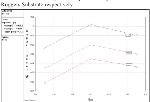
Fig. 5 (b): Variation of Capacitance With Aspect Ratio for Varying Height of Roggers Substrate
Fig. 5(a) and Fig. 5(b) shows the capacitance versus a/b for Alumina
and Roggers Substrate respectively. From figure it is clear that
the capacitance of FCPW is sensitive to change in aspect ratio. From quasi static analysis it is seen that Capacitance decreases with increasing a/b. And the slope of curve almost remains same for all heights. As height of the substrate increases, its capacitance decreases.
Fig. 6 (a) and 6 (b) shows the effective dielectric permittivity versus a/b for Alumina and Roggers substrate respectively. From
the graph it is clear that the effective dielectric permittivity (εeff) is
also sensitive to change in aspect ratio. From quasi static analysis
it is seen that εeff decreases with increasing a/b. And the slope of
curve almost remains same for all heights. As height of substrate increases effective dielectric permittivity decreases.
Fig. 6: (a)Variation of Effective Dielectric Permittivity With Aspect Ratio for Varying Height of Alumina Substrate
Fig. 6: (b) Variation of Effective Dielectric Permittivity with aspect ratio for varying height of Roggers Substrate
Fig. 7 (a) and (b) shows the Capacitance versus Gap for Alumina
and Roggers Substrate respectively and fig. 8 (a) and (b) shows
the effective dielectric permittivity versus Gap for Alumina and Roggers Substrate respectively.
Fig. 7: (b) Variation of Capacitance with gap (mm) for varying height of Roggers Substrate
Fig. 8: (a) Variation of Effective Dielectric Permittivity with gap (mm) for varying height of Alumina Substrate
Fig. 8: (b) Variation of Effective Dielectric Permittivity with gap (mm) for Varying Height of Roggers Substrate
From simulations it is seen that capacitance and effective dielectric permittivity changes with varying gap between strip and ground plane. Capacitance sequentially decreases for Alumina then for Roggers substrate while effective dielectric permittivity remains almost same with increasing gap between strip and ground plane for both substrates at all heights of substrate.
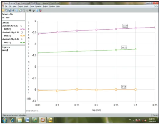
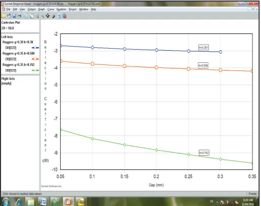
Fig. 9. (a) and (b) shows the Transmission coefficient versus Gap for Alumina and Roggers Substrate respectively and fig. 10 (a) and (b) shows the Reflection Coefficient versus Gap for Alumina and Roggers Substrate respectively. Reflection and transmission coefficients are also plotted through simulations. It is found that for Roggers, the transmission coefficient decreases with gap while
for alumina it increases and reflection coefficient varies almost
same for both the substrates.
Fig. 9: (a) Variation of Transmission Coefficient with gap (mm)
for varying height of Alumina Substrate
Fig. 9: (b) Variation of Transmission Coefficient with gap (mm)
for varying height of Roggers Substrate
Fig. 10: (a) Variation of Reflection Coefficient with gap (mm) for
Fig. 10: (b) Variation of Reflection Coefficient with gap (mm) for
varying height of Roggers Substrate
VI. Conclusion
This study reports the quasi static analysis and parametric study
of FCPW. Hence it is concluded that in the process of FCPW’s
fabrication special attention needs to be taken about height of substrate and gap. FCPW is modeled through simulation which shows that alumina favors sequential decrease of capacitance,
increase of transmission and decrease of reflection coefficient
for varying heights.
References
[1] Simons R. N.,“Coplanar waveguide circuits, components and systems”, John Wiley and Sons. Inc., 2001.
[2] Wen C.P., “Coplanar waveguide: A surface strip transmission line suitable for nonreciprocal gyromagnetic device applications”, IEEE Transactions on Microwave Theory and Techniques, 1969; Vol. 17, No. 12, pp. 1087–1090. [3] Mukesh kumar, Rohini Saxena, Anil Kumar, Pradyot Kala
and Reena Pant, “Theoretical Characterization of Coplanar Waveguide using Conformal Mapping”,International Journal of Advanced Research in Computer Science & Electronics Engineering, 2012; Vol-1, Issue-4, pp. 48-51.
[4] Md Saddam Hussain, Mukesh Kumar, Jaiswal A. K. And Rohini Saxena, “Dispersion and Characterization of Coplanar Waveguide Based on Conformal Mapping Technique”, Journal of Engineering Research and Applications (IJERA) ISSN: 2248-9622, 2013; Vol. 3, Issue 4, pp.1121-1125. [5] Kitazawa T., Hayashi Y. and Suzuki M., "A coplanar wave
guide with thick metal coating," IEEE Trans., 1976; Vol. MTT-24, pp. 604-608.
[6] Collin R. E., “Foundations for Microwave Engineering”, 2nd ed.New York: McGraw- Hill, 1992.
[7] Edwards T.C. and Steer M.B., “Foundations of Inter-connect and Microstrip Design”, John Wiley & Sons Ltd.
[8] Gupta K. C., Ramesh Garg and Bahl I. J., “Microstrip Lines and Slot Lines”, Artech House Inc. Washington, 1979. [9] Bhartia P. and Pramanick P., “A New Microstrip Dispersion
Model,'' IEEE Transactions on Microwave Theory and Techniques, 1984; Vol. 32, No. 10, pp. 1379-1384. [10] Min Wang, Bo Gao, Tian Yu, and Ling Tong, “Analysis of
Characteristics of Coplanar Waveguide with Finite Ground-planes by the Method of Lines” PIERS ONLINE, 2010; Vol. 6, No. 1.
[11] Ingo Wolff, “Coplanar Microwave Integrated Circuits”, VerlagsbuchhandlungDr.Wolff, GmbH. Published by John Wiley & Sons, Inc. Copyright © 2006.
[12] Kumar R.R., Aditya S., and Chadha D., "Dielectric loaded shielded edge coupled conductor backed coplanar waveguide structures," AEU (International J. of Electronics and Comm.), 1996; vol. 50, pp. 384 – 388
[13] Ghione G. and Naldi C. U.,‘‘Parameters of Coplanar Waveguides with Lower Ground Plane’’, Electron. Letter,
1983; Vol. 19, No. 18, pp. 734—735.
[14] Janiczak B. J., “Analysis of coplanar wave guide with finite
ground planes,” AEU, 1984; Vol. 38, no. 5, pp. 341-342. [15] Rogers Corporation, “Rogers Corporation: TMM Thermoset
Microwave Materials Data Sheet”, www.rogerscorp.com/.../ TMM-Thermoset-laminate-data-sheet-TMM3-TMM4-T MM6-TMM10-TMM10i.aspx.
[16] Gupta K. C., Garg R., Bahl I. J., Bhartia P., “Microstrip Lines and Slotlines”, 2nd ed.Artech House, Inc., 1996.
[17] High Frequency Electromagnetic Software SONNET-13.56 User guide.
[18] Weller T. M., Katehi L. P. B., Rebeiz G. M., ‘‘High Performance Microshield Line Components,’’ IEEE Trans. Microwave
Theory Tech., 1995; Vol. 43, No. 3, pp. 534—543.
Ms. Shanu Sharma,she is currently undertakingher research work (P.hD) from Barkatullah University, Bhopal under the guidance of Dr. Alok
Kumar Rastogi in field of microwave
communication.She has valuable experience of six years in teaching as a lecturer in Institute for Excellence in Higher Education, Bhopal. She didM.Sc. Electronics in 2008 and M.Sc. Mathematics in 2010 from Dr. Hari Singh Gour University, Sagar (M.P.). She has participated in many national and international conferences. She has published many research papers in reputed journals.
Dr. Alok Kumar Rastogi Presently Dr. Alok Kumar Rastogi is Professor & Head, Department of Physics & Electronics at Institute for Excellence in Higher Education Bhopal. He did M.Phil (Physics) from the Department of Physics & Astrophysics, University of Delhi in 1984 and completed his Ph.D. Degree in Electronics Engineering from Bhopal University, Bhopal in the year 1990. He received
Young Scientist Award for his excellent research work in the field
Minor Research Projects awarded by UGC, New Delhi. UGC New Delhi awarded him several research projects to carry out
research work in the field of microwave communication. He is having professional affiliation with various national organizations.
He is Fellow of IETE and life member of IE, IAPT, ISCA, ISTE, PSSI etc. Seven Ph.D. have been awarded under his supervision
in the field of microwave communication and five candidates are