e-ISSN: 2278-067X, p-ISSN: 2278-800X, www.ijerd.com
Volume
10
, Issue
3
(March 2014), PP.51-58
IC Interconnects Modeling using X-parameters
Nick K. H. Huang
1, Li Jun Jiang
21,2Department of Electrical and Electronic Engineering, The University of Hong Kong, Pokfulam HKSAR.
Abstract:-The performance of IC interconnects has been stretched tremendously recently years by high speed integrated circuit systems. Even though S-parameters are popularly used for the characterization of IC interconnects, their modeling has to consider the existence of active devices, such as buffers and drivers. The I/O model is difficult to obtain due to the IP protection and limited information. In this paper, we propose to use the X-parameter to model the IC interconnect system. Based on the PHD formalism, X-parameter models provide an accurate frequency-domain method under large-signal operating points to characterize their nonlinear behaviors. Another challenge is that in the digital IC system, the digital signal is best represented in the time domain while S-parameter and X-parameter are both in the frequency domain. Hence, a proper control of the harmonic contents inside the input signal to drivers and buffers are needed. Starting from modeling the CMOS inverter, we present the whole link modeling primarily based on X-parameter for the pulsed digital signal. According to our knowledge, this is the first time X-parameter is applied for this type of applications.
Keywords:-Buffer; nonlinearity; polyharmonic distortion; digital pulse signal; X-parameters.
I.
INTRODUCTION
Over past decades, the signal speed of modern integrated circuits (IC) has spiked to gigahertz level. Consequently, the working bandwidth is significantly expanded. Unlike analog amplifiers, buffers and drivers, implemented by the CMOS technology, work under the extreme nonlinear mode. They show strong pull-up and push-down IO behaviors. Therefore, the famous IBIS model is able to become a popular facility to serve as the behavior model of the IC IOs. However, IBIS models are based on the I-V curve measurements. They lack the parasitic coupling information and are found that it does not work well for high speed signals in the digital system.
For the high speed system, the network parameter S-parameter is used to characterize the frequency response of passive parasitic structures, such as IC interconnects, packaging, etc. However, it is not good for digital devices because S-parameter is only good for linear devices. Devices in IC circuits, such as buffers or drivers, demonstrate extreme nonlinearity. To accurately model digital devices, one way is to use the accurate SPICE model. However, it is not trivial to obtain the SPICE model, especially when the working frequency is high. Meanwhile, it is preferred in industries to maintain the IP privacy as much as possible. Hence, this makes it even more difficult to find the proper SPICE model of the device. The behavior model is not considered to be intrinsic because it involves too many approximations. A better nonlinear device modeling technique is needed.
X-parameter is a new technology developed by Root and Wood [1] for the characterization of nonlinear devices. Mathematically S-parameter can be considered as the special linear case of X-parameter. It was first introduced from the polyharmonic distortion (PHD) modeling [2, 3]. It is not only suitable to existing nonlinear simulation methods, but also can be measured through commercial nonlinear vector network analyzers. It makes the conventional linear black box into the nonlinear black box. It has been applied for analog devices in communication systems. However, there are very limited trials for using X-parameter technologies in the digital circuits. Its practical trial for the signal integrity analysis is rare. In [4], the X-parameter was first experimented for the high speed link I/O modeling. However, it uses the sinusoidal signal as the input signal that is very different from digital signals being used in practical IC system. However, it is not trivial to add a DC pulse sequence signal into the input of X-parameter simulation link because the spectrum of the input signal will be much more complicated than the sinusoidal one. However, to analyze the cross talk and noise coupling mechanism, it is necessary to apply the real digital signal into the system. From [5], X-parameter models showed a great agreement with analog LNA with pulse input signals for the first time. We continue to advance the work to investigate the X-parameter behaviors.
modeling with realistic digital signal inputs. Therefore, it provides the first look at the performance of X-parameters for IC signal integrity modelling.
The remainder of this paper is organized as follows. The PHD models represented along with X-parameters are introduced first. Next, the methodologies of building X-parameter models and processing pulse signals for X-parameter simulations are presented. Then, simulation studies using the representative digital CMOS inverter and buffer for IC interconnect link are given and discussed to demonstrate the performance of X-parameter models for pulse signals in signal integrity.
II.
PHD
AND
X-PARAMETER
FORMULATIONS
The basic concept of X-parameters is proposed on the PHD model, which is based on the principle of harmonic superposition and the nonanalytic property of the spectrum mapping function of the nonlinear system. It can be treated as the nonlinear extension of the linear S-parameter [2]. It intends to implement a frequency domain black box modeling approach. Assume the nonlinear circuit has N signal ports. The incident wave with the frequency harmonic index l at port q can be defined as Aql while the scattered wave with the frequency
harmonic index k at port p can be defined as Bpk. Then the spectrum mapping function of the nonlinear system
from all input frequency contents of all signal ports to the single scattered wave at the signal port p with the frequency k is.
𝑩𝒑𝒌= 𝑭𝒑𝒌 𝑨𝟏𝟏, 𝑨𝟏𝟐, … , 𝑨𝟐𝟏, 𝑨𝟐𝟐, … , 𝑨𝑵𝟏, 𝑨𝑵𝟐, … (1)
Then the A-wave can be defined using S-parameter type concept as
𝑨𝒒𝒍=
𝑽𝒒𝒍+ 𝒁𝒄𝒒𝒍𝑰𝒒𝒍
𝟐 (2)
𝑩𝒑𝒌=
𝑽𝒑𝒌+ 𝒁𝒄𝒑𝒌𝑰𝒑𝒌
𝟐 (3)
Then based on the harmonic superposition, the scattered B wave can be generally represented by A11, Aql and the
conjugate of Aql:
𝑩𝒑𝒌 𝑨𝟏𝟏, 𝒇 = 𝑿𝒑𝒌
𝑭𝑩 𝑨
𝟏𝟏, 𝒇 ∙ 𝑷𝒌
(4)
+ 𝑿𝒑𝒒,𝒌𝒍(𝑺) 𝑨𝟏𝟏, 𝒇 ∙ 𝑷𝒌−𝒍∙ 𝑨𝒒𝒍 𝒍=𝑴
𝒍=𝟏 𝒒=𝑵
𝒒=𝟏
+ 𝑿𝒑𝒒,𝒌𝒍(𝑻) 𝑨𝟏𝟏, 𝒇 ∙ 𝑷𝒌+𝒍∙ 𝑨𝒒𝒍∗ 𝒍=𝑴
𝒍=𝟏 𝒒=𝑵
𝒒=𝟏
Because the phase term is only referred to the fundamental frequency,
𝑿𝒑𝟏,𝒌𝟏(𝑺,𝑻) = 𝟎 (5)
In above formulation, P is the phase term of the fundamental frequency.
𝑷 = 𝒆𝒋𝑨𝒓𝒈(𝑨𝟏𝟏) (6)
𝑋𝑝𝑞 ,𝑘𝑙(𝑆) is a scattering parameter that accounts for the contribution to the kth harmonic at port p due to the lth
harmonic of the incident wave in port q. It is very much similar to the conventional concept of S-parameter
except that it supports the relationship between different harmonic frequencies. 𝑋𝑝𝑞 ,𝑘𝑙(𝑇) is a new type of scattering parameter that accounts for the contribution to the kth harmonic at port p due to the lthharmonic of the conjugated incident wave in port q. It is very unique to PHD method. It accounts the impact of the phase from high order harmonic inputs. In (6), P is a pure phase along with the magnitude-only dependence on A11 by convention [2].
The S and T functions describe a full set of parameters to completely characterize the nonlinearities.
III.
X-PARAMETER
MODELING
FOR
IC
INTERCONNECTS
buffers in the system are of strong linearity. Hence, X-parameter will be used to model them. To illustrate the proposed method clearly, we exclusively use ADS in this paper, including the X-parameter extraction of the device.
A. Input Signals
The first step is to extract the X-parameter of the device. It is convenient to extract the X-parameter model from a given SPICE model of the device in ADS. However, one issue is critical: what are the fundamental frequency and its harmonics? It is related to the setup of M in equation (4).
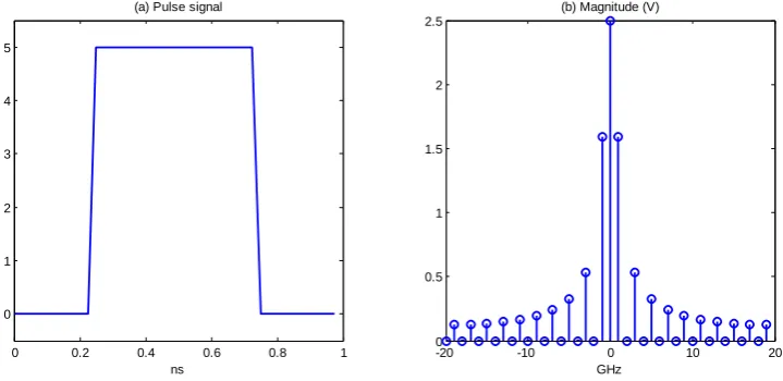
If the input signal is sinusoidal, the input setup is trivial. However, if the input is a practical periodic pulsed digital signal as shown in the left figure of Fig. 1, there are many spectrum contents being input into the device and thereby the X-parameter model during its application. An example of the rich spectrum content is shown in the right figure of Fig. 1. It shall be noted that there is a very strong DC component in the spectrum due to the fact that the given pulse signal swings between 0 Volt and 5 Volt in this example.
Fig. 1:Input pulse signal in (a) the time domain and (b) the frequency domain.
If the pulse signal has zero rise and fall times, the wide of the signal is τ and the period of the pulse sequence is T, its Fourier series expansion is
𝒔 𝒕 = 𝒗𝟎 𝝉 𝑻+ 𝒗𝟎
𝟐 𝒏𝝅𝐬𝐢𝐧
𝝅𝒏𝝉 𝑻 𝐜𝐨𝐬
𝟐𝝅𝒏
𝑻 𝒕
∞
𝒏=𝟏
(7)
Obviously the spectrum contents are discrete with a DC term that is directly determined by the space ration of the pulse signal. All spectrum contents are in the harmonic position of ω0=2π/T. For digital circuits, every bit
contains the same width. Therefore, τ = 0.5T. Equation 7 becomes
𝒇 𝒕 = 𝝉
𝑻+
𝟐 𝒏𝝅𝐬𝐢𝐧
𝝅
𝟐𝒏 𝐜𝐨𝐬 𝛚𝟎𝒏𝒕 ∞
𝒏=𝟏
=𝝉
𝑻+
𝟐
𝟐𝒎 + 𝟏 𝝅 −𝟏
𝒎𝐜𝐨𝐬 𝟐𝒎 + 𝟏 𝛚
𝟎𝒕 ∞
𝒎=𝟎 (8)
Several important features can be obtained from the above equation. First, the spectrum contents only have odd harmonics of the fundamental frequency. Even harmonics are all zeros. Meanwhile, the magnitude of all harmonics is inversely proportional to its order number. If we check the first 4 nonzero harmonics starting from the fundamental one, the magnitudes are
𝟐 𝝅,
𝟐 𝟑𝝅,
𝟐 𝟓𝝅,
𝟐 𝟕𝝅, …
Apparently the fundamental frequency is significantly larger than all other high order harmonics. This satisfies the critical preliminary requirement that the harmonic superposition is being used by the X-parameter. Hence, it works to use X-parameter to model the pulsed input signal in the IC interconnect.
Because the number of harmonics could be infinite, another question is how to decide its truncation number. There comes the knee frequency in the CMOS technology. In reality, the pulsed signals in the digital signal can only have nonzero rise time. By calculating its spectrum, it can be seen that after certain frequency, the signal power of the digital signal spectrum begins to drop dramatically faster than 20 dB/decade. This
0 0.2 0.4 0.6 0.8 1 0
1 2 3 4 5
(a) Pulse signal
ns
-20 -10 0 10 20
0 0.5 1 1.5 2 2.5
(b) Magnitude (V)
turning point is defined as the knee frequency. It is a proper frequency above which spectrum in the signal spectrum can be ignored without causing many errors in most analyses.
If the 10% to 90% rising time of the digital signal is defined as t10-90, the empirical equation of the knee
frequency is
𝒇𝒌𝒏𝒆𝒆= 𝟎. 𝟑𝟓
𝒕𝟏𝟎−𝟗𝟎
(9)
Because today's digital signals require to transmit data at multi-gigabit rates, the rise time is assumed to be the nano or pico second scale. The faster the rise time is, the higher the knee frequency is. Hence, more significant high frequency terms need to be preserved. If we assume the rise time of the pulse signal in Fig. 8 is 25 ps, the knee frequency is about 14 GHz. Hence, it is necessary to employ 14 harmonics to represent the pulse signal propagating in the IC interconnect system.
B. X-Parameter Extraction and Simulation
With the known information of input signals, the X-parameter models of the device can be extracted accordingly. Agilent ADS can be used to obtain X-parameters if the device SPICE model is available.
It has to be noted that the X-parameter model in ADS only accepts power input sources. Hence, the pulse signal being used for digital IC interconnects cannot be directly used for the X-parameter extraction. To solve this issue, the Fourier transform is applied on the periodic pulse signal first. Using the harmonic truncation principle mentioned in the previous section, a sequence of power input sources based on the spectral components of the pulse signal is selected and composed. Then they are treated as the X-parameter generation source, which is corresponding Aql in equation 4.
The generated X-parameter model is then used in the harmonic balance simulation process for nonlinear circuits. The harmonic contents of input pulsed signals are employed again. It is critical to know that not only the magnitude but also the phase of each harmonic is needed in both X-parameter extraction and the harmonic balance simulation.
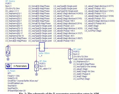
The output of the nonlinear simulation is a series of harmonic spectrum components. Inverse Fourier transform is utilized to recover the time domain waveform.The schematic of one of the examples for the X-parameter model generation is demonstrated in Fig. 2. This process is graphically shown in Fig. 3.
Fig. 3: The X-parameter simulation process for pulse signals.
C. CMOS Inverter and Buffer
The CMOS technology is popularly used in today's IC devices. The CMOS inverter is the most fundamental device. In this paper, we employ the 0.18 µm technology to construct the inverter. Later it will be used to build the CMOS buffer. To validate the inverter, 1-GHz fundamental frequency in the Harmonic Balance simulator was implemented.
The generation of the X-parameter model for the CMOS inverter follows the same procedure as described previously. The input pulse signal and its spectral components are shown in Fig. 1 for both time and frequency domains. The pulse signal is designed to have a 5-Volt amplitude. The average magnitude DC point is observed at 2.5 voltages.
If the fundamental frequency is 1-GHz, different number of harmonics inputted into the X-parameter model of the inverter will generate different output. After recovering the time domain wave form, it becomes obvious that more input harmonics will generate better output waveform. Meanwhile, if the harmonic balance simulation is applied on the inverter's SPICE model directly, the output can be employed as the reference. Fig. 4 depicts the output from X-parameter model using 1, 5, 10, and 20 input harmonics for the inverter and their comparisons with the direct SPICE model simulation result (in Green dash lines). It is observed that within the number of truncated harmonic numbers, the X-parameter model can generate the same output as that of the SPICE model. With increasing number of harmonics, the waveform migrates gradually to a smoother waveform in the time domain to reduce the Gibbs phenomena.
The CMOS buffer is composed of a couple of identical CMOS inverters. Using the 0.8 µm CMOS technology mentioned before, a buffer can be easily constructed in the simulator. A 1-GHz large signal was first used to excite the CMOS buffer at the fundamental frequency. Small signal tones are then sent to the input port at the harmonic frequencies of the fundamental. Next, the output waveforms of the buffer with 5, 10, 14, and 20 harmonic inputs given in Fig. 5 illustrate the comparison with the direct buffer model.
Fig. 4:DC + 1, 5, 10, and 20 Harmonic signals of CMOS inverter with 1 GHz fundamental frequency.
Fig. 5:DC + 5, 10, 14, and 20 Harmonic signals of CMOS buffer with 1 GHz fundamental frequency.
0 0.2 0.4 0.6 0.8 1
-1 0 1 2 3 4 5 6
1-Harmonic Signal at 1 GHz fundamental frequency
time (ns) v o lt a g e ( V )
0 0.2 0.4 0.6 0.8 1
-1 0 1 2 3 4 5 6
5-Harmonic Signals at 1 GHz fundamental frequency
time (ns) v o lt a g e ( V )
0 0.2 0.4 0.6 0.8 1
-1 0 1 2 3 4 5 6
10-Harmonic Signals at 1 GHz fundamental frequency
time (ns) v o lt a g e ( V )
0 0.2 0.4 0.6 0.8 1
-1 0 1 2 3 4 5 6 7
20-Harmonic Signals at 1 GHz fundamental frequency
time (ns) v o lt a g e ( V ) Vin Vout Inverter Vout X-model
0 0.2 0.4 0.6 0.8 1
-1 0 1 2 3 4 5 6
5 Harmonics Signals at 1 GHz fundamental frequency
time (ns) v o lt a g e ( V )
0 0.2 0.4 0.6 0.8 1
-1 0 1 2 3 4 5 6
10 Harmonics Signals at 1 GHz fundamental frequency
time (ns) v o lt a g e ( V )
0 0.2 0.4 0.6 0.8 1
-1 0 1 2 3 4 5 6
14 Harmonics Signals at 1 GHz fundamental frequency
time (ns) v o lt a g e ( V )
0 0.2 0.4 0.6 0.8 1
-1 0 1 2 3 4 5 6
20 Harmonics Signals at 1 GHz fundamental frequency
D. Transmission line with Buffer
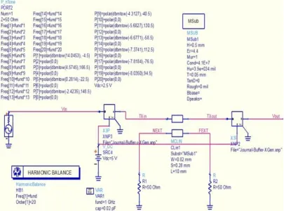
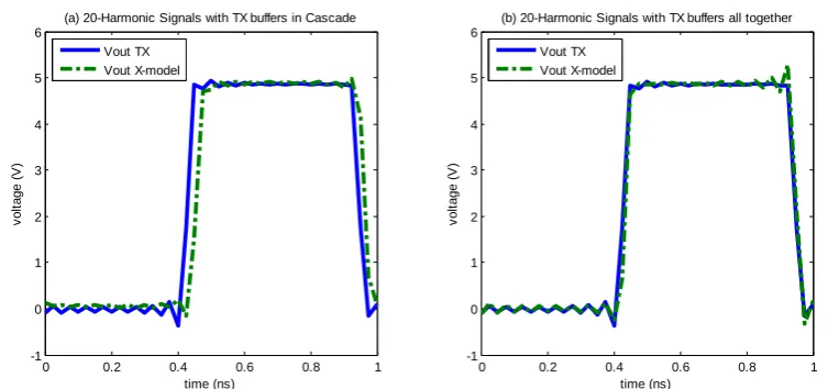
Next, we can cascade the buffers together with transmission lines to form a complete IC interconnect link. The harmonic balance is used as the simulation method. The buffers are represented by the X-parameter. The transmission lines are modeled by the transmission line model. Fig. 6 shows the two buffers cascaded with a transmission line in-between. We want to test the buffer's functionality along with the near and far end crosstalk on the other transmission line. The results of using the direct solver and X-parameter models are shown in Fig. 7 (a), and a significant delay is observed on the voltage output between them. This delay is due to a systematic issue in ADS. It uses the interpolation to generate output spectrum from X-parameter blocks in ADS. Although the input spectrum of first stage is exactly the same with it in xnp generation,the output spectrum is changed. Therefore, with single point xnp, the output of second stage may have several degree phase differences compared to real circuit. With more stages of cascade, the phase error is also increased [7]. In this case, because there is only one input data of original xnp, ADS does not have much information for interpolation. This causes the phase error.
In order to reduce the delay, another way we tried is to use the whole subcircuit as one X-parameter model. The other validation uses the whole setup shown in Fig. 6 all together as one X-parameter model. This reduces the flexibility of X-parameter usage since this X-parameter can be only used for this circuit or structure on purpose. The voltage output of direct solver and X-parameter model are shown in Fig. 7 (b). Clearly we see no time difference issue except a small glitch on the edge for the X-parameter model. As a result, there is a phase interpolation error in the ADS simulation.
Fig. 6:The schematic of the transmission line with buffers in ADS.
IV.
CONCLUSIONS
Fig. 7:DC + 20 Harmonic signals of CMOS buffers with transmission line at 1 GHz fundamental frequency. (a) X-parameters models in cascade. (b) Circuits all together as one X-parameter model.
ACKNOWLEDGMENT
This work was supported by Huawei Technologies Co., LTD. The authors also thank Agilent Technologies Inc. for providing the ADS X-parameter generation platform. We especially thank Jason Chen from Agilent EEsof EDA for the discussion.
REFERENCES
[1]. J. Wood and D. E. Root. Fundamental of Nonlinear Behavioral Modeling for RF and Microwave
Design. Norwood, MA: Artech House, 2005.
[2]. D.E. Root, J. Verspecht, D. Sharrit, J. Wood, and A. Cognata. Broad-band poly-harmonic distortion (PHD) behavioral models from fast automated simulations and large-signal vectorial network measurements. Microwave Theory and Techniques, IEEE Transactions on, 53(11):3656-3664, Nov. 2005.
[3]. Verspecht and D.E. Root. Polyharmonic distortion modeling.Microwave Magazine, IEEE, 7(3):44-57, June 2006.
[4]. J.E. Schutt-Aine, P. Milosevic, and W.T. Beyene. Modeling and simulation of high speed I/O links using X parameters. In Electrical Performance of Electronic Packaging and System (EPEPS), 2010
IEEE 19th Conference on, pages 29-32, Oct. 2010.
[5]. Nick K. H. Huang and Lijun Jiang. Simulation of pulse signals with X-parameters. In Electrical
Performance of Electronic Packaging and System (EPEPS), 2011 IEEE 20th Conference on, pages
129-132, Oct. 2011.
[6]. Agilent Advanced Design System. Version 2011.10. Copyright© 1983-2011. Agilent Technologies. [7]. Jason Chen. ADS email exchange, January 2014.
0 0.2 0.4 0.6 0.8 1 -1
0 1 2 3 4 5 6
(a) 20-Harmonic Signals with TX buffers in Cascade
time (ns)
v
o
lt
a
g
e
(
V
)
Vout TX Vout X-model
0 0.2 0.4 0.6 0.8 1 -1
0 1 2 3 4 5 6
(b) 20-Harmonic Signals with TX buffers all together
time (ns)
v
o
lt
a
g
e
(
V
)