Volume 1, Issue 5 (September2012) PP: 47-55
Voltage Sag and Mitigation Using Algorithm for Dynamic
Voltage Restorer by PQR Transformation Theory
Prof. Shivanagouda B. Patil
1, Dr. Shekhappa. G. Ankaliki
21E & E Engineering Department, Hirasugar Institute of Technology, Nidasoshi-591 236, Karnataka, India. 2E & E Engineering Department, SDM College of Engineering & Technology, Dharwad-580 002, Karnataka,
India.
Abstract––Voltage sag is one of the power quality issue and Dynamic Voltage Restorer (DVR) is used for mitigation of voltage sag. Voltage sag is sudden reduction in voltage from nominal value, occurs in a short time which can cause damage and loss of production in industrial sector. In this paper, focus is given only on DVR using an algorithm and the related implementations to control static series compensators (SSCs). Directly sensed three-phase voltages are transformed to p-q-r co-ordinates without time delay. The controlled variables in p-q-r co-ordinates has better steady state and dynamic performance and then inversely transformed to the original a-b-c co-ordinates without time delay, generating control signals to SSCs. The control algorithm is used in DVR system. The simulated results are verified and mitigation of sag is presented in this paper.
Key words––Voltage Sag, Static Series Compensator (SSCs), PQR Transformation, Dynamic Voltage Restorer (DVR)
I.
INTRODUCTION
In many recent years, power quality disturbances become most issue which makes many researchers interested to find the best solutions to solve it. There are various types of power quality disturbances in which voltage sag, voltage swell and interruption. This paper introduces DVR and its operating principle for the sensitive loads. Simple control based SPWM technique and „pqr‟ transformation theory [1] is used in algorithm to compensate voltage sags/swells. A scope of work is DVR system will be simulated by using Matlab/Simulink tool box and results were presented. Due to the increasing of new technology, a lot of devices had been created and developed for mitigation of voltage sag. Voltage sag is widely recognized as one of the most important power quality disturbances [2]. Voltage sag is a short reduction in rms voltage from nominal voltage, happened in a short duration, about 10ms to seconds. The IEC 61000-4-30 defines the voltage sag (dip) as a temporary reduction of the voltage at a point of the electrical system below a threshold [3]. According to IEEE Standard 1159-1995, defines voltage sags as an rms variation with a magnitude between 10% and 90% of nominal voltage and duration between 0.5cycles and one minute [4] & [5]. Voltage sag is happened at the adjacent feeder with unhealthy feeder. This unhealthy feeder always caused by two factors which are short circuits due to faults in power system networks and starting motor which draw very high lagging current. Both of these factors are the main factor creating voltage sag as power quality problem in power system. Voltage sags are the most common power disturbance which certainly gives affecting especially in industrial and large commercial customers such as the damage of the sensitivity equipments and loss of daily productions and finances. An example of the sensitivity equipments are programmable logic controller (PLC), adjustable speed drive (ASD) and chiller control. There are many ways in order to mitigate voltage sag problem. One of them is minimizing short circuits caused by utility directly which can be done such as with avoid feeder or cable overloading by correct configuration. The control of the compensation voltages in DVR based on dqo algorithm is discussed in [6]. DVR is a power electronic controller that can protect sensitive loads from disturbances in supply system. Dynamic voltage restorers (DVR) can provide the most commercial solution to mitigation voltage sag by injecting voltage as well as power into the system. The mitigation capability of these devices is mainly influenced by the maximum load; power factor and maximum voltage dip to be compensated [7]. In [12-17] Voltage Sag Mitigation Using Dynamic Voltage Restorer System are discussed under fault condition and dynamic conditions.
II.
DVR SYSTEM
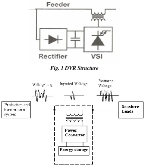
passive reactive components. The real power exchanged at the DVR output ac terminals is provided by the DVR input dc terminal by an external energy source or energy storage system. DVR structure comprises rectifier, inverter, filter and coupling transformer shown in Fig.1. Besides, pulse width modulated (PWM) technique is using to control variable voltage. Filter is using for elimination harmonic generated from high switching frequency in PWM technique. In power system network, DVR system is connected in series with the distribution feeder that supplies a sensitive load shown in Fig. 2. There are two main factors relating to the capability and performance of DVR working against voltage sags in a certain power system: the sag severity level and the Total Harmonic Distortion (THD). Both of these in turn are mainly decided by the DC source [9]
Fig. 1 DVR Structure
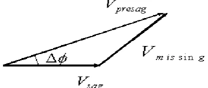
Fig. 2 DVR System in Power System
The Principle Operation of DVR System
In normal situation without short circuit in power system, a capacitor between rectifier and inverter (Fig. 1) will be charging. When voltage sag happened, this capacitor will discharge to maintain load voltage supply. Nominal voltage will be compared with voltage sag in order to get a difference voltage that will be injected by DVR system to maintain load voltage supply. PWM technique is using to control this variable voltage. In order to maintain load voltage supply, reactive power must be injected by DVR system. Practically, the capability of injection voltage by DVR system is 50% of nominal voltage. It is sufficient for mitigation voltage sag because from statistic shown that many voltage sag cases in power system involving less than 0.5 p.u. voltage drop.
Mathematical Model for Voltage Sag Calculation
F
s F
E
I
Z
Z
(1)sag F F
V
I Z
(2)1 1
tan
Ftan
S FF S F
X
X
X
R
R
R
(3)Where
S S S
Z
R
jX
, is the source impedance,Z
F
R
F
jX
F, is the impedance between the PCC and the fault, and1 .
E
p u
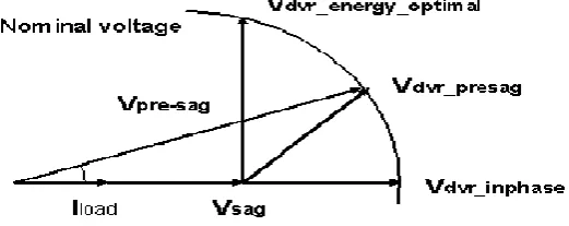
is the source voltage. The missing voltage which is the voltage difference between pre-sag condition and sagged (faulted) condition which is given by equation (4) and vectorial representation is shown in Fig. 4.sin
mis g presag sag
V
V
V
(4)Fig. 4 Vector Diagram Showing Voltage Sag
The missing voltage has to be provided by sag compensating device like Dynamic Voltage Restorer (DVR) which is injected in series with the supply voltages to bring the voltages to pre-sag condition.
.
III.
PROPOSED APPROACH
The objective of this paper is to implement DVR in series with a sensitive load. It is a series compensating device which injects a set of controllable three-phase AC output voltages, in series and synchronism with the distribution feeder voltages.The DVR employs solid state switching devices in a pulse width modulated inverter (PWMI), the magnitude and phase angle of the injecting voltages can be controlled independently. In this work directly sensed three phase voltages are transformed to p-q-r co-ordinates without time delay [1]. The controlled variables p-q-r co-ordinates have better steady state and dynamic performance. Later these are inversely transformed to the original a-b-c co-ordinates without time delay. It must able to respond quickly and experience no voltage sags to the end users of sensitive equipment shown in Fig. 3.
IV.
BASIC CONTROL STRATEGIES OF DVR
The type of the control strategy mainly depends upon the type of the sensitive or critical load, i.e. it depends on the sensitivity of the load to changes in magnitude, phase shift and wave shape of the voltage wave form. The control techniques adopted should consider the limitations of the DVR like voltage injection capability and energy limit. Voltage sag compensation can be done by DVR using real and reactive power transfer. Reactive power solely will not meet the requirements of dynamic compensation of disturbances that require real power transfer.
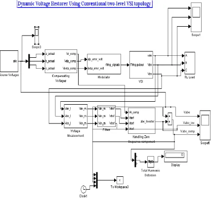
The three basic control strategies are, a) Pre-sag Compensation b) In-phase Compensation c) Energy Optimal Compensation
a) Pre-sag Compensation
Fig. 5 Vector Diagram of Pre-sag Compensation
b) In-phase Compensation
In this method, the restored voltages are in-phase with the depressed source side voltages regardless of load current and presag voltages, thus minimizing the magnitude of the injected voltage. Fig.4 shows phase compensation is not provided but has got better performance in compensating a broader range of voltage sags. The vector diagram for inphase compensation is shown in Fig. 6.
Fig. 6 Vector Diagram for Inphase Compensation
c) Energy Optimal Compensation
Voltages are injected at an angle that will minimize the use of real power since voltage restoration is the only requirement. That means the DVR voltage is injected perpendicular to the load current but the current will change the phase according to the new voltage applied to it and energy will be drawn from DVR. The vector diagram for optimal compensation is shown in Fig.7.
values. The controller in p-q-r domain is very simple and clear, has better dynamic and steady state performance than conventional controllers. The algorithm based on PQR power theory is used to get the reference compensation voltages in p-q-r domain and transformed back to 0
domain to drive the space vector modulator to generate the firing signals for inverter.PQR Transformation Theory
The 3-phase voltages of three-phase a-b-c coordinates can be transformed to
o
coordinates as given below, c b a o V V V V V V 2 3 2 3 0 2 1 2 1 1 2 1 2 1 2 1 3 2 (5)
If sinusoidal balanced voltages
v
aREF ,v
bREF andv
cREF are selected for the reference waves in the a-b-c coordinates, the reference waves ino
coordinates can be calculated and shown below,1 1
1
2 2 2
3 3 3
0 2 2 aREF REF REF bREF REF cREF v v V v v v (6)
Since the reference waves
v
aREF ,v
bREF andv
cREF are sinusoidal balanced, the 0-axis component voltagev
oREFdoes not exist and the reference wave
v
REF v
REF become sinusoidal and orthogonal on the
plane.Using the reference waves
v
REF v
REF in theo
coordinates in a mapping matrix, the voltages ino
coordinates can be transformed to p-q-r coordinates as given by (2).0
0
1
0
0
REF REF REF REF p o REF REF q REF REF r
v
v
v
v
v
v
v
v
v
v
v
v
v
v
(7) Where 2 2REF REF REF
v
v
v
(8)Combining (5) and (7) the voltages in a-b-c coordinates can be transformed to p-q-r coordinates as shown below,
Where
C
C C
1 22
0
0
1 0 0
REF REF REF REF REF REF REF REF v v v v v v C v v (10)
From p-q-r domain to a-b-c domain can be achieved by taking inverse of C,
1 p a b q c r v vv C v
v v (11)
Where
C
1
(
C C
1 2)
1
C C
21 111 1
1
1 0
2
2 1 1 3
3 2 2 2
1 1 3
2 2 2 C (12) 1 2
0
0
1
0
0
REF REF REF REF REF REF REF REFv
v
C
v
v
v
v
v
v
(13) PQR TransformationFig. 8 Physical Meaning of PQR Transformation
DVR Model Description
The block diagram of overall control flow is shown in Fig. 9. Here open loop feed forward control technique is adopted. Upon the occurrence of sag, there is a reduction in the phase voltages on the downstream of the DVR. The data is acquired by data acquisition system and detected. The speed with which the sag is detected depends upon the sensors and sag detection algorithms. Then the three phase voltages are processed using PQR algorithm. The reference compensating voltages are generated in PQR domain and transformed back to alpha-beta domain. The alpha and beta axis reference voltages are given as inputs to drive the space vector modulator. The generated firing pulses are used to fire the switches of the voltage Source Inverter (VSI). The topology of the VSI used is conventional 2-level, three-leg inverter and three-level (multi-level configuration) diode clamped inverter. Depending upon the topology of the inverter, the number of firing pulses may be 6/12.
Fig. 9 Simulation Model of Dynamic Voltage
VI.
SIMULATION RESULTS
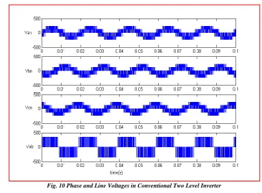
The simulation results carried out using Matlab/Simulink tool box for conventional two-level inverter using space vector modulation scheme is presented.
The data used for simulation is,
Vsa = 230
0
; Vsb = 230
-120
; Vsc = 230
120
; Vab= 350 VFig. 10 Phase and Line Voltages in Conventional Two Level Inverter
Fig.11 Compensation of Sag by DVR for Phase b and c.
VII.
CONCLUSION
2. M. F. Faisal, “Power Quality Management Program: TNB‟s Experience,” Distribution Engineering Department,
TNB, 2005.
3. A. Felce, G. Matas, Y. D. Silva, “Voltage Sag Analysis and Solution for an Industrial Plant with Embedded Induction Motors” Inelectra S.A.C.A. Caracas, Venezuela, 2004.
4. Pirjo Heine, Matti Lehtonen, “Voltage Sag Distributions Caused by Power System Faults” IEEE Transactions on
Power Systems, Vol. 18, No. 4, November 2003.
5. Shairul Wizmar Wahab and Alias Mohd Yusof, “Voltage Sag and Mitigation Using Dynamic Voltage Restorer
(DVR) System” Elektrika Vol. 8, No. 2, 2006, PP 32-37.
6. Rosli Omar, Nasrudin ABD Rahim, Marizan Suleman “Modeling and Simulation for Voltage Sags /Swells Metigation using DVR” Journal of Theoretical and Applied Information Technology © 2005 - 2009 JATIT, PP 464-470
7. H. P. Tiwari and Sunilkumar Gupta, “Dynamic voltage Restorer Based on load condition” International Journal of Innovation, Management and Technology. Vol.1, No.1 April-2010
8. A. Ghosh and G. Ledwich, “Power Quality Enhancement Using Custom Power Devices” Kluwer Academic Publishers, 2002.
9. P. T. Nguyen and T. K. Saha “DVR against Balanced and Unbalanced Voltage Sags: Modeling and Simulation,” IEEE-School of Information Technology and Electrical Engineering, University of Queesland, Australia, 2004.
10. P. S. Bimbhra “Generalized Theory of Electrical Machines” Third Edition Khanna Publishers Delhi.
11. Pirjo Heine, Matti Lehtonen, “Voltage Sag Distributions Caused by Power System Faults,” IEEE Transactions on Power Systems, Vol. 18, No. 4, November 2003.
12. Chris Fitzer, Mike Barnes, and Peter Green, “Voltage Sag Detection for a Dynamic Voltage Restorer” IEEE Transactions on Industry Applications, Vol. 40, No.1, February 2004.
13. P. Boonchiam, N. Mithulananthan, “Understanding of Dynamic Voltage Restorers through MATLAB Simulation,”
Thammasat Int. J. Sc. Tech., 11(3), 2006, PP 1-6.
14. Omar, R., Rahim, N., and Sulaiman, M., “Modeling and Simulation for Voltage Sags/Swells Mitigation Using
Dynamic Voltage Restorer”, Journal of Theoretical and Applied Information Technology, 2009, PP 464-470.
15. S. Deepa and Dr. S. Rajapandian “Voltage Sag Mitigation Using Dynamic Voltage Restorer System” International Journal of Computer and Electrical Engineering, Vol. 2, No. 5, October, 2010, PP 1793-8163
16. H. P. Tiwari and Sunil Kumar Gupta, “Dynamic Voltage Restorer against Voltage Sag” International Journal of Innovation, Management and Technology, Vol. 1, No. 3, August 2010