357 |
P a g e
POWER REDUCTION IN CONTENT ADDRESSABLE
MEMORY
Latha A
1, Saranya G
2, Marutharaj T
31, 2
PG Scholar, Department of VLSI Design,
3Assistant Professor
Theni Kammavar Sangam College Of Technology, Theni, Tamilnadu, (India)
ABSTRACT
Content Addressable Memory (CAM) is a special type of memory which is very helpful in search engines and are much faster. CAM structure composed of conventional semiconductor memory SRAM with some additional circuitry for compare operation. CAM does the operation of returning the address location for a search word in a single clock cycle. CAM performs three types of operations namely READ, WRITE and COMPARE operation. CAM rarely does the READ and WRITE operation and in major scenarios CAM is used for comparing the Search word with the existing database and returning the corresponding address location within a single clock cycle. CAM compares the data word in parallel for each bit and hence consumes higher power. In order to reduce power, the conventional CAM is modified to perform with extra additional count bit as an index bit for each data word. In that way, the time and power consumption can be reduced. In this project, a parity bit based comparison is proposed in contradiction to existing count bit comparison to reduce power. This reduces power to a promising manner.
Keywords: CAM, Associative Memories, Low Power, Parity Bit, Low Power ML, Memory Lookup
Table
I.
INTRODUCTION
Modern digital systems require the capability of storing and retrieving large amounts of information at high speeds.
Memories are circuits or systems that store digitalinformation in large quantity. Semiconductor memory is an
electronic data storage device which often used as computer memory implemented on a semiconductor based
integrated circuits. Semiconductor memory has the property of random access, which means that it takes the same
amount of time to access any memory location, so data can be efficiently accessed in any random order. A memory,
which in one word time finds a matching segment and reads the remainder of the word, has been called by one of
these names as Content-Addressed Memory (CAM) Data Addressed Memory (DAM), Content Associative Memory
(CAM).
II.
MEMORY ORGANIZATION
One of the most important fundamental features of any computing system is the ability to store data to memory,
recall the data, and overwrite the data. In a semiconductor memory chip, each bit of binary data is stored in a tiny
358 |
P a g e
arrays on the surface of the chip. The 1-bit memory cells are grouped in small units called “words” which areaccessed together as a single memory address. Memory is manufactured in word length that is usually a power of
two, typically N=1, 2, 4 or 8 bits. Data is accessed by means of a binary number called a memory address applied to
the chip's address pins, which specifies which word in the chip is to be accessed. If the memory address consists of
M bits, the number of addresses on the chip is 2M, each containing an N bit word. Consequently, the amount of data
stored in each chip is N2M bits. The data capacity is usually a power of two: 2, 4, 8, 16, 32, 64, 128, 256 and 512
and measured in KB-bits, MB-bits, GB-bits or TB-bits, etc. Currently the largest semiconductor memory chips hold
a few GB of data, but higher capacity memory is constantly being developed.
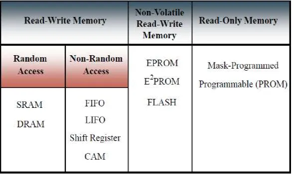
Semiconductor memories are broadly classified into three categories which are shown in below table.
Table 2.1 Memory Classification
Read Write Memories are classified into two categories as
1. Random Access Memories
2. Non – Random Access Memories.
Random-access memory (RAM) is a generic term that refers to both SRAM and DRAM or, indeed, any type of
memory where you can arbitrarily (randomly) access stored data. Non- Random Access Memories are also termed
as “Serial Access Memories”. These are type of memory in which data is accessed sequentially and the time for
access depends on the location of the data desired. In a multiport memory, this term refers to that portion of the
device that is related to the serial-access port and its associated functions.
Content Addressable Memory is one such Serial Access Memories which access the data in a sequence and the
storage device moves through all information up to the point it is attempting to read or write. These are type of
memory which is used for Permanent storage unlike the Random access memories which are used as the temporary
359 |
P a g e
III.
CONTENT ADDRESSABLE MEMORY
Content Addressable Memories (CAMs) are hardware search engines that are much faster than algorithmic
approaches for search intensive applications. CAMs are composed of conventional Semiconductor memory
especially SRAM with added comparison circuitry that enable a search operation to complete in a single clock cycle.
CAM operates in three modes
READ
WRITE
COMPARE
3.1
CAM Architecture
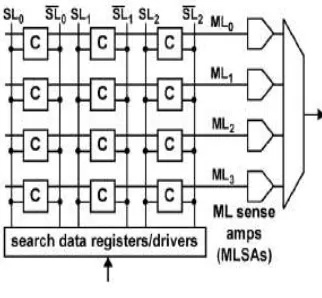
A small model is shown in below figure shows CAM consisting of 4 words, with each word containing 3 bits
arranged horizontally (corresponding to 3 C cells). There is a match -line corresponding to each word (ML0, ML1,
etc.) feeding into match line sense amplifiers (MLSAs), and there is a differential search line pair corresponding to
each bit of the search word (SL0, SL0̅, SL1, SL1̅, etc.). CAM search operation begins with loading the search-data
word into the search-data registers followed by pre-charging all match lines high, putting them all temporarily in the
match state. Next, the search line drivers broadcast the search word onto the differential search lines, and each CAM
core cell compares its stored bit against the bit on its corresponding search lines. Match lines on which all bits match
remain in the pre-charged-high state. Match lines that have at least one bit that misses, discharge to ground. The
MLSA then detects whether its match line has a matching condition or miss condition. Finally, the encoder maps the
match line of the matching location to its encoded address.
Fig 3.1 CAM Architecture
Fig 3.2 10T - NOR based CAM CORE CELL
3.2
Challenges in CAM Design
Full parallel search operation leads to critical challenges in designing a low-power system for speed
360 |
P a g e
Power hungry nature due to the high switching activity of SL and the ML.
A huge surge-on current (i.e., peak current) occurs at the beginning of the search operation due to the
concurrent evaluation of the ML may cause a serious IR drop on the power grid, thus affecting the
operational reliability of the chip.
As a result, numerous efforts have been put forth to reduce both the peak and the total dynamic power consumption
of the CAMs.
3.3
Advantages of CAM
Major advantage that CAM offers are high speed functionality. Other advantages are
Data Storage and retrieval capabilities.
Programming simplification based upon the possibility of ignoring the placement of data in memory and
extensive use of content addressing and ordered retrieval.
Periodicity of structure lends itself to integrated circuit techniques and batch fabrication. Inter connections
between components become shorter and less tangled, reducing propagation delays and simplifying layout
and checkout. Since the structure is periodic, it can be easily expanded in size
The periodic structure may permit an organization which is tolerant of memory or circuit element failures. If
a cell fails, it may be possible to avoid its further use with little loss to the system capability.
3.4
Count Bit Based CAM
In general, a CAM has three operation modes: READ, WRITE, and COMPARE, among which “COMPARE” is the
main operation as CAM rarely reads or writes. It starts a compare operation by loading an n-bit input search word into
the search data register. The search data are then broadcast into the memory banks through n pairs of complementary
search-lines SL and ~SLs directly compared with every bit of the stored words using comparison circuits. Each stored
word has a ML that is shared between its bits to convey the comparison result. Location of the matched word will be
identified by an output encoder, as shown in Figure 1. During a pre-charge stage, the MLs are held at ground voltage
level while both SL and ~SLs are at VDD. During evaluation stage, complementary search data is broadcast to the SL
and ~SL. When mismatch occurs in any CAM cell (for example at the first cell of the row D= “1”; ~D=“0”; SL =“1”;
~SL=“0”), transistor P3 and P4 will be turned on, charging up the ML to a higher voltage level. A sense amplifier
(MLSA) is used to detect the voltage change on the ML and amplifies it to a full CMOS voltage output. If mismatch
happens to none of the cells on a row, no charge up path will be formed and the voltage on the ML will remain
unchanged, indicating a match.
Since all available words in the CAMs are compared in parallel, result can be obtained in a single clock cycle. Hence,
CAMs are faster than other hardware- and software-based search systems. They are therefore preferred in
high-throughput applications such as network routers and data compressors. However, the full parallel search operation
leads to critical challenges in designing a low-power system for high-speed high-capacity CAMs. The power hungry
nature due to the high switching activity of the ML and the SL and a huge surge-on current (i.e., peak current) occurs
361 |
P a g e
power grid, thus affecting the operational reliability of the chip. As a result, numerous efforts have been put forth toreduce both the peak and the total dynamic power consumption of the CAMs.
3.4.1
Pre Computation Scheme Design
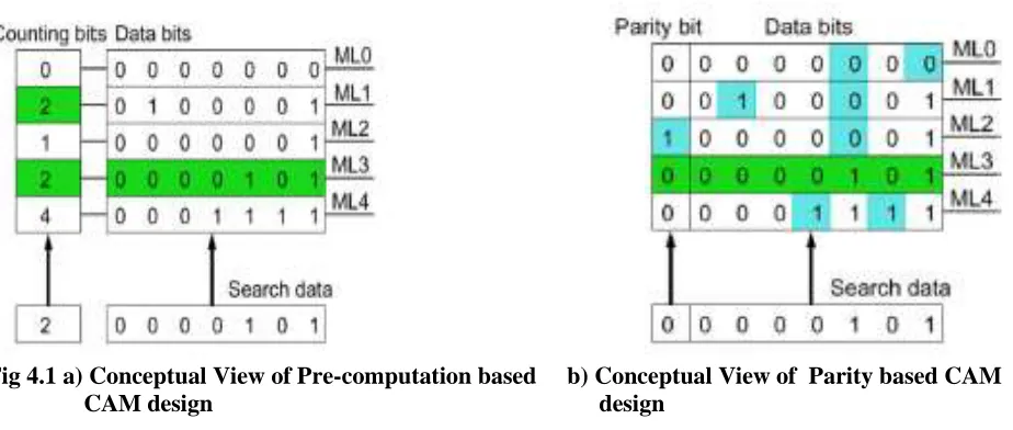
The pre-computation CAM uses additional bits to filter some mismatched CAM words before the actual comparison.
These extra bits are derived from the data bits and are used as the first comparison stage. For example, in below figure
number of “1” in the stored words are counted and kept in the Counting bits segment. When a search operation starts, number of “1”s in the search word is counted and stored to the segment on the left of figure. These extra information are compared first and only those that have the same number of “1”s (e.g., the second and the fourth) are turned on in
the second sensing stage for further comparison. This scheme reduces a significant amount of power required for data
comparison, statistically. The main design idea is to use additional silicon area and search delay to reduce energy
consumption. The previously mentioned pre-computation and all other existing designs shares one similar property.
The ML sense amplifier essentially has to distinguish between the matched ML and the 1-mismatch ML. This makes
CAM designs sooner or later face challenges since the driving strength of the single turned-on path is getting weaker
after each process generation while the leakage is getting stronger. This problem is usually referred to as Ion/Ioff.
IV.
PROPOSED METHOD
A versatile auxiliary bit is introduced to boost the search speed of the CAM at the cost of less than 1% area overhead
and power consumption. This newly introduced auxiliary bit at a glance is similar to the existing Pre-computation
schemes but in fact has a different operating principle.
Fig 4.1 a) Conceptual View of Pre-computation based b) Conceptual View of Parity based CAM
CAM design design
The parity bit based CAM design is shown in above figure consisting of the original data segment and an extra
one-bit segment, derived from the actual data one-bits. Technique is to obtain only the parity one-bit, i.e., odd or even number of
362 |
P a g e
same interface as the conventional CAM with one extra bit. During the search operation, there is only one single stageas in conventional CAM. Hence, the use of this parity bits does not improve the power performance. However, this
additional parity bit, in theory, reduces the sensing delay and boosts the driving strength of the 1-mismatch case
(which is the worst case) by half, as discussed below.
In the case of a matched in the data segment (e.g., ML3), the parity bits of the search and the stored word is the same,
thus the overall word returns a match. When 1 mismatch occurs in the data segment (e.g.,ML2), numbers of “1”s in
the stored and search word must be different by 1. As a result, the corresponding parity bits are different. Therefore
now we have two mismatches (one from the parity bit and one from the data bits). If there are two mismatches in the
data segment (e.g., ML0, ML1 or ML4), the parity bits are the same and overall it has two mismatches. With more
mismatches, we can ignore these cases as they are not crucial cases. The sense amplifier now only have to identify
between the 2-mismatch cases and the matched cases. Since the driving capability of the 2-mismatch word is twice as
strong as that of the 1-mismatch word, the proposed designgreatly improves the search speed and the Ion/Ioffratio of the
design
.
Table 4.1 Memory Lookup Table for Parity based design
Parity Bit
Data
0
1111
1
0010
0
0011
0
0000
0
0101
0
0110
1
0111
1
1000
0
1001
0
1010
1
1011
0
1110
V.
SIMULATED RESULTS
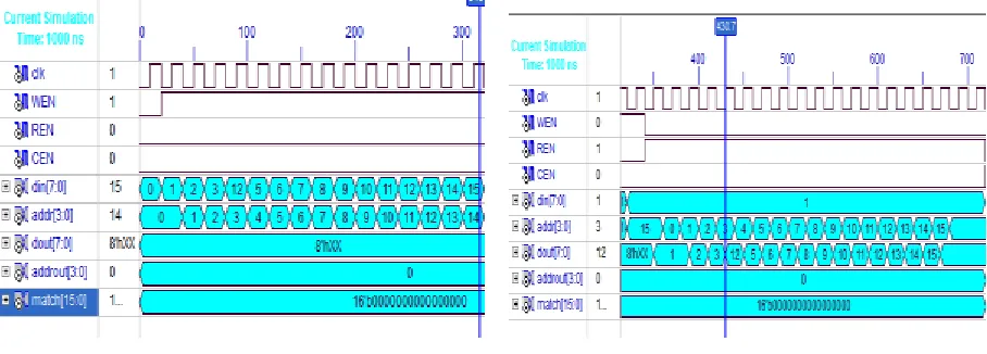
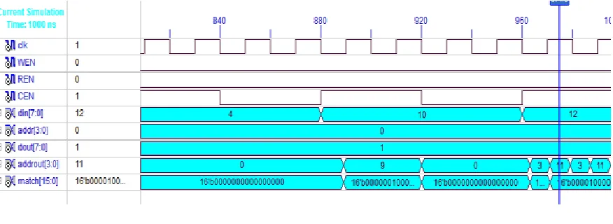
The Memory circuits are developed through Verilog HDL using XILINX ISE Simulator (Version 9.2i). Read, Write
and Compare operations for both the techniques are simulated along with their power analysis. Power analysis is
363 |
P a g e
Fig. 5.1 Write Operation of CAM Fig 5.2 Read Operation of CAM
Table 5.1 Memory Look-up Table
Count Bit
Address
Data
1
0000
0001
1
0001
0010
2
0010
0011
1
0011
0100
2
0100
0101
2
0101
0110
3
0110
0111
1
0111
1000
2
1000
1001
2
1001
1010
3
1010
1011
364 |
P a g e
Fig 5.3 Compare Operation of CAM
CAM circuits are developed for both read, write and compare operation for both pre computation based and parity
based design techniques. From Results we analyzed that Parity based CAM circuits consume less power when
compared to the count bit based pre computation CAM. Also the search speed is also better in the parity based CAM
design.From the above power comparison table, it is clear that Content Addressable Memory logic implemented
based on Parity bit logic consumes lesser power when compared to the Content Addressable Memory logic
implemented with the conventional pre-computation based design of logic implementation using Count bit method.
Table 5.2Power Consumption in Count and parity based technique
.
Power Analysis
RESULTS
COUNT
BASED
CAM
PARITY
BASED
CAM
Total Power
Consumption
95mw
91mw
VI.
CONCLUSION
Reliability of a product describes the ability of a system or component to perform its required functions under stated
conditions for a specified period of time. Quality of product is decided based on reliability of the chip. For an
Integrated Circuit (IC), as a critical product specification under today’s aggressive technology scaling, reliability has
always been very difficult and costly to measure, and to achieve in leading-edge technology. In this paper, a novel
low-power and highly reliable Content Addressable Memory logic has been proposed to increase the search speed
and reduce the power consumption during compare operation. Thus two various techniques are developed to identify
365 |
P a g e
measures are taken to reduce the power in compare cycle. Basically the existing conventional CAM follows theapproach of pre-computation method of adding an extra count bit which stores the number of count based
comparison and hence the new technique proposed is based on the parity bit based comparison which helps in power
reduction. Both these techniques are developed and simulated to analyze the power consumption and simulated
results shows that Parity based CAM boost the search speed with reduced power consumption.
REFERENCES
1. Arsovski, I. and Sheikholeslami,A. “A mismatch-dependent power allocation technique for match-line
sensing in content-addressable memories,” IEEE J. Solid-State Circuits, vol. 38, no. 11, pp. 1958–1966, Nov.
2003.
2. Baeg, S. “Lowpower ternary content-addressable memory design using a segmented match line,” IEEE
Trans. Circuits Syst. I, Reg. Papers, vol. 55, no. 6, pp. 1485–1494, Jul. 2008.
3. Do,A. T. Chen, S. S. Kong,Z. H. and Yeo,K. S. “A low-power CAM with efficient power and delay
trade-off,” in Proc. IEEE Int. Symp. Circuits Syst. (ISCAS), 2011, pp. 2573–2576.
4. Do, A. T. Chen, S. S. Kong, Z. H. and Yeo, K. S.” A High Speed Low Power CAM With a Parity Bit
andPower-Gated ML Sensing,” IEEE Trans. Very Large Scale Integr. (VLSI) Syst., vol. 21, no. 1, Jan.2013.
5. Mohan, N. Fung, W. Wright,D. andSachdev,M. “A low-power ternary CAM with positive-feedback
match-line sense amplifiers,” IEEE Trans. Circuits Syst. I, Reg. Papers, vol. 56, no. 3, pp. 566–573, Mar. 2009.
6. Mohan, N. and Sachdev,M. “Low-leakage storage cells for ternary content addressable memories,” IEEE
Trans. Very Large Scale Integr. (VLSI) Syst., vol. 17, no. 5, pp. 604–612, May 2009.
7. Pagiamtzis, K. and Sheikholeslami, A. “A low-power content-addressable memory (CAM) using pipelined
hierarchical search scheme,” IEEE J. Solid-State Circuits, vol. 39, no. 9, pp. 1512–1519, Sep. 2004.
8. Pagiamtzis, K. and Sheikholeslami, A. “Content-addressable memory (CAM) circuits and architectures:A
tutorial and survey,” IEEE J. Solid State Circuits, vol. 41, no. 3, pp. 712–727, Mar. 2006.
9. Tyshchenko, O., and Sheikholeslami,A. “Match sensing using matchline stability in content addressable
memorys (CAM),” IEEE J. Solid State Circuits, vol. 43, no. 9, pp. 1972–1981, Sep. 2008.
BIOGRAPHICAL NOTES
MS.LATHA A is presently pursuing M.E final year in Electronics and Communication Engineering Department (specialization in VLSI design) from TheniKammavarSangam College of Technology, Theni, Tamilnadu, India. She
completed her Bachelor of Engineering in ECE from Anna University, Tamilnadu in the year 2006.
MS.SARANYA G is presently pursuing M.E final year in Electronics and Communication Engineering Department
(specialization in VLSI design) from TheniKammavarSangam College of Technology, Theni, Tamilnadu, India. She
366 |
P a g e
MR.T.MARUTHARAJ, M.E. is working as an Assistant Professor in Electronics and Communication Engineering Department, from TheniKammavarSangam College of Technology, Theni, Tamilnadu, India. He completed his M.E