*Corresponding author: [email protected]
1
Indoor Optical Wireless Receiver – Theory And Design
M.F.L. Abdullah
1,*, R.J Green
21Faculty of Electrical & Electronic Engineering, University Tun Hussein Onn Malaysia 2School of Engineering, University of Warwick, United Kingdom
Received 1 March 2011; accepted 30 October 2011, available online 24 December 2011
1.
Introduction
The purpose of this paper is to provide insight into the research effort to date in optical wireless receiver both in academic and industrial contexts. The idea of using the optical medium for wireless communications is not new, having been proposed as a means for indoor communications almost two decades ago.[4][6][7] However, recent years have seen an increasing interest in the potential for free space optical systems to provide portable data communications. One of the main aspects for reconsidering the use of an optical carrier in the wireless context is the demand for greater transmission bandwidths. The radio frequency spectrum is already exceedingly congested and frequency allocations of sufficient bandwidths are extremely hard to obtain. Proponents of optical wireless systems argue that the optical medium is the only cost-effective way to provide high bit-rate mobile services to volume markets. In most proposed infrared optical wireless communication [4-10], it is well known that the signal level in an optical wireless receiver is weakest at the front end. Weakest front end means that it is too noisy, too slow or both. The two parameters are not unrelated; it is easy to have a fast front end by preparing to sacrifice signal to noise ratio. This is where the system signal-to-noise ratio is determined and system performance level established.
2.
Photodetector Input-Output
Relationships
Semiconductor junctions that convert photon energy of light into an electrical signal by releasing and accelerating current-conducting carriers, ultimately to produce a baseband voltage for regeneration is called a photodiode.[1] In order to appreciate its performance in practical optical wireless systems, we have to characterize the photodiode from three points of view : the physical viewpoint, the circuit viewpoint and the statistical viewpoint.
The physical viewpoint
The presence of incident optical power, entering a semiconductor device produces thermal agitation that release holes-electron pairs generated at various points within the diode as illustrated in Fig 1.[2] These carriers drift toward opposite ends of the device under the influence of the applied field. When a carrier passes through the high-field region, it may gain sufficient energy to generate one or more new pairs of holes and electrons through collision ionization. These new pairs will in turn generate additional pairs by the same mechanism. Carriers accumulate at opposite ends of the diode, thereby reducing the potential across the device until they are removed by the biasing and other circuitry in parallel with the diode as shown in Fig 2. The chances that a carrier will generate a new pair when passing through the high-field region depends upon the type of
Abstract: This paper presents a systematic approach to the design of receiver for indoor optical wireless communication. In particular, it is concerned with how one can properly chooses the front-end preamplifier and biasing circuitry for the photodetector. A comparison between differences types of amplifier, and bandwidth enhancement technique is also discussed. For most photodetector applications, large values of RL and CD would severely restrict bandwidth. It is shown that a proper front-end design incorporates a transimpedance preamplifier which tends to integrate the detector output. Such a design provides significant reduction in photodiode capacitance and increase bandwidth when compared to a design which does not integrate initially. Two novel techniques, using bandwidth adjustment for better service quality with a bootstrapped transimpedance amplifier and bootstrapped composite transimpedance amplifier is presented. A controllable capacitance is introduced at the output of the second stage of the amplifier. These technique permits a bandwidth adjustment from 52Hz to 233MHz for a capacitance range of 10uF to 1pF, while the composite amplifier bandwidth adjustment of the circuit can be controlled in the frequency range of 6MHz to 60MHz for a capacitance range of 50pF to 1nF.
Keywords:photodetector, boostrap transimpedance preamplifier, composite transimpedance amplifier
*Corresponding author: [email protected]
1
Indoor Optical Wireless Receiver – Theory And Design
M.F.L. Abdullah
1,*, R.J Green
21Faculty of Electrical & Electronic Engineering, University Tun Hussein Onn Malaysia 2School of Engineering, University of Warwick, United Kingdom
Received 1 March 2011; accepted 30 October 2011, available online 24 December 2011
1.
Introduction
The purpose of this paper is to provide insight into the research effort to date in optical wireless receiver both in academic and industrial contexts. The idea of using the optical medium for wireless communications is not new, having been proposed as a means for indoor communications almost two decades ago.[4][6][7] However, recent years have seen an increasing interest in the potential for free space optical systems to provide portable data communications. One of the main aspects for reconsidering the use of an optical carrier in the wireless context is the demand for greater transmission bandwidths. The radio frequency spectrum is already exceedingly congested and frequency allocations of sufficient bandwidths are extremely hard to obtain. Proponents of optical wireless systems argue that the optical medium is the only cost-effective way to provide high bit-rate mobile services to volume markets. In most proposed infrared optical wireless communication [4-10], it is well known that the signal level in an optical wireless receiver is weakest at the front end. Weakest front end means that it is too noisy, too slow or both. The two parameters are not unrelated; it is easy to have a fast front end by preparing to sacrifice signal to noise ratio. This is where the system signal-to-noise ratio is determined and system performance level established.
2.
Photodetector Input-Output
Relationships
Semiconductor junctions that convert photon energy of light into an electrical signal by releasing and accelerating current-conducting carriers, ultimately to produce a baseband voltage for regeneration is called a photodiode.[1] In order to appreciate its performance in practical optical wireless systems, we have to characterize the photodiode from three points of view : the physical viewpoint, the circuit viewpoint and the statistical viewpoint.
The physical viewpoint
The presence of incident optical power, entering a semiconductor device produces thermal agitation that release holes-electron pairs generated at various points within the diode as illustrated in Fig 1.[2] These carriers drift toward opposite ends of the device under the influence of the applied field. When a carrier passes through the high-field region, it may gain sufficient energy to generate one or more new pairs of holes and electrons through collision ionization. These new pairs will in turn generate additional pairs by the same mechanism. Carriers accumulate at opposite ends of the diode, thereby reducing the potential across the device until they are removed by the biasing and other circuitry in parallel with the diode as shown in Fig 2. The chances that a carrier will generate a new pair when passing through the high-field region depends upon the type of
Abstract: This paper presents a systematic approach to the design of receiver for indoor optical wireless communication. In particular, it is concerned with how one can properly chooses the front-end preamplifier and biasing circuitry for the photodetector. A comparison between differences types of amplifier, and bandwidth enhancement technique is also discussed. For most photodetector applications, large values of RL and CD would severely restrict bandwidth. It is shown that a proper front-end design incorporates a transimpedance preamplifier which tends to integrate the detector output. Such a design provides significant reduction in photodiode capacitance and increase bandwidth when compared to a design which does not integrate initially. Two novel techniques, using bandwidth adjustment for better service quality with a bootstrapped transimpedance amplifier and bootstrapped composite transimpedance amplifier is presented. A controllable capacitance is introduced at the output of the second stage of the amplifier. These technique permits a bandwidth adjustment from 52Hz to 233MHz for a capacitance range of 10uF to 1pF, while the composite amplifier bandwidth adjustment of the circuit can be controlled in the frequency range of 6MHz to 60MHz for a capacitance range of 50pF to 1nF.
carrier, the material out of which the diode is constructed and the voltage across the device. The depth and extent of the junction determines the location of the depletion region and the light wavelengths that produce an efficient response. For a given photodiode and a given wavelength, a photodiode responsivity expresses the resulting efficiency through[2]
Ip = rØØe
where rØ – diode’s flux responsivity and Øe – radiant flux energy in watts
Fig. 1 Photodetector
The circuit viewpoint
From the discussion above and more detailed investigation, modeling the characteristics of the photodiode with discreet circuit components permits analysis of application circuits. Fig 2 shows the resulting model with an ideal diode, a current source and parasitic elements. Cd is the junction capacitance of the diode across which voltage accumulates when charges produced within the device separate under the influence of the bias field. The current generator ip(t) represents the production of charges by optical and thermal generation and collision ionization in the diode high-field region. Resistance RD represents the diode’s dark resistance, which is the resistance of the zero-biased diode junction. In order to use the photodiode efficiently we must design a circuit which will respond to the current ip(t) with as little distortion and added noise as possible. In order to derive information from the circuit responding to ip(t) we must understand the statistical relationship between ip(t) (the equivalent current generator) and the incident optical power p(t).[1-2]
The statistical viewpoint
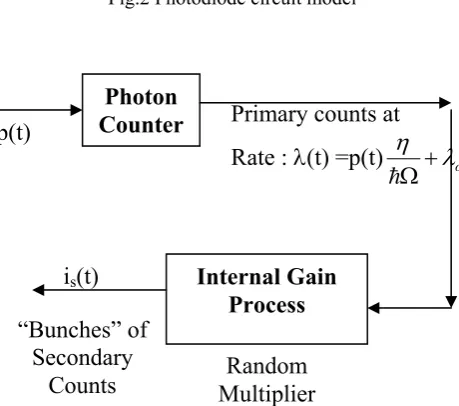
In Fig 2, the current source ip(t) can be considered to be a sequence of impulses corresponding to electrons generated within the photodiode due to optical or thermal excitation or collision ionization. From various physical studies it has been concluded that for cases of current interest, the electron production process can be modeled as shown in Fig 3. Let the optical power falling upon the photon counter be p(t). In response to this power and due to thermal effects, the photon counter of Fig 3 produces electrons at average rate λ(t) per second where
λ(t) = [(η/hΩ)p(t)] + λo (1)
where η – photon counter quantum efficiency hΩ – energy pf a photon
λo – dark current “counts” per second
λ(t) is only the average rate at which electrons are produced. p(t) the number of electronic produced in any interval is statistically independent of the number produced in any other disjoint interval.[1]
Fig.2 Photodiode circuit model
Fig.3 Model of is(t) generationprocess
Each of the primary impulses produced by the photon counter enters a random multiplier where, corresponding to collision ionization it is replaced by g contiguous “secondary” impulses. The number g is governed by the statistics of the internal gain mechanism of the photodiode. Each primary impulse is “multiplied” in this manner by a value g which is statistically independent of the value g assigned to other primaries. Thus the current leaving the photodiode consists of bunches of electrons. For applications interest here, it will be assumed that all electrons in a bunch exit the photodiode at the time when the primary is produced. This shows that the duration of the photodiode response to a single primary hole-electron pair is very short compared to the response times of circuitry to be used with the photodiode.
Photodiode Variations
“Bunches” of
Secondary
Counts
Multiplier
Random
Primary counts at
Rate :
(t) =p(t)
o
p(t)
is(t)
Internal Gain
Process
Photon
Two variations of the basic photodiode improve the diode’s response. Physical study shows that PIN photodiodes increase the spectral bandwidth or range of light frequencies that produce an efficient photo response. Avalanche photodiodes increase the magnitude of the output current and the response speed by permitting diode bias at the verge of breakdown. For application interest, PIN photodiode is preferably in optical wireless communication system.
Noise Contributions : As a photodiode amplifier, the current to voltage converter exhibits a complex noise behavior. The major sources of noise in front ends are listed in Table 1, where eN and iN are rms values of random fluctuations.[6],[9]
Table 1 Noise source
Source Type Formula Dominates When :
Photocurrent Shot
noise i(2eINSHOTd)1/2 =
Bright light, large load
resistor Load resistor Johnson
noise (4kT/R)INth = 1/2 Dim light, small R
Amplifier Input
current noise
iN =
R
kT
4
Ideally, never
Input voltage
noise
eN =
kTR
4
Dim light, large RC or a fast noisy amp
3.
Theoretical Insight of Transimpedance
Amplifier
This section of the paper explained an example of how to design a front-end amplifier for a visible or near IR photodiode and how to get improvement in bandwidth without a big sacrifice of SNR.
Given a detector (Fig 2) whose output is a current, the easiest way to form a voltage from it is to have a load resistor (RL). The output full swing appears across the detector capacitance Cd, rolls off starting at fRC =
D L
C
R
2
1
. The signal voltage Vo(f) =
f
C
R
j
R
f
i
D L
L p
2
1
)
(
. Reducing RL will reduce the RCproduct and speed up the system, while increasing RL increase the bandwidth and dynamic range of the system. Another key idea is to reduce the swing across CD, by making the detector work into a virtual ground using a transimpedance amplifier shown in Fig 4.[6],[9] The inverting input of A1 draws no current, feedback forces the voltage there to be close to zero at all times. A1 senses the voltage across CD and wiggles other end of RF to zero
it out. Provided that A1 has high loop gain AVOL, the swing across CD is greatly reduced and the bandwidth greatly improved. The amplifier input adds a significant amount of its own capacitance Cin. For a typical transimpedance topology using active devices with load feedback resistance Rf , the transimpedance gain Az can be approximated by :
Az
VO in D f
f
A
C
C
R
j
R
)
(
1
(2)
where Avo is the open loop voltage gain of the amplifier and is the angular frequency.
The transimpedance rolls off depends on the magnitude of the impedance of the feedback elements. Therefore the transimpedance amplifier bandwidth is calculated with the following equation :[6],[9]
f3dB
2
T RCf
f
(3)where fT is the unity-gain crossover frequency
Equation 2 shows that the upper 3dB cut-off frequency of the preamplifier is a function of the capacitance from the detector, feedback resistor and open loop voltage gain. In other words, a large detector means a large Cd. Hence, in order to achieve large bandwidths either the value of Rf is reduced or Avo is increased. Unfortunately, increasing Avo will jeopardize amplifier stability and reducing Rf will increase thermal noise into the system.
Fig. 4 Transimpedance amplifier circuit and noise model
currents add linearly, the other end of iNth is at ground for noise purpose. The rolloff in the frequency response does not degrade the signal to current noise ratio. The amplifier’s voltage noise, eNamp is treated differently because A1 is a differential amplifier. Therefore eNamp is multiplied by A1’s noninverting gain.[6],[9]
AVcl =
f D Vol Vol
R
jwC
A
A
1
1
(4)
If eNamp is very low or if we are not trying to get a huge bandwidth improvement through (fT*fRC)1/2 mechanism, this rising noise contributions will not limit. Otherwise, it will dominate the noise starting at :
f3dB =
L Namp D D
Namp
R
kT
i
eI
C
e
4
2
2
1
2
(5)In order that op amp do not dominate the noise according to Hobbs[9], we should choose it by the following rules :
iNamp < 0.5iNth (Noise of Rf dominates iNamp)
eNamp < 0.5 Rf iNth (eNamp should be the same in flatband) eNamp < 0.5iNth / (2πf3dB (CD + Cin) (Noise peak should not dominate anywhere in the frequency band)
fT > 2f3dB2/ fRC (The amplifier has to raise enough bandwidth)
fT < 10f3dB2 / fRC (Speed too fast risks trouble with ringing and oscillation)
The transimpedance amplifier does not improve the SNR of the photodiode it just changes the frequency response. There’s nothing inherent or inescapable about noise peak in system, it comes from a poor choice of circuit topology that can be amended.
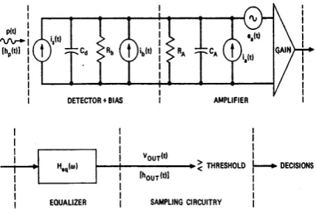
Fig. 5 High impedance amplifier with equalizer
High impedance amplifier theory : Fig 5 shows a typical receiver in schematic form consisting of a photodiode, an amplifier and an equalizer. This amplifier is modeled as an ideal high-gain impedance amplifier with an equivalent shunt capacitance and resistance at the input, in addition with two noise sources referred to the input.
The noise sources for this particular part will be assumed to be white, Gaussian and uncorrelated. It is also assumed that amplifier gain is sufficiently high, that the noises introduced by the equalizer are negligible.
The average detector output current, iS(t) is given by :[1] iS(t) =
ep
t
e
o
)
(
(6)
where e = electron charge, λo = dark current electrons/second,
)
(
t
p
= average optical primary electrons/second.
Therefore the average voltage (neglecting dc components) at equalizer output, where “ * “ indicates convolution and A is an arbitrary constant :
vout(t) =
A
ep
(
t
)
*
h
fe(
t
)
*
h
eq(
t
)
(7)
hfe(t) = F{
)
(
1
1
A d T
C
C
j
R
} is the amplifier input
circuit current impulse response RT =
[
1
1
]
1A b
R
R
isthe total detector parallel load resistance heq(t) is the equalizer impulse response
High impedance amplifier tends to give a degraded frequency response as the bandwidth relationship
B
C
C
R
b d A
)
(
2
1
is not maintained for widebandoperation[1]. The detector output is effectively integrated over a large time constant and must be restored by differentiation. This is performed with the correct equalization. Therefore the high impedance front end gives a better improvement in sensitivity over the low impedance front end design, but eventually creates a heavy demand for equalization and has problem of limited dynamic range. The limited dynamic range is because of the attenuation from the low frequency signal components by the equalization process which causes the amplifier to saturate at high level signals. If the amplifier is saturated before equalization has occurred the signal will be heavily distorted, thus reducing the dynamic range which is dependent upon the amount of integration and subsequent equalization employed.
4. Bootstrap Transimpedance Amplifier
impedance amplifier with positive or negative feedback. Bandwidth enhancement techniques are required that do not affect low frequency behavior, so that both high dc gain and large bandwidth can be obtained. Several of these techniques have been proposed in the literature in order to maximize the gain-bandwidth product of an amplifier stage.
One of the method is a transimpedance amplifier is built up with two capacitive coupled voltage dividers (R1-R2, R3-R4) instead of a single feedback resistor[10]. The basic concept of this network is its different behavior at low and high frequencies. At low frequencies the transimpedance of the transimpedance amplifier is approximately the sum of R1 and R2. For higher frequencies the parasitic capacitance of resistor R2 has no effect owing to the low resistance of R4, which has no effect on the bandwidth of the transimpedance amplifier. Only parasitic capacitance of resistor R1 has an influence on the bandwidth of the circuit at a nine times higher frequency than before.
Cascading and capacitance neutralization compensate the input Miller capacitance thus expanding the bandwidth if the input pole is dominant. Unfortunately these techniques are less effective in low power amplifiers that use high speed bipolar transistors, if the output pole becomes dominant.
Another well known method to increase bandwidth of amplifiers uses peaking capacitors[8] or inductors. This method usually places inductors or capacitors in a strategic location of the amplifier circuit, resulting in a resonance with parasitic capacitances, which broadens the bandwidth of the amplifier. Although inductive peaking do increase the amplifier bandwidth, stray capacitances of the inductor often causes bandwidth degradation rather than an improvement. Capacitive peaking design is preferable, but this technique is extremely sensitive to process variations and could cause large peaking.
Therefore, a much improved version of a front-end, incorporated within a transimpedance amplifier, is shown in Fig 6, the topology being known as the bootstrapped transimpedance amplifier (BTA)[11]. The BTA is an attractive design as it reduces the effective detector capacitance, Cd, seen by the signal. The output of the emitter follower stage is feedback to the photodetector by a bootstrapping capacitor, C3. Fig 7 proposes a combination of bootstrapped technique with a capacitive peaking technique by placing a capacitor, C4, in series with the emitter resistor in the second gain stage, with a feedback resistor R8 [12]. By varying the capacitor, the bandwidth of the circuit can be controlled. The output results of Fig 6 and Fig 7 are shown in Fig 8 and Fig 9. In each case the amplifier output is taken from the collector at Q3. Assuming that the gain stages and the emitter follower can be approximated by a simplified hybrid-
model, as shown in Figure 10,
R
1,
R
2
R
7 and weconsider frequencies where C1, C2 and C3 are short
circuits, the transimpedance gain, Az for the circuit is approximated by equation (8):
Az =
]
)
1
(
[
]
1
)[
1
(
)]
1
(
2
[
7 7 3 3 4 3
3
7 3 6 3
R
R
g
r
C
j
g
r
A
A
R
r
R
g
I
V
m m
m
p o
(8)
where A is the voltage gain of the first stage amplifier
Fig. 6 Bootstrapped transimpedance amplifier circuit
Fig. 7 Bootstrapped with capacitor peaking transimpedance amplifier circuit
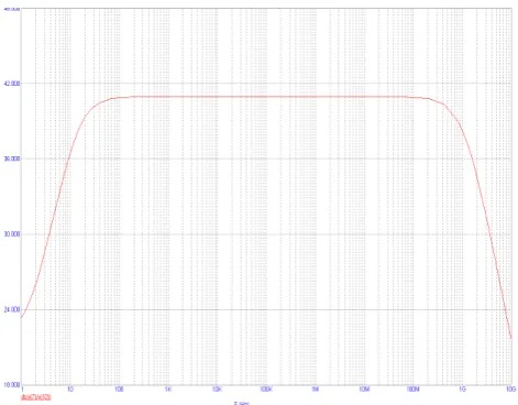
Fig. 8 Frequency response bootstrapped transimpedance amplifier
Fig. 9 Frequency response bootstrapped with capacitor peaking transimpedance amplifier
Fig.10 Model hybrid-pi of bootstrapped with capacitor peaking transimpedance amplifier circuit
A better proposed topology using a composite amplifier provides high bandwidth as shown in Fig 11. The bootstrapped transimpedance amplifier is connected in series with a voltage feedback amplifier and a RC filter. By varying the capacitor, C6 between 50pF to 1nF the bandwidth of the circuit can be controlled in the frequency range of 6MHz to 60MHz as shown in Fig 12. There is a trade-off between gain and bandwidth compared to Fig 9. As the bandwidth is increased the gain of the circuit is reduced. If we assume that the gain stages, the emitter follower and second stage amplifier can be approximated by a simplified hybrid- model, as shown in Figure 13. The transimpedance gain, Az1 for the circuit can be approximated by equation (9) considering frequencies where C1, C2 and C3 are short circuits :
Az1 =
)
1
)(
(
]
[
20 6 1
1 19 1 19 3
3 6 7 7 1 6 1 19 2
R
C
j
R
A
R
R
R
r
r
R
AR
R
A
R
R
R
I
V
i i
i
p o
(9)
where A is the voltage gain of the first stage amplifier and A1 is the voltage gain of the second stage amplifier.
Bootstrapping transimpedance amplifier effectively allows for a higher transimpedance gain and a lower Rf thermal noise contribution. Composite configuration of transimpedance amplifier effectively allows for a higher bandwidth with a trade-off of 10dB – 20dB gain, while maintain its noise contribution.
Fig. 12 Frequency response composite transimpedance amplifier
Fig. 13 Model hybrid-pi of composite transimpedance amplifier
5.
Transimpedance Amplifier ImplementationIn application wise, base on the above simulation design it is suggested that the composite amplifier receiver to be use to accommodate the high frequency range bandwidth adjustment, where a variable switching capacitor circuit could be use to vary the capacitance from the range of 50pF to 1nF. The propose switching circuit which is design to be incorporated together with the receiver will
then automatically select the right capacitance value based on the input received signal quality and adjust the receiver to the required bandwidth.
6.
Summary
Receiver design is particularly challenging because not only dynamic range and bandwidth criteria has to be met, but also significant problems of high ambient light levels noise has to be dealt with. This paper has provided an insight issues associated with the front-end design of a wireless infrared communication. It has highlighted the significant maxims on choosing the biasing circuitry. To summarize, high impedance amplifier with a large Rf diminish the effects of thermal noise. However the receiver bandwidth is then usually smaller then the signal bandwidth, which require an equalization stage following the preamplifier as discussed. The circuit will be tricky, as the equalizer effect reduces the overall dynamic range of the receiver. The transimpedance front ends resolve these issues by using a large feedback resistor and an inverting amplifier, which boots the bandwidth without thermal noise and dynamic range problems. In addition, infrared application dominant source of noise is due to background radiation, not thermal and circuit noise, which makes the sensitivity of the transimpedance front end more attractive. Therefore, in conclusion, infrared optical wireless communication had yet to fully exploit all the potential benefits offered by the medium. There is still a great deal of work to be done in the adaptation and optimization of coverage areas, especially with unknown receiver orientation
A
CKNOWLEDGMENTThe author wish to thank the Malaysian Government for the sponsorship
References
[1] S.D. Personick, “Receiver Design for Digital Fiber Optic Communication Systems I” The Bell System Technical Journal, Vol : 52, (1973), pp : 843 – 874 [2] Graeme, J. G, “Photodiode amplifiers : Op amp solutions”, McGraw Hill (1985)
[3] R.J. Green, M.G. Mcneill, “Bootstrap transimpedance amplifier : a new configuration”, IEE proceedings, Vol :136, No : 2 (1989), pp : 57-61
[4] John R.Barry, “Wireless Infrared Communications” Kluwer Academic Publishers, 1994
[5] A.M.Street, P.N.Stavrinou, D.J.Edwards and G.Parry, “ Optical Preamplifier designs for IR-LAN
Applications” IEE (1996), pp : 8/1-8/6
[6] Stephen B.Alexander, “Optical Communication Receiver Design” IEE Telecommunications Series, Vol 37 and SPIE Tutorial Texts in Optical
[7] A.M.Street, P.N.Stavrinou, D.C.O’Brien and D.J.Edwards, “ Indoor optical wireless systems – a review” Optical and Quantum Electronics 29 (1997), pp : 349-378
[8] Feng-Tso. Chein, Yi-Jen. Chan, “Bandwidth enhancement of transimpedance amplifier by a capacitive-peaking design”, IEEE Journal of Solid- State Circuits, Vol : 34, No : 8 (1999), pp :1167-1170 [9] Philips C.D. Hobbs, “Building Electro-Optical Systems : Making it All Work”, John Wiley & Sons Inc, (2000), pp : 620 – 666
[10] C. Seidl, J.Knorr , H. Zimmermann, “Simple
feedback network for bandwidth enhancement of transimpedance amplifiers”, Electronics Letters, Vol : 39, No : 25 (2003)
[11] Abdullah M.F.L,Green.R, Leeson.M, “Optical wireless communication front-ends” High frequency Postgraduate Student Colloquium 2004, pp : 3-8 [12] Abdullah M.F.L, Green R.J, “Receiver Amplifier Technique For Dynamic Service Quality Adaptation In Optical Wireless Communication” 4th