e-ISSN: 2278-067X, p-ISSN: 2278-800X, www.ijerd.com
Volume 13, Issue 12 (December 2017), PP.31-38
Address Mapping In Content Addressable Memory Interface
with A Low Power Approach
K.Suresh Kumar
1,Y.Rajasree Rao
2, K.Manjunathachari
31Asst.Prof., ECE Dept., SSJEC, Hyderabad, 2Prof &Dean, St.Peter’s Engg College, Hyderabad,.3Prof.&HOD,
ECE Dept., Gitam University, Hyderabad, India.
ABSTRACT:
The addressable memory contents are pointed using address pointer. In the addressing mode, the address pointer is programmed to generate addressing location in a sequence and pass to the data bus. Here, the address pointers are used to fetch the data in a predefined sequence and the variability in address pointer would leads to high power consumption. This variability, leads to high transition and hence leads to transitional power consumption in memory interface. To minimize the power consumption, in this paper, a new reordered memory interface with correlative transition optimization is presented.Keyword:
Address mapping, content addressable memory interface, low power address realignment.
--- Date of Submission: 13 -12-2017 Date of acceptance: 26-12-2017
---I. INTRODUCTION
With the evolution of VLSI design, the major concerns of the VLSI designer were area, performance, cost and reliability; power consideration was mostly of only secondary importance. In recent years, however, this has begun to change and, increasingly, power is being given comparable weight to area and speed considerations. Several factors have contributed to this trend. Perhaps the primary driving factor has been the remarkable success and growth of the class of personal computing devices (portable desktops, audio- and video-based multimedia products) and wireless communications systems (personal digital assistants and personal communicators) which demand high-speed computation and complex functionality with low power consumption. In these applications, average power consumption is a critical design concern. In the memory interfacing, this issues is more effective due to continuous data accessing. To optimize the power consumption in content addressable memory interface (CAM) In [1] algorithm to compile regular expression patterns into combinatorial circuits based on nondeterministic finite automaton is suggested. [2] Developed a module generator that shared common prefixes to reduce the circuit area on FPGA. [3] Presented a content-scanning module on FPGA for an internet firewall. [4] Improved area and throughput by adding pre-decoded wide parallel inputs to traditional NFA implementations. [5] Presented a pre-decoded multiple-pipeline shift-and-compare matcher which reduced routing complexity and comparator size by converting incoming characters into many bit lines. [6] proposed a sharing architecture which significantly reduces circuit areas by sharing common infix and suffix sub-patterns. From the perspectives of reconfigurability and scalability, memory architectures are attractive because memory is flexible and scalable.
II. ADDRESS MAPPING IN CAM
Content addressable memory addressing is an integral part of the memory interfacing operation. In the approach of memory interfacing, address are been generated as a address pointer, to generate addressing location, in the CAM operation, address pointers are decoded from the address decoder unit and allocated to the memory interfacing based on user interfacing. In the operation of address pointing, CAM, examine the contents of the entire memory to derive the pattern. Due to direct accessing mode, this memory has a faster interfacing as compared to RAM. The CAM memory interface is developed as a set of encoder, decoder and mapper logic to derive a mapping operation in CAM application. A basic interfacing unit for CAM data access is illustrated in figure 1.
Figure 1: Interface unit for CAM data access
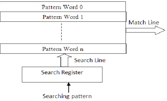
In the process of CAM accessing, data are exchanged in binary or ternary representation called TCAM, where a don‟t care „X‟ is introduced for bit which are of no significance in matching. The ternary representation are hence more faster in access then binary representation. During the search operation, a search data register is initialized which defines a set of test patterns to search over the stored words. The search register are mapped to match register which intern decode to generate the result. The matching operation of this CAM operation is outlined in figure 2.
Figure 2: Operational diagram of a CAM mapping
In the operational stage of CAM accessing, the stored words are matched to the search register data to make a decision. These memory interface are predominantly been used in routers, security checking, firewalls, etc. The operation illustrates a very high interfacing transition in matching and data transfer, which leads to a high level of power dissipation in memory interfacing. It is hence, primarily required to minimize this power consumption for optimal CAM performance.
III. REORDER MEMORY INTERFACING
pattern, no power optimization concern is been focused. It is observed that the power dissipation is high in CAM application. To conserve power dissipation, block register [8] and counter based operation [5] were proposed. Wherein operational approach were focused in power conservation, pattern based power optimization is not focused. The power required for the storage of memory data and accessing depends on the content of this memory. As observed, each of a bit transition result in power dissipation, and the storage power required in memory storage is an additional count. In the memory interfacing, each of the transition has a volume of power dissipation given by,
𝑃𝑑 = 𝐶𝑚𝑉𝐷𝐷2 𝑁𝑡𝑟 𝑙𝑖𝑛𝑒
Here, 𝐶𝑚 is the capacitance attached to the memory unit, VDD is the voltage to the line, and 𝑁𝑡𝑟 are the
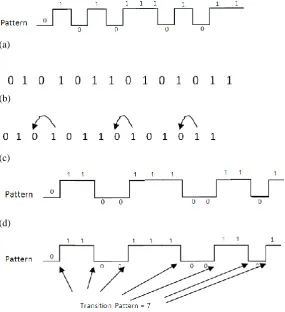
numbers of transition observed. As capacitance of the memory and the VDD to the memory unit remain constant, it is observed that the power dissipation is proportional to the number of transition in a pattern observed. To conserve the power dissipation, hence a transition controlling is needed to minimize power consumption. In the process of transition controlling, a sequence reordering logic is proposed. The suggested approach is as illustrated in figure 3.
(a)
(b)
(c)
(d)
(e)
Figure 3: Reorder pattern in CAM operation (a) Original pattern, (b) Binary pattern, (c) Realignment operation, (d) Realigned Pattern, (e) Transition count
The given example, it is observed that, Actual pattern = 9, after realignment = 7.
patterns as given by the encoder unit which gives a lower transition in patterns and hence reduces the power consumption.
IV. SIMULATION RESULTS
To validate the operational performance of this proposed approach, a HDL definition for the encoder, decoder and memory unit is developed based on VHDL coding, and simulated over Aldec‟s Active HDL for timing operational validation. To obtain the realization logic over a targeted PLD, Xilinx FPGA device of Virtex family is considered, and the implementation details gives the realization requirement for PLD implementation. The obtained observations are illustrated in below figures.
Figure 4. Simulation plot showing the observations made for the developed Sequencing algorithm
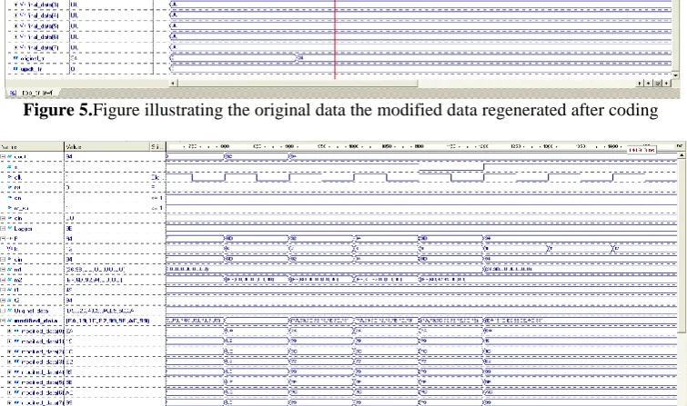
Figure 5.Figure illustrating the original data the modified data regenerated after coding
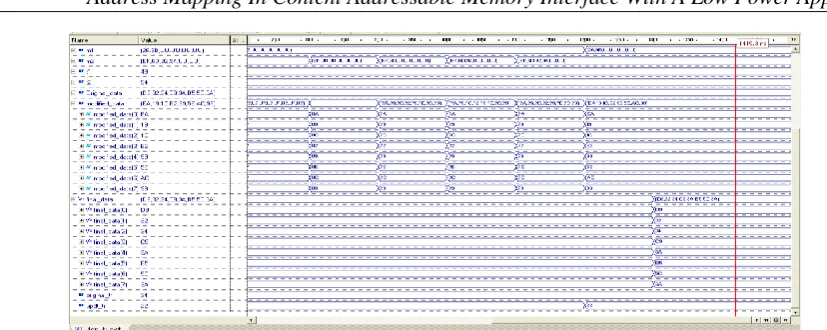
Figure 7. Illustrating the content of the memory buffered data for regeneration and the reconstructed data from it.
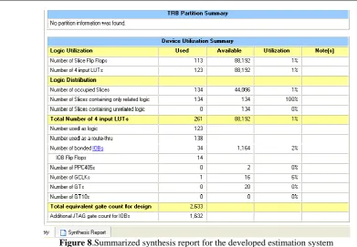
Implementation details on the targeted FPGA device, =============================================================== Final Results
Design Statistics
# IOs : 34
Cell Usage : # BELS : 542
# GND : 1
# INV : 5
# LUT1 : 124
# LUT2 : 66
# LUT3 : 15
# LUT4 : 38
# MUXCY : 147
# MUXF5 : 18
# MUXF6 : 2
# MUXF7 : 1
# VCC : 1
# XORCY : 124
# FlipFlops/Latches : 127
# FD : 15
# FDE : 80
# FDR : 32
# Clock Buffers : 1
# BUFGP : 1
# IO Buffers : 33
# IBUF : 17
# OBUF : 16
========================TIMING REPORT========================
Clock Information:
Speed Grade: -6
Minimum period: 7.693ns (Maximum Frequency: 129.984MHz) Minimum input arrival time before clock: 2.950ns
Figure 8.Summarized synthesis report for the developed estimation system
--- Release 9.1i - XPower SoftwareVersion:J.30
Copyright (c) 1995-2007 Xilinx, Inc. All rights reserved. Design: C:\Xilinx91i\Coding\transition.ncd
Preferences: transition.pcf Part: 2vpx70ff1704-6
Data version: PREVIEW,v1.0,05-28-03
Power summary: I(mA) P(mW) --- Total estimated power consumption: 112 ---
Vccint 1.50V: 85 112 Vccaux 2.50V: 20 50 Vcco25 2.50V: 2 4 ---
Clocks: 0 0 Inputs: 0 0 Logic: 0 0 Outputs:
Vcco25 0 0 Signals: 0 0 ---
Quiescent Vccint 1.50V: 85 112 Quiescent Vccaux 2.50V: 20 50 Quiescent Vcco25 2.50V: 2 4
Thermal summary:
--- Estimated junction temperature: 25C Ambient temp: 25C
Case temp: 25C Theta J-A: 0C/W
Figure 9. RTL view of the implemented system using Xilinx synthesizer.
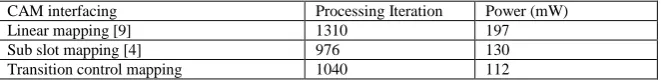
Figure 10: Comparative analysis of power dissipation in CAM operation
CAM interfacing Processing Iteration Power (mW)
Linear mapping [9] 1310 197
Sub slot mapping [4] 976 130
Transition control mapping 1040 112
Table 1: Result comparison of power dissipation in CAM operation
The observation of a CAM operation for a memory interfacing of 2KB, 16 bit memory interface tested over 4 different patterns is presented in table 1. The power utilization in the proposed transition controlling is observed to be 18mW lower than the conventional linear and sub slot approach.
V. Conclusion
This paper a new approach to addressing of content Addressable memory interfacing is developed. The proposes approach gives a significance of address pointer records and realignment of address register to minimize the correlative transition to optimize power consumption. In the proposed approach, the minimal cross correlation address logic are grouped to formulate the address logic. The power dissipation and the operational iteration are observed to be optimized, where an minimal increment in processing iteration is observed due to extra encoding and decoding operation, the power consumption is comparatively minimized due to reduced transition operation. This leads to a low power operation in CAM interfacing.
REFERENCES
[1]. D. Das, A. Roy, and H. Rahaman,„„ Design of content addressable memory architecture using carbon Nano tube field effect transistors,‟‟ in Progressing VLSI Design and Test, vol. 7373,
0 50 100 150 200 250
Pattern 1 Pattern 2 Pattern 3 Pattern 4
Linear
Sub slot
[2]. H. Rahaman, S. Chattopadhyay, and S. Chattopadhyay, Eds. Berlin, Germany: Springer-Verlag, 2012, pp. 233–242,ser. Lecture Notes in Computer Science.[Online]. Available: http://dx.doi.org/10.1007/978-3-642-31494-_27.
[3]. S. Kang et al., „„A 0.1-_m 1.8-V 256-MBphase-change random access memory(PRAM) with 66-MHz synchronous burst-read operation,‟‟ IEEE J. Solid-State Circuits, vol. 42, no. 1, pp. 210–218, Jan. 2007.
[4]. K. Degawa et al., „„A high-density ternary content-addressable memory using single-electron transistors,‟‟ in Proc. IEEE 36th Int. Symp. Multiple-Valued Logic,2006, DOI: 10.1109/ISMVL.2006.6.
[5]. M.-F. Chang et al., „„17.5 A 3T1R non volatile TCAM using MLC Re RAM with sub-1nssearch time,‟‟ in Proc. IEEE Int. Solid-State Circuits Conf., 2015, DOI: 10.1109/ISSCC.2015.7063054.
[6]. K. Nii et al., „„13.6 A 28 nm 400 MHz4-parallel 1.6 Gsearch/s 80MB ternary CAM,‟‟ in IEEE Int. IEEE Solid-State Circuits Conf. Dig. Tech. Papers, 2014, pp. 240–241.
[7]. S.Matsunaga et al., „„A 3.14 um 2 4T-2MTJ-cellfully parallel TCAM based on non volatile logic-in-memory architecture,‟‟ in Proc. IEEE Symp. VLSI Circuits, 2012, pp. 44–45.
[8]. J. Li, R. K. Montoye, M. Ishii, and L. Chang,„„1 MB 0.41_m22T-2R cell nonvolatile TCAM with two-bit encoding and clocked self-referenced sensing,‟‟ IEEE J. Solid-State Circuits, vol. 49, no. 4, pp. 896–907, Apr. 2014.
[9]. Y.-J. Hu, J.-F. Li, and Y.-J. Huang,„„3-D content addressable memory architectures,‟‟ in Proc. IEEE Int. Workshop Memory Technol. DesignTesting, 2009, pp. 59–64.
[10]. E. C. Oh and P. D. Franzon, „„Design considerations and benefits ofthree-dimensional ternary content addressable memory,‟‟ in Proc. IEEE Custom Integr. Circuits Conf., 2007,pp. 591–594.
[11]. D. Bhattacharya, A. Bhoj, and N. Jha, „„Design of efficient content addressable memories in high-performance FinFET technology,‟‟ IEEE Trans. Very LargeScale Integr. (VLSI) Syst., vol. 23, no. 5,pp. 963–967, May 2015.
[12]. A. McAuley and P. Francis, „„Fast routing table lookup using CAMs,‟‟ in Proc. IEEE12th Annu. Joint Conf. IEEE Comput. Commun. Soc., Netw.: Found. Future,1993, vol. 3, pp. 1382–1391.
[13]. F. Yu, R. Katz, and T. Lakshman, „„Gigabit rate packet pattern-matching using TCAM,‟‟ in Proc. 12th IEEE Int. Conf. Netw. Protocols, Oct. 2004,pp. 174–183.
[14]. K. Eshraghian, „„Memristormos content addressable memory (MCAM): Hybrid architecture for future high performance search engines,‟‟ IEEE Trans. Very Large Scale Integr. (VLSI) Syst., vol. 19, no. 8,pp. 1407–1417, Aug. 2011.
[15]. Q. Guo, X. Guo, Y. Bai, and E. Ipek, „„A resistive TCAM accelerator for data-intensive computing,‟‟ in Proc. 44thAnnu. IEEE/ACM Int. Symp. Microarchitect.,2011, pp. 339–350.
[16]. W. Webber, A. Moffat, and J. Zobel,„„A similarity measure for indefinite rankings,‟‟ ACM Trans. Inf. Syst.,vol. 28, no. 4, p. 20, 2010.
[17]. M. F. Porter, „„An algorithm for suffix stripping,‟‟ Program, Electron. LibraryInf. Syst., vol. 14, no. 3, pp. 130–137, 1980.
[18]. S. Narasimhan, M. Tabib-Azar, H. J. Chiel, and S. Bhunia, „„Neural data compression with wavelet transform: A vocabulary based approach,‟‟ in Proc. 3rd Int. IEEE/EMBS Conf. Neural Eng., 2007,pp. 666–669.
[19]. [82] S. Narasimhan, M. Cullins, H. J. Chiel, and S. Bhunia, „„Wavelet-based neural pattern analyzer for behaviorally significant burst pattern recognition,‟‟ in Proc. IEEE 30thAnnu. Int. Conf. Eng. Med. Biol. Soc., 2008,pp. 38–41.
[20]. [83] K. Pagiamtzis and A. Sheikholeslami, „„Content-addressable memory (CAM) circuits and architectures: A tutorial and survey,‟‟ IEEE J. Solid-State Circuits, vol. 41, no. 3,pp. 712–727, Mar. 2006.
[21]. M. Herlihy and J. E. B. Moss, “Transactional memory: Architectural support for lock-free data structures,‟‟ ACM SIGARCH Comput. Architect. News, vol. 21, no. 2, pp. 289–300,1993.
[22]. Z. Yan, H. Jiang, D. Feng, L. Tian, andY. Tan, „„SUV: A novel single-update version-management scheme for hardware transactional memory systems,‟‟ in Proc. IEEE 26th Int. Parallel Distrib. Process. Symp., May 2012,pp. 131–143.