Design of Improved Solar Energy Harvested
Hybrid Active Power Filter for Harmonic
Reduction, Power factor Correction and Current
Compensation
P. Karthika N. Shanthi
Assistant Professor Assistant Professor
Department of Electrical and Electronics Engineering Department of Electrical and Electronics Engineering Sri Sairam Institute of Technology Sri Sairam Institute of Technology
E. Maheswari Assistant Professor
Department of Electrical and Electronics Engineering Sri Sairam Institute of Technology
Abstract
This paper introduces the Hybrid Active Power Filter (HAPF) for power-factor correction, harmonic reduction and current compensation. The existing control scheme was implemented without load harmonic detection. In a hybrid active power filter(HAPF), the active part is used to filter out the higher order harmonics, while lower order harmonics are eliminated by passive filter tuned for 5th and 7th order harmonic frequencies. The compensation constraints are obtained by regulating the currents indirectly from the power mains. The reference currents of SAPF are generated by the dc-link voltage controller based on the active power balance of system. A high step-up converter, which is suitable for renewable energy system, is proposed in this paper to produce a dc-link voltage. Through a voltage multiplier module composed of switched capacitors and coupled inductors, a conventional interleaved boost converter obtains high step-up gain without operating at extreme duty ratio. Experimental results are shown for determining the effectiveness of the solar energy harvested HAPF-proposed control system.
Keywords: Hybrid active power filter, High step up converter, Harmonic compensation, Matlab/Simulink, Power factor correction
________________________________________________________________________________________________________
I.
I
NTRODUCTIONThe development of power electronic equipment, the intensive use of static converters, and the great number of domestic electronic-based applications have deteriorated the quality of the power mains system. These nonlinear loads generate current harmonics that can be asymmetric and can cause voltage drops on the supply network impedance resulting in unbalanced conditions. These effects can be worse in the case where the loads change randomly. Conventional solutions like passive filters alone for reducing the current harmonic pollution are ineffective. Moreover, standard regulations and recommendations regarding the power flow of electrical energy, such as IEC 61000-3-2 [1] and IEEE519 [2], have become restricted and this has stimulated the use of active power compensation. Active power compensation is normally achieved with the help of switching power converters connected to the network as an active filter. Combined use of active filter and passive filter helps to remove the higher and lower order harmonics. By providing high dc-link voltage from a Renewable energy source like solar by using a high step up converter it is possible to provide high compensation.
A suitable solution for compensating the power quality problems consists the use of current controller whose gains are adjusted by adaptation. The compensation requirements are obtained by regulating indirectly the currents of the power mains. In this case, the expected controlled grid currents must be sinusoidal, which addresses to control schemes like resonance-based techniques. In the proposed study, the amplitude of SAPF reference currents is generated by the dc-link voltage controller, based on the active power balance of system.
II.
S
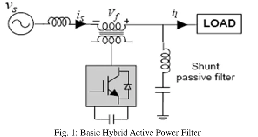
YSTEM DESCRIPTION AND MODELLINGFig. 1: Basic Hybrid Active Power Filter
The main advantage of the hybrid active power filter is that it requires a small rated converter compared to the similar pure active filter.
The active power filter can be divided into a power circuit and signal circuit. The power circuit produces the required current or voltage to be injected to the system. The main constituent of a power circuit is a Voltage Source Inverter (VSI) with a dc storage capacitor at dc bus. The VSI is made of power electronic switches such as IGBT, MOSFET’s etc. The required switching pulses for the VSI are provided by the signal circuit. The VSI is connected to the system through a coupling inductor or matching transformer or both.
Fig. 2: Hardware block diagram
The major parts of any active power filter set up are its control algorithm. The control algorithm calculates the instantaneous value of reference signal using the locally available current and voltage measurements. The algorithm used in active power filter should have a good steady state and transient response. The present work is focused to the control algorithms for single phase and three-phase shunt active power filter. In case of single phase active power filter, the control algorithm is required to generate a sinusoidal reference source current under both sinusoidal and distorted supply voltages. It should also ensure a good steady state and transient response. The three-phase active power filter algorithms make the source current balanced and sinusoidal.
The representation of an ideal active power filter or STATCOM consists of a voltage source which is supplying a non-linear load. The active power filter is represented by an ideal current source connected at the Point of Common Coupling (PCC), which injects the non-linear component of load current into the system. An ideal active power filter has infinite band width and it has no losses. This means, it can generate current of any shape with no losses in the system. Here the current source is replaced by a Voltage Source Inverter (VSI) supported by a dc link voltage produced by the high step up converter.
The operation of VSI is controlled by dsPIC microcontroller using input data such as PCC voltage, load current, filter current and dc capacitor voltage. The dsPIC computes the reference current of the active power filter using different control algorithms.
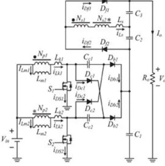
The proposed converter is a conventional interleaved boost converter integrated with a voltage multiplier module, and the voltage multiplier module is composed of switched capacitors and coupled inductors. The coupled inductors can be designed to extend step-up gain, and the switched capacitors offer extra voltage conversion ratio.
The advantages of the proposed converter are as follows.
lifetime of renewable energy sources and makes it suitable for high-power applications. 2) The converter achieves the high step-up gain that renewable energy systems require
3) Due to the lossless passive clamp performance, leakage energy is recycled to the output terminal. Hence, large voltage spikes across the main switches are alleviated, and the efficiency is improved.
4) Low cost and high efficiency are achieved by employment of the low-voltage-rated power switch with low RDS(ON); also, the voltage stresses on main switches and diodes are substantially lower than output voltage. 5) The inherent configuration of the proposed converter makes some diodes decrease conduction losses and alleviate
diode reverse recovery losses.
Fig. 3: Proposed high step up converter
III.
O
PERATING PRINCIPLE OF HIGH STEP UP CONVERTERThe proposed high step-up interleaved converter with a voltage multiplier module is shown in Fig. 2. The voltage multiplier module is composed of two coupled inductors and two switched capacitors and is inserted between a conventional interleaved boost converter to form a modified boost–flyback–forward interleaved structure. When the switches turn off by turn, the phase whose switch is in OFF state performs as a flyback converter, and the other phase whose switch is in ON state performs as a forward converter.
Primary windings of the coupled inductors with Np turns are employed to decrease input current ripple, and secondary windings of the coupled inductors with Ns turns are connected in series to extend voltage gain. The turn ratios of the coupled inductors are the same. The coupling references of the inductors are denoted by “·” and “∗”.
The equivalent circuit of the proposed converter is shown
in Fig. 3, where Lm1 and Lm2 are the magnetizing inductors; Lk1 and Lk2 represent the leakage inductors; Ls series leakage inductors in the secondary side; S1 and S2 denote the power switches. Cc1 and Cc2 are the switched capacitors; and C1, C2, and C3 are the output capacitors Dc1 and Dc2 are the clamp diodes
Fig. 4: Equivalent circuit of proposed model
Db1 and Db2 represent the output diodes for boost operation with switched capacitors, Df1 and Df2 represent the output diodes for
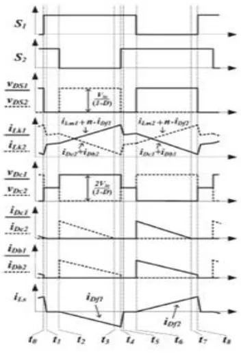
In the circuit analysis, the proposed converter operates in continuous conduction mode (CCM), and the duty cycles of the power switches during steady operation are greater than 0.5 and are interleaved with a 180◦ phase shift. The key steady waveform in one switching period of the proposed converter contains six modes.
Mode I [t0, t1]:
At t = t0, the power switch S2 remains in ON state, and the other power switch S1 begins to turn on. The diodes Dc1, Dc2, Db1, Db2,
and Df1 are reversed biased. The series leakage inductors Ls quickly release the stored energy to the output terminal via flyback–
forward diode Df2, and the current through series leakage inductors Ls decreases to zero. Thus, the magnetizing inductor Lm1 still
transfers energy to the secondary side of coupled inductors. The current through leakage inductor Lk1 increases linearly, and the
other current through leakage inductor Lk2 decreases linearly.
Mode II [t1, t2]:
At t = t1, Both of the power switches S1 and S2 remain in ON state, and all diodes are reversed biased. Both currents through leakage inductors Lk1 and Lk2 are increased linearly due to charging by input voltage source Vin.
Mode III [t2, t3]:
At t = t2, the power switch S1 remains in ON state, and the other power switch S2 begins to turn off.The diodes Dc1, Db1, and Df2 are
reversed biased. The energy stored in magnetizing inductor Lm2 transfers to the secondary side of coupled inductors, and the current
through series leakage inductors Ls flows to output capacitor C3 via flyback–forward diodeDf1. The voltage stress on power switch
S2 is clamped by clamp capacitor Cc1 which equals the output voltage of the boost converter. The input voltage source, magnetizing
inductor Lm2, leakage inductor Lk2,and clamp capacitor Cc2 release energy to the output terminal; thus, VC1 obtains a double output
voltage of the boost converter.
Fig. 5: Switching pattern
Mode IV [t3, t4]:
At t = t3, the current iDc2 has naturally decreased to zero due to the magnetizing current distribution, and hence, diode reverse
recovery losses are alleviated and conduction losses are decreased. Both power switches and all diodes remain in previous states except the clamp diode Dc2.
Mode V [t4, t5]:
At t = t4, the power switch S1 remains in ON state, and the other power switch S2 begins to turn on. The diodes Dc1, Dc2, Db1, Db2,
and Df2 are reversed biased. The series leakage inductors Ls quickly release the stored energy to the output terminal via flyback–
forward diode Df1, and the current through series leakage inductors decreases to zero. Thus, the magnetizing inductor Lm2 still
transfers energy to the secondary side of coupled inductors. The current through leakage inductor Lk2 increases linearly, and the
Mode VI [t5, t6]:
At t = t5, both of the power switches S1 and S2 remain in ON state, and all diodes are reversed biased. Both currents through leakage inductors Lk1 and Lk2 are increased linearly due to charging by input voltage source Vin.
Mode VII [t6, t7]:
At t = t6, the power switch S2 remains in ON state, and the other power switch S1 begins to turn off. The diodes Dc2, Db2, and Df1
are reversed biased. The energy stored in magnetizing inductor Lm1 transfers to the secondary side of coupled inductors, and the
current through series leakage inductors flows to output capacitor C2 via fly back–forward diode Df2. The voltage stress on power
switch S1 is clamped by clamp capacitor Cc2 which equals the output voltage of the boost converter. The input voltage source,
magnetizing inductor Lm1, leakage inductor Lk1, and clamp capacitor Cc1 release energy to the output terminal; thus, VC1 obtains
double output voltage of the boost converter.
Mode VIII [t7, t8]:
At t = t7, the current iDc1 has naturally decreased to zero due to the magnetizing current distribution, and hence, diode reverse
recovery losses are alleviated and conduction losses are decreased. Both power switches and all diodes remain in previous states except the clamp diode Dc1.
IV.
C
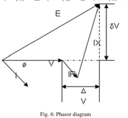
ALCULATION OF COMPENSATION CURRENTRole of Reactive Power on voltage and its regulation
E2=(V+ΔV)2+δv2
= (V+RICOSφ+XISINφ)2+ (XICOSφ-RISINφ)2
Hence, E2= [V+(RP/V)+(XQ/V)] 2+ [(XP/V)-(RQ/V)]2 ΔV= (RP+QX)/V
δV= (XP-RQ)/V δV<< (V+ΔV)
E2= [V+ (RP+QX)/V] 2 E-V= (RP+QX)/V=ΔV E-V= [XQ]/V
So the reactive power can be compensated either by improving the receiving voltage or by reducing the line reactance. Since the line reactance is fixed, it can be done only by increasing the voltage. Hence on injecting the current into the distribution we can improve the voltage and compensate the reactive power.
The voltage equation before nonlinear load is, Vt(t) = vm1 sin (t) The voltage and current equation after adding dc load is,
Vt(t)=
v
dc + vm1sin(t+φv1) + vm2sin(2t+φv2) + vm3sin(3t+φv3) + …+vmnsin(nt+φvn)Fig. 6: Phasor diagram
il(t)= idc +im1sin(t+φi1) +im2sin(2t+φi2) + im3sin(3t+φi3) +…imnsin(nt+φin) The source power can be calculated as,
Ps = [vm1imscosφs] / 2 With that the average power can be calculated as the product of vt(t) and il(t),
Ploss= kp x ev + ki evdt ; where, error voltage,ev = vref - vact The maximum value of source current can be calculated as,
ims = 2[Plavg+Ploss] / (vm1cosφs) The above equation can be reduced as,
is(t) = imssin(t-φs)
With the load current and the fundamental current, the injecting current can be found out as, ic*(t) = il(t) – is(t)
ic*(t) = il(t) – is(t)
V.
S
IMULATION CIRCUITVI.
S
IMULATION RESULTSFig. 7: Simulated voltage and current of uncompensated load
Fig. 8: FFT Analysis for Nonlinear load Fig. 9: Power factor before compensation
Fig. 11: FFT Analysis for compensated load Fig.12: Power factor before compensation
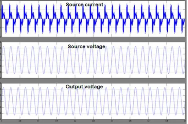
According to the simulation results the harmonic content has reduced to 13.66% in comparison to 99.05% without compensation.
VII.
H
ARDWAREThis is the experimental setup of Hybrid Active Power filter to filter out the harmonics and to compensate the source current.
Fig. 13: Hardware setup of hybrid active power filter
VIII.
S
COPE FOR FUTURE WORKThe Hybrid active power filter is a major scope of application for the future power system,i.e For sustainable growth in power system, it is needed to utilize the renewable energy resources like wind, biomass, hydel power, co-generation, etc. The integration of wind energy into existing power system generates power quality issues such as voltage transients, instability, etc. Adaptive shunt hybrid filters are suggested for improving power quality issues, when generation rapidly changes with wind speed. This can also be implemented with other control schemes such as high efficient fuzzy logic technique to improve the efficiency
IX.
C
ONCLUSIONThe details of Renewable energy harvested Hybrid Active Power Filter are presented. Based on the design details illustrated, a prototype is developed in the laboratory. The experimental results demonstrate the compensator effectively compensates harmonic components of the load current and consequently utility currents are balanced and sinusoidal with unity phase relationship with their voltages in respective phases. Also, the method can work irrespective of supply voltage quality, whether it is sinusoidal or distorted. It is observed that the experimental results are consistent with the simulation results.
R
EFERENCES[1] Ajjarappu, V., Lee, B., “Bibliography on voltage stability,” IEEE Transactions on Power Systems, Vol. 12, No. 1, February 1997.
[2] Kundur, P., Paserba, J., Ajjarappu, V., et.al, “Definition and classification of power System stability IEEE/CIGRE joint task force on stability terms and definitions,” IEEE Transactions on Power Systems, Vol. 19, No. 3, pp. 1387-1401, August 2004.
[3] Kundur, P., Power System Stability and Control, New York: McGraw-Hill, 1994. [4] Taylor, C.W., Power System Voltage Stability, New York: McGraw-Hill, 1994.
[5] Van Cutsem, T., “Voltage instability: Phenomenon, counter measures and analysis Methods,” IEEE Proceedings, Vol. 88, pp. 208-227, 2000.
[6] Ca˜nizares, C.A., “Voltage Stability Assessment: Concepts Practices and Tools,” IEEE PES Power System Stability Subcommittee Special Publication, SP101PSS, Technical Report, 2002.
[7] Mansour, Y., Xu, W., Alverado, F., Rinzin, C., “SVC Placement Using Critical Modes of Voltage Instability,” IEEE Transactions on Power Systems, Vol. 9, No. 2, pp. 757-763, May 1994.
[8] Lagonotte, P., Sabonnadiere, J.C., Leost, J.Y., Paul, J.P., “Structural analysis of the Electrical system: application to the secondary voltage control in France,” IEEE Transactions on Power Systems, Vol. 2,
Pp.479- 484, 1989.